

Page 1

6121 Baker Road,
Suite 108
Minnetonka, MN 55345
www.chtechnology.com
Phone (952) 933-6190
Fax (952) 933-6223
1-800-274-4284
Thank you for downloading this document from C&H Technology, Inc.
Please contact the C&H Technology team for the following questions -
Technical
Application
Assembly
Availability
Pricing
Phone – 1-800-274-4284
E-Mail – sales@chtechnology.com
www.chtechnology.com - SPECIALISTS IN POWER ELECTRONIC COMPONENTS AND ASSEMBLIES - www.chtechnology.com
Page 2
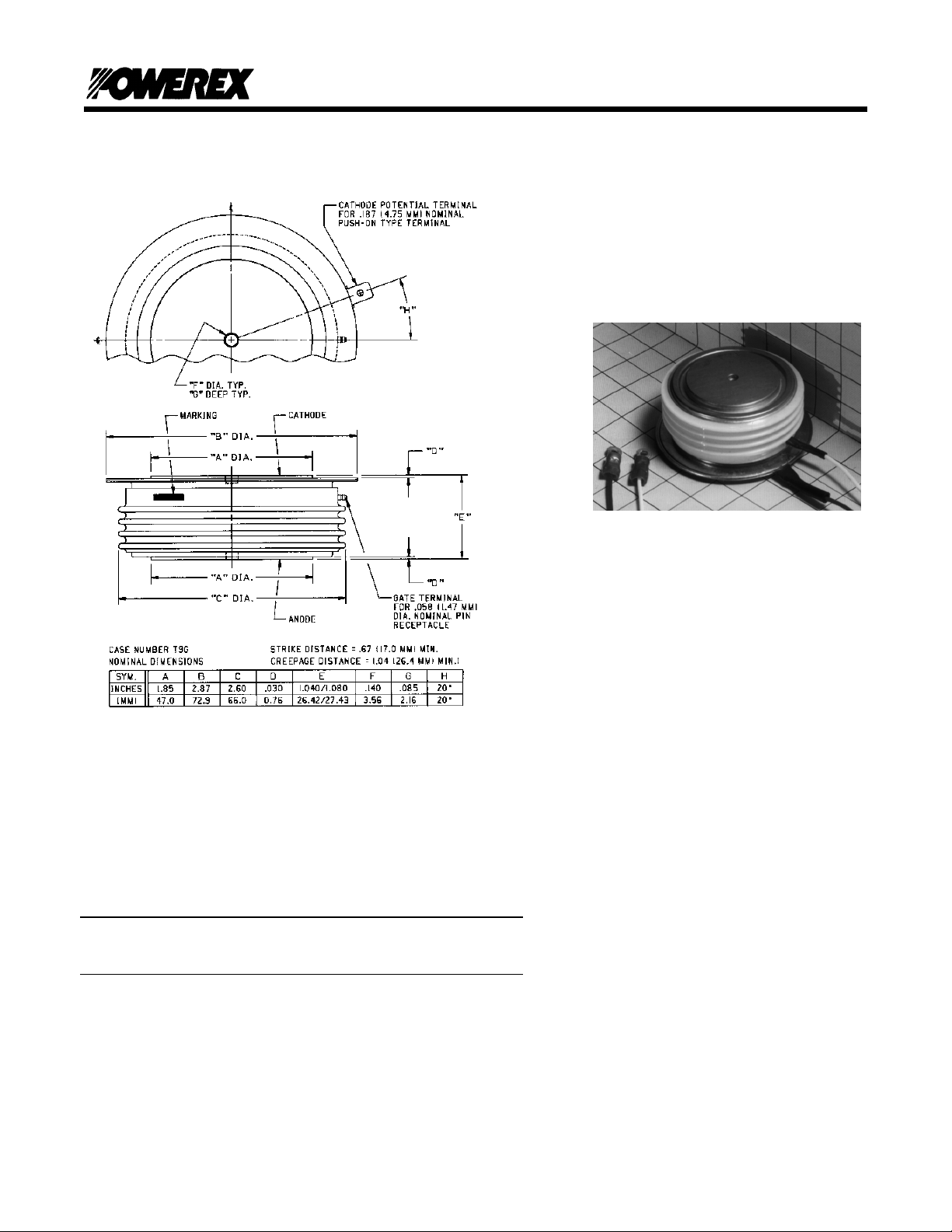
T9G0
1660A
Powerex, Inc., 200 Hillis Street, Youngwood, Pennsylvania 15697-1800 (724)925-7272 Phase Control Thyristor
1660 Amperes/Up to 1800 Volts
Description:
The T9GO is a medium voltage, hi gh current disc
pack SCR employing a cent er fired, amplifying
gate structure suitabl e for operation to 400 Hz.
The amplifying gate allows this SCR to be
reliably operated at high di/dt and high dv/ dt
conditions in phase control appl i cations.
Ordering Information
Select the compl ete 10 digit device part number f rom the table below,
ie. T9G0161603 is a 1600V 1660A Phase Control S CR.
T9G0
Voltage
V
DRM
V
RRM
1200V
1400V
1600V
1800V
Voltage
Code
12
14
16
18
Current
IT
(avg)
1660
A
Current
Code
16 0 3
Tq
Features:
Low On-State Voltage
High di/dt Capability
High dv/dt Capability
Hermetic Packagi ng
Excellent Surge and I
Replaces PRX C450 Thyristor
2
t Ratings
Applications:
DC Power Supplies
Motor Controls
AC Switches
I
GT
022300
Page 3

5
-
y
r
T9G0
1660A
Powerex, Inc., 200 Hillis Street, Youngwood, Pennsylvania 15697-1800 (724)92
7272 Phase Control Th
risto
1660 Amperes/Up to 1800 Volts
Absolute Maximum Ratings
Characteristics
Repetitive Peak Reverse Voltage V
Repetitive Peak Forward Voltage V
RMS On-State Current, T
Average Current 180°°°° Sine Wave, TC=70°°°°C
RMS On-State Current, T
Average Current 180°°°° Sine Wave, TC=55°°°°C
Peak One Cycle Surge On-State Current (Non-Repetitive) 60Hz, VR = 0V I
=70°°°°C
C
=55°°°°C
C
Symbol
1200 1400 1600 1800 V
RRM
1200 1400 1600 1800 V
DRM
I
I
I
I
2600 A
T(RMS)
1660 A
T(AV)
3140 A
T(RMS)
2000 A
T(AV)
29,000 A
TSM
Units
Peak One Cycle Surge On-State Current (Non-Repetitive) 50Hz, VR = 0V I
Critical Rate-of-Rise of On-State Current (Non-Repetitive)* di/dt 1000
Critical Rate-of-Rise of On-State Current (Repetitive)* di/dt 400
I2t for Fusing for One Cycle, 60 Hz I2t 3.54 x 10⁶ A
I2t for Fusing for One Cycle, 50 Hz I2t 3.75 x 10⁶ A
27,400 A
TSM
A/µµµµs
A/µµµµs
2
s
2
s
Peak Gate Power Dissipation PGM 2000 W
Average Gate Power Dissipation P
Operating Temperature TJ
Storage Temperature T
Approximate Weight 1
Mounting Force 5500 – 6000
*
NON-JEDEC Test Conditions
5 W
G(av)
-40 to 125°°°°C °°°°C
STG
-40 to 150°°°°C °°°°C
lb.
0.45
Kg
lb.
2450 -- 2670
Kg
022300
Page 4

A
T9G0
1660
Powerex, Inc., 200 Hillis Street, Youngwood, Pennsylvania 15697-1800 (724)925-7272
Phase Control Thyristor
1660 Amperes/Up to 1800 Volts
Electrical Characteristics, T
=25°°°°C unless otherwise specified
J
Characteristics Symbol Test Conditions Min. Typ. Max. Units
Repetitive Peak Reverse Leakage
I
RRM
=125°°°°C, V
T
J
R=VRRM
75 mA
Current
Repetitive Peak Forward Leakage
I
DRM
=125°°°°C, V
T
J
D=VDRM
75 mA
Current
Peak On-State Voltage VTM I
=1500A
TM
1.25 V
Duty Cycle < 0.01%
Threshold Voltage, Low-level
Slope Resistance, Low-level
V
TM
= V
TO + rT
x ITM
Threshold Voltage, High-level
Slope Resistance, High-level
VTM = V
VTM Coefficients T
TO + rT
x I
TM
J
=125°°°°C, I = 15% I
B= .136
VTM = A + B x ln(I
) + C x I
TM
TM
+ D x (I
V
(TO)1
r
T1
V
(TO)2
r
T2
to I
AV
TSM
½
)
C= 1.35-4
TM
=125°°°°C, I = 15% IAV to ππππI
T
J
=125°°°°C, I = ππππI
T
J
to I
AV
TSM
AV
.834
.164
.993
.126
A= .109
D= -.00457
Typical Delay Time td
VD = VDRM
1
Gate Drive: 20V - 20Ω – 0.1µs
V
mΩΩΩΩ
V
mΩΩΩΩ
µµµµs
Typical Turn-Off Time tq
=125°°°°C, I
T
J
=400A, VR>50V,
T
150
µµµµs
reapplied dv/dt=20V/µµµµs linear to 80%
V
DRM
Minimum Critical dv/dt linear to V
DRM
dv/dt
Gate Trigger Current IGT
Gate Trigger Voltage VGT
Peak Reverse Gate Voltage V
GRM
=125°°°°C, V
T
J
=80% rated
DRM
Gate Open
=25°°°°C, V
T
J
=25°°°°C, V
T
J
=12V
D
=12V
D
5 V
400
V/µµµµs
30 100 200 mA
0.8 1.5 3.0 V
Thermal Characteristics
Characteristics Symbol Min. Typ. Max. Units
Maximum Thermal Resistance, Double
Sided Cooling
Junction to Case
Case to Sink
R
ΘΘΘΘJC
R
ΘΘΘΘCS
.023
.006
°°°°C/W
°°°°C/W
022300
Page 5

(
)
_
A
Powerex, Inc., 200 Hillis Street, Youngwood, Pennsylvania 15697-1800 (724)925-7272
T9G0
1660
Phase Control Thyristor
Maximum On-State Forward Voltage Drop
(Tj = 125°C)
7
6
5
4
3
2
1
On-State Voltage -- VTM -- Volts
0
100 1000 10000 100000
Instantaneous Current -- ITM -- Amperes
Maximum Allowable Case Temperature
(Sinusoidal Waveform)
130
120
110
Maximum Transient Thermal Impedance
0.025
0.02
0.015
0.01
°C/Watt
0.005
Thermal Impedance -- ZΘjc --
0
0.001 0.01 0.1 1 10 100
Junction to Case
Time -- t -- Seconds
Maximum Allowable Case Temperature
(Sinusoidal Waveform)
130
120
110
100
90
80
70
Max. Case Temperature - Tcase -°C
60
0 500 1000 1500 2000
Average On-State Current - If(av) - Amperes
3000
2500
2000
1500
1000
500
Max. Power Dissipation Per Diode - Watts_
0
0 500 1000 1500 2000
15°
30°
60°
90°
120°
Maximum On-State Power Dissipation
(Sinusoidal Waveform)
120°
90°
60°
15°
Average On-State Current - If(av) - Amperes
30°
180°
180°
100
90
80
70
Max. Case Temperature - Tcase -°C_
60
0 500 1000 1500 2000
15°
30°
60°
90°
120°
180°
Average On-State Current - If(av) - Amperes
Maximum On-State Power Dissipation
(Rectangular Waveform)
4000
3500
3000
2500
2000
1500
1000
500
Max. Power Dissipation Per Diode - Watt s_
0
0 500 1000 1500 2000 2500 3000
30°
15°
90°
60°
180°
120°
Average On-State Current - If(av) - Amperes
360°
270°
022300
 Loading...