


6121 Baker Road,
Suite 108
Minnetonka, MN 55345
www.chtechnology.com
Phone (952) 933-6190
Fax (952) 933-6223
1-800-274-4284
Thank you for downloading this document from C&H Technology, Inc.
Please contact the C&H Technology team for the following questions -
Technical
Application
Assembly
Availability
Pricing
Phone – 1-800-274-4284
E-Mail – sales@chtechnology.com
www.chtechnology.com - SPECIALISTS IN POWER ELECTRONIC COMPONENTS AND ASSEMBLIES - www.chtechnology.com
ST730CLPbF Series
Vishay High Power Products
Phase Control Thyristors
(Hockey PUK Version), 990 A
FEATURES
• Center amplifying gate
• Metal case with ceramic insulator
• International standard case TO-200AC (B-PUK)
• Lead (Pb)-free
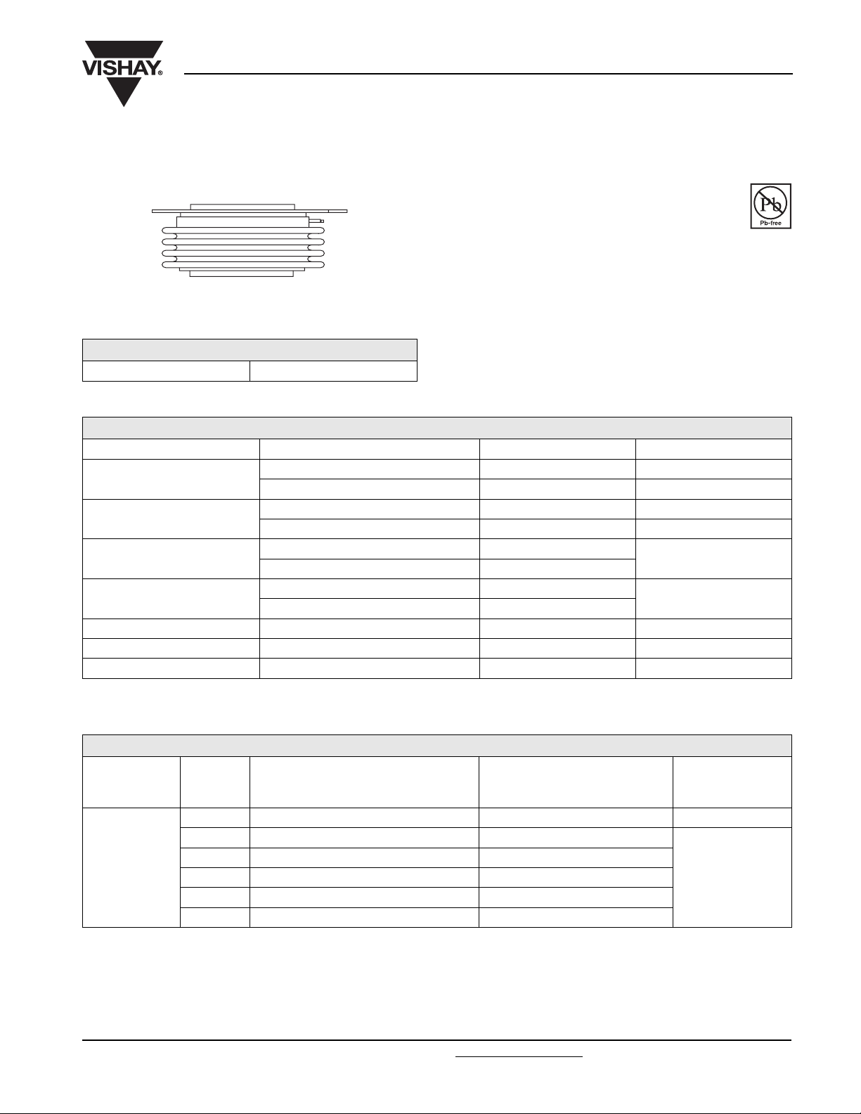
TO-200AC (B-PUK)
PRODUCT SUMMARY
I
T(AV)
990 A
MAJOR RATINGS AND CHARACTERISTICS
PARAMETER TEST CONDITIONS VALUES UNITS
I
T(AV)
I
T(RMS)
I
TSM
2
I
t
V
DRM/VRRM
t
q
T
J
T
hs
T
hs
50 Hz 17 800
60 Hz 18 700
50 Hz 1591
60 Hz 1452
Typical 150 µs
• Designed and qualified for industrial level
TYPICAL APPLICATIONS
• DC motor controls
• Controlled DC power supplies
• AC controllers
990 A
55 °C
2000 A
25 °C
A
kA2s
800 to 2000 V
- 40 to 125 °C
RoHS
COMPLIANT
ELECTRICAL SPECIFICATIONS
VOLTAGE RATINGS
V
TYPE NUMBER
ST730C..L
Document Number: 94414 For technical questions, contact: ind-modules@vishay.com
Revision: 06-May-08 1
VOLTAGE
CODE
08 800 900
12 1200 1300
14 1400 1500
16 1600 1700
18 1800 1900
20 2000 2100
DRM/VRRM
, MAXIMUM REPETITIVE PEAK
AND OFF-STATE VOLTAGE
V
V
, MAXIMUM
NON-REPETITIVE PEAK VOLTAGE
RSM
V
I
DRM/IRRM
AT T
= TJ MAXIMUM
J
www.vishay.com
MAXIMUM
mA
80
ST730CLPbF Series
Vishay High Power Products
Phase Control Thyristors
(Hockey PUK Version), 990 A
ON-STATE CONDUCTION
PARAMETER SYMBOL TEST CONDITIONS VALUES UNITS
Maximum average on-state current
at heatsink temperature
Maximum RMS on-state current I
I
T(RMS)
Maximum peak, one-cycle
non-repetitive surge current
2
Maximum I
Maximum I
t for fusing I2t
2
√t for fusing I2√t t = 0.1 to 10 ms, no voltage reapplied 15 910 kA2√s
Low level value of threshold voltage V
High level value of threshold voltage V
Low level value of on-state slope resistance r
High level value of on-state slope resistance r
Maximum on-state voltage V
Maximum holding current I
Typical latching current I
T(AV)
180° conduction, half sine wave
double side (single side) cooled
DC at 25 °C heatsink temperature double side cooled 2000
I
TSM
T(TO)1
T(TO)2
t1
t2
TM
H
L
t = 10 ms
t = 8.3 ms 18 700
t = 10 ms
t = 8.3 ms 15 700
t = 10 ms
t = 8.3 ms 1452
t = 10 ms
t = 8.3 ms 1027
(16.7 % x π x I
(I > π x I
(16.7 % x π x I
(I > π x I
Ipk = 2000 A, TJ = TJ maximum, tp = 10 ms sine pulse 1.62 V
TJ = 25 °C, anode supply 12 V resistive load
No voltage
reapplied
100 % V
reapplied
No voltage
RRM
Sinusoidal half wave,
initial T
= TJ maximum
J
reapplied
100 % V
RRM
reapplied
< I < π x I
T(AV)
), TJ = TJ maximum 1.12
T(AV)
< I < π x I
T(AV)
), TJ = TJ maximum 0.27
T(AV)
), TJ = TJ maximum 0.98
T(AV)
), TJ = TJ maximum 0.32
T(AV)
990 (375) A
55 (85) °C
17 800
15 000
1591
1125
600
1000
A
kA2s
V
mΩ
mA
SWITCHING
PARAMETER SYMBOL TEST CONDITIONS VALUES UNITS
Maximum non-repetitive rate of rise
of turned-on current
Typical delay time t
Typical turn-off time t
dI/dt
d
q
Gate drive 20 V, 20 Ω, t
T
= TJ maximum, anode voltage ≤ 80 % V
J
≤ 1 µs
r
DRM
Gate current 1 A, dIg/dt = 1 A/µs
V
= 0.67 % V
d
, TJ = 25 °C
DRM
ITM = 750 A, TJ = TJ maximum, dI/dt = 60 A/µs,
V
= 50 V, dV/dt = 20 V/µs, gate 0 V 100 Ω, tp = 500 µs
R
1000 A/µs
1.0
µs
150
BLOCKING
PARAMETER SYMBOL TEST CONDITIONS VALUES UNITS
Maximum critical rate of rise of
off-state voltage
Maximum peak reverse and
off-state leakage current
dV/dt T
I
RRM,
I
DRM
= TJ maximum linear to 80 % rated V
J
TJ = TJ maximum, rated V
DRM/VRRM
DRM
500 V/µs
applied 80 mA
www.vishay.com For technical questions, contact: ind-modules@vishay.com
Document Number: 94414
2 Revision: 06-May-08

ST730CLPbF Series
Phase Control Thyristors
Vishay High Power Products
(Hockey PUK Version), 990 A
TRIGGERING
PARAMETER SYMBOL TEST CONDITIONS
Maximum peak gate power P
Maximum average gate power P
Maximum peak positive gate current I
Maximum peak positive gate voltage + V
Maximum peak negative gate voltage - V
GM
G(AV)
GM
TJ = TJ maximum, tp ≤ 5 ms 10.0
TJ = TJ maximum, f = 50 Hz, d% = 50 2.0
TJ = TJ maximum, tp ≤ 5 ms 3.0 A
GM
TJ = TJ maximum, tp ≤ 5 ms
GM
TJ = - 40 °C
DC gate current required to trigger I
DC gate voltage required to trigger V
DC gate current not to trigger I
DC gate voltage not to trigger V
GT
GT
GD
GD
= 25 °C 100 200
J
T
= 125 °C 50 -
J
TJ = - 40 °C 2.5 -
= 25 °C 1.8 3.0
T
J
T
= 125 °C 1.1 -
J
Maximum required gate trigger/
current/voltage are the lowest
value which will trigger all units
12 V anode to cathode applied
Maximum gate current/voltage
not to trigger is the maximum
TJ = TJ maximum
value which will not trigger any
unit with rated V
anode to
DRM
cathode applied
VALUES
TYP. MAX.
20
5.0
200 -
10 mA
0.25 V
UNITS
W
V
mAT
V
THERMAL AND MECHANICAL SPECIFICATIONS
PARAMETER SYMBOL TEST CONDITIONS VALUES UNITS
Maximum operating junction temperature range T
Maximum storage temperature range T
Maximum thermal resistance, junction to heatsink R
Maximum thermal resistance, case to heatsink R
J
Stg
thJ-hs
thC-hs
DC operation single side cooled 0.073
DC operation double side cooled 0.031
DC operation single side cooled 0.011
DC operation double side cooled 0.006
Mounting force, ± 10 %
Approximate weight 255 g
Case style See dimensions - link at the end of datasheet TO-200AC (B-PUK)
ΔR
CONDUCTION ANGLE
CONDUCTION
thJ-hs
180°
120°
90°
60°
30°
SINUSOIDAL CONDUCTION RECTANGULAR CONDUCTION
SINGLE SIDE DOUBLE SIDE SINGLE SIDE DOUBLE SIDE
0.009 0.009 0.006 0.006
0.011 0.011 0.010 0.011
0.014 0.014 0.015 0.015
0.020 0.020 0.021 0.021
0.036 0.036 0.036 0.036
TEST CONDITIONS UNITS
T
= TJ maximum K/W
J
Note
• The table above shows the increment of thermal resistance R
when devices operate at different conduction angles than DC
thJ-hs
- 40 to 125
- 40 to 150
14 700
(1500)
°C
K/W
N
(kg)
Document Number: 94414 For technical questions, contact: ind-modules@vishay.com
www.vishay.com
Revision: 06-May-08 3

ST730CLPbF Series
Vishay High Power Products
130
120
110
100
90
80
70
60
50
40
0 100200300400500600700
Maximum Allowable Heatsink Temperature (°C)
Average On-state Current (A)
Fig. 1 - Current Ratings Characteristics
130
120
110
100
90
80
70
60
50
40
30
20
020040060080010001200
Maximum Allowable Heatsink Temperature (°C)
Averag e On-state Current (A)
Fig. 2 - Current Ratings Characteristics
ST7 3 0 C . . L Se r i e s
(Single Side Cooled)
R (DC) = 0.073 K/ W
thJ-hs
Cond uction Angle
30°
60°
90°
ST730C . .L Se ries
(Single Side Cooled)
R (DC) = 0.073 K/ W
thJ-hs
Cond uc tion Period
30°
60°
90°
120°
180°
120°
DC
Phase Control Thyristors
(Hockey PUK Version), 990 A
130
120
110
100
90
80
70
60
50
180°
40
30
20
0 400 800 1200 1600 2000 2400
Maximum Allowable Heatsink Temperature (°C)
Fig. 4 - Current Ratings Characteristics
2500
2000
1500
1000
500
0
Maximum Average On-state Power Loss (W)
0 200 400 600 800 1000 1200 1400
Fig. 5 - On-State Power Loss Characteristics
ST7 30 C . . L Se r i e s
(Double Side Cooled)
R (DC) = 0.031 K/ W
thJ-hs
Conduction Period
30°
60°
90°
120°
180°
DC
Av e ra ge On-sta t e C urre n t (A)
180°
120°
90°
60°
30°
Average On-stat e Current (A)
RM S Li m i t
Cond uction Angle
ST730C ..L Se ries
T = 125°C
J
130
120
110
100
90
80
70
60
50
40
30
20
0 200 400 600 800 1000 1200 1400
Maximum Allowable Heatsink Temperature (°C)
ST7 30 C . . L Se r i e s
(Double Side Cooled)
R (DC) = 0.031 K/W
thJ-hs
Cond uction Ang le
30°
60°
90°
120°
Fig. 3 - Current Ratings Characteristics
180°
3500
3000
2500
2000
1500
1000
500
Maximum Average On-state Power Loss (W)
DC
180°
120°
90°
60°
30°
RM S Li m i t
Conduction Period
ST730C ..L Se rie s
T = 1 25 ° C
J
0
0 400 800 1200 1600 2000 2400
Average O n-state Curren t ( A)
Fig. 6 - On-State Power Loss Characteristics
www.vishay.com For technical questions, contact: ind-modules@vishay.com
Document Number: 94414
4 Revision: 06-May-08

ST730CLPbF Series
Phase Control Thyristors
(Hockey PUK Version), 990 A
16000
At Any Ra ted Load Condition And With
Rated V Applied Following Surge.
15000
14000
13000
12000
11000
10000
9000
ST7 3 0 C . . L Se r i e s
8000
Pe a k Half Sine Wave On -sta te Current (A)
7000
110100
Numb er Of Equal Amplitude Half Cyc le Current Pulses (N)
Fig. 7 - Maximum Non-Repetitive Surge Current
RRM
Init ia l T = 125°C
J
@ 60 Hz 0.0083 s
@ 50 Hz 0.0100 s
Single and Double Side Cooled
10000
T = 2 5 ° C
J
18000
17000
16000
15000
14000
13000
12000
11000
10000
9000
8000
Peak Half Sine Wa ve On-state Current (A)
7000
T = 125°C
J
Vishay High Power Products
Maximum Non Repetitive Surge Current
Ve rsus Pulse Tra in Du ra t ion . Contro l
Of Conduc tion May Not Be Mainta ined .
ST7 30 C . . L Se r i e s
0.01 0.1 1
Pulse Train Duration (s)
Fig. 8 - Maximum Non-Repetitive Surge Current
Single and Double Side Cooled
Init ial T = 125°C
No Voltage Reapplied
Ra t e d V Re a p p l ie d
J
RRM
1000
ST7 3 0 C . . L Se r i e s
Instantaneous On-state Current (A)
100
0.5 1 1.5 2 2.5 3 3.5
Instantaneous On-state Voltage (V)
Fig. 9 - On-State Voltage Drop Characteristics
0.1
Steady State Value
R = 0.073 K/ W
thJ-hs
thJ-hs
0.001
Transient Thermal Impedance Z (K/W)
(Single Side Cooled)
R = 0.031 K/ W
thJ-hs
(Double Side Cooled)
(DC Operation)
0.01
ST7 30 C . . L Se r i e s
0.001 0.01 0.1 1 10
Sq u a r e W a v e Pu l se D u r a t i o n ( s)
Fig. 10 - Thermal Impedance Z
Characteristics
thJ-hs
Document Number: 94414 For technical questions, contact: ind-modules@vishay.com
www.vishay.com
Revision: 06-May-08 5

DIMENSIONS in millimeters (inches)
Outline Dimensions
Vishay High Power Products
TO-200AC (B-PUK)
Case Style TO-200AC (B-PUK)
Creepage distance: 36.33 (1.430) minimum
Strike distance: 17.43 (0.686) minimum
0.7 (0.03) MIN.
27 (1.06) MAX.
0.7 (0.03) MIN.
34 (1.34) DIA. MAX.
2 places
53 (2.09) DIA. MAX.
58.5 (2.3) DIA. MAX.
6.2 (0.24) MIN.
Pin receptacle
AMP. 60598-1
4.7 (0.18)
20° ± 5°
36.5 (1.44)
2 holes DIA. 3.5 (0.14) x 2.5 (0.1) deep
Quote between upper and lower pole pieces has to be considered after
application of mounting force (see thermal and mechanical specification)
Document Number: 95076 For technical questions concerning discrete products, contact: diodes-tech@vishay.com
Revision: 01-Aug-07 For technical questions concerning module products, contact: ind-modules@vishay.com
www.vishay.com
1

ST730CLPbF Series
Vishay High Power Products
100
Rectangular gate pulse
a) Recommended load line for
rated di/dt : 20V, 10ohms; tr<=1 µs
b) Recommended load line for
<=30% rated di/ dt : 10V, 10oh m s
10
tr<=1 µs
1
In st a nt a n e o us G a t e V o lt a g e ( V )
0.1
0.001 0.01 0.1 1 10 100
ORDERING INFORMATION TABLE
VGD
IGD
Phase Control Thyristors
(Hockey PUK Version), 990 A
(1) PGM = 10W, tp = 4ms
(2) PGM = 20W, tp = 2ms
(3) PGM = 40W, tp = 1ms
(4) PGM = 60W, tp = 0.66ms
(a)
(b)
Tj = - 40 °C
Tj = 2 5 ° C
Tj = 1 25 ° C
Device: ST730C..L Series
Instantaneous Gate Current (A)
Fig. 11 - Gate Characteristics
Fre q ue n c y Lim it e d b y PG ( AV )
(1)
(2)
(3)
(4)
Device code
ST 73 0 C 20 L 1 - PbF
324
51
6789
1 - Thyristor
2 - Essential part number
3 - 0 = Converter grade
4
- C = Ceramic PUK
5
- Voltage code x 100 = V
6
- L = PUK case TO-200AC (B-PUK)
7
- 0 = Eyelet terminals (gate and auxiliary cathode unsoldered leads)
(see Voltage Ratings table)
RRM
1 = Fast-on terminals (gate and auxiliary cathode unsoldered leads)
2 = Eyelet terminals (gate and auxiliary cathode soldered leads)
3 = Fast-on terminals (gate and auxiliary cathode soldered leads)
8 - Critical dV/dt:
None = 500 V/µs (standard selection)
L = 1000 V/µs (special selection)
9 - Lead (Pb)-free
LINKS TO RELATED DOCUMENTS
Dimensions http://www.vishay.com/doc?95076
www.vishay.com For technical questions, contact: ind-modules@vishay.com
6 Revision: 06-May-08
Document Number: 94414
 Loading...