

Page 1

6121 Baker Road,
Suite 108
Minnetonka, MN 55345
www.chtechnology.com
Phone (952) 933-6190
Fax (952) 933-6223
1-800-274-4284
Thank you for downloading this document from C&H Technology, Inc.
Please contact the C&H Technology team for the following questions -
Technical
Application
Assembly
Availability
Pricing
Phone – 1-800-274-4284
E-Mail – sales@chtechnology.com
www.chtechnology.com - SPECIALISTS IN POWER ELECTRONIC COMPONENTS AND ASSEMBLIES - www.chtechnology.com
Page 2
Vishay High Power Products
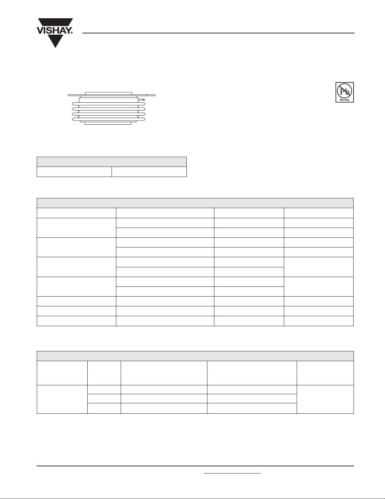
Phase Control Thyristors
(Hockey PUK Version), 790 A
FEATURES
• Center amplifying gate
ST650C..L Series
• Metal case with ceramic insulator
• International standard case TO-200AC (B-PUK)
• Lead (Pb)-free
TO-200AC (B-PUK)
TYPICAL APPLICATIONS
PRODUCT SUMMARY
I
T(AV)
790 A
• DC motor control
• Controlled DC power supplies
• AC controllers
MAJOR RATINGS AND CHARACTERISTICS
PARAMETER TEST CONDITIONS VALUES UNITS
I
T(AV)
I
T(RMS)
I
TSM
2
I
t
V
DRM/VRRM
t
q
T
J
T
hs
T
hs
50 Hz 10 100
60 Hz 10 700
50 Hz 510
60 Hz 475
Typical 200 µs
790 A
55 °C
1557 A
25 °C
A
kA2s
2000 to 2400 V
- 40 to 125 °C
RoHS
COMPLIANT
ELECTRICAL SPECIFICATIONS
VOLTAGE RATINGS
V
TYPE NUMBER
ST650C..L
Document Number: 93738 For technical questions, contact: ind-modules@vishay.com
Revision: 15-May-08 1
VOLTAGE
CODE
20 2000 2100
22 2200 2300
24 2400 2500
DRM/VRRM
PEAK AND OFF-STATE VOLTAGE
, MAXIMUM REPETITIVE
V
V
, MAXIMUM
NON-REPETITIVE PEAK VOLTAGE
RSM
V
I
DRM/IRRM
= TJ MAXIMUM
AT T
J
www.vishay.com
MAXIMUM
mA
80
Page 3
ST650C..L Series
Vishay High Power Products
Phase Control Thyristors
(Hockey PUK Version),
790 A
ON-STATE CONDUCTION
PARAMETER SYMBOL TEST CONDITIONS VALUES UNITS
Maximum average on-state current
at heatsink temperature
Maximum RMS on-state current I
I
T(RMS)
Maximum peak, one-cycle
non-repetitive surge current
Maximum I
Maximum I
2
t for fusing I2t
2
√t for fusing I2√t t = 0.1 to 10 ms, no voltage reapplied 5100 kA2√s
Low level value of threshold voltage V
High level value of threshold voltage V
Low level value of on-state slope resistance r
High level value of on-state
slope resistance
Maximum on-state voltage V
Maximum holding current I
Typical latching current I
T(AV)
180° conduction, half sine wave
Double side (single side) cooled
DC at 25 °C heatsink temperature double side cooled 1857
I
TSM
T(TO)1
T(TO)2
t1
r
t2
TM
H
L
t = 10 ms
t = 8.3 ms 10 700
t = 10 ms
t = 8.3 ms 9150
t = 10 ms
t = 8.3 ms 475
t = 10 ms
t = 8.3 ms 347
(16.7 % x π x I
(I > π x I
(16.7 % x π x I
(I > π x I
Ipk = 1700 A, TJ = TJ maximum, tp = 10 ms sine pulse 2.07 V
TJ = 25 °C, anode supply 12 V resistive load
No voltage
reapplied
100 % V
RRM
reapplied
No voltage
Sinusoidal half wave,
initial T
= TJ maximum
J
reapplied
100 % V
RRM
reapplied
< I < π x I
T(AV)
), TJ = TJ maximum 1.13
T(AV)
< I < π x I
T(AV)
), TJ = TJ maximum 0.35
T(AV)
), TJ = TJ maximum 1.04
T(AV)
), TJ = TJ maximum 0.61
T(AV)
790 (324) A
55 (85) °C
10 100
8600
510
370
600
1000
kA
mΩ
mA
A
2
s
V
SWITCHING
PARAMETER SYMBOL TEST CONDITIONS VALUES UNITS
Maximum non-repetitive rate of
rise of turned-on current
Typical delay time t
Maximum turn-off time t
dI/dt
d
q
Gate drive 20 V, 20 Ω, t
T
= TJ maximum, anode voltage ≤ 80 % V
J
Gate current 1 A, dIg/dt = 1 A/µs
V
= 0.67 % V
d
DRM
ITM = 750 A, TJ = TJ maximum, dI/dt = 60 A/µs
= 50, dV/dt = 20 V/µs, Gate 0 V 100 Ω, tp = 500 µs
V
R
≤ 1 µs
r
, TJ = 25 °C
DRM
1000 A/µs
1.0
µs
200
BLOCKING
PARAMETER SYMBOL TEST CONDITIONS VALUES UNITS
Maximum critical rate of rise of off-state voltage dV/dt T
,
I
Maximum peak reverse and off-state leakage current
RRM
I
DRM
= TJ maximum linear to 80 % rated V
J
TJ = TJ maximum, rated V
DRM/VRRM
DRM
applied 80 mA
www.vishay.com For technical questions, contact: ind-modules@vishay.com
2 Revision: 15-May-08
500 V/µs
Document Number: 93738
Page 4

ST650C..L Series
Phase Control Thyristors
Vishay High Power Products
(Hockey PUK Version), 790 A
TRIGGERING
PARAMETER SYMBOL TEST CONDITIONS
Maximum peak gate power P
Maximum average gate power P
Maximum peak positive gate current I
Maximum peak positive gate voltage + V
Maximum peak negative gate voltage - V
GM
G(AV)
GM
TJ = TJ maximum, tp ≤ 5 ms 10.0
TJ = TJ maximum, f = 50 Hz, d% = 50 2.0
TJ = TJ maximum, tp ≤ 5 ms
GM
GM
TJ = - 40 °C
DC gate current required to trigger I
DC gate voltage required to trigger V
DC gate current not to trigger I
DC gate voltage not to trigger V
GT
GT
GD
GD
= 25 °C 100 200
J
T
= 125 °C 50 -
J
TJ = - 40 °C 2.5 -
= 25 °C 1.8 3.0
T
J
= 125 °C 1.1 -
T
J
Maximum required gate trigger/
current/voltage are the lowest
value which will trigger all units
12 V anode to cathode applied
Maximum gate current/voltage
not to trigger is the maximum
TJ = TJ maximum
value which will not trigger any
unit with rated V
DRM
anode to
cathode applied
VALUES
TYP. MAX.
3.0 A
20
5.0
200 -
10 mA
0.25 V
UNITS
W
V
mAT
V
THERMAL AND MECHANICAL SPECIFICATIONS
PARAMETER SYMBOL TEST CONDITIONS VALUES UNITS
Maximum operating temperature range T
Maximum storage temperature range T
Maximum thermal resistance, junction to heatsink R
Maximum thermal resistance, case to heatsink R
J
Stg
thJ-hs
thC-hs
DC operation single side cooled 0.073
DC operation double side cooled 0.031
DC operation single side cooled 0.011
DC operation double side cooled 0.006
Mounting force, ± 10 %
Approximate weight 255 g
Case style See dimensions - link at the end of datasheet TO-200AC (B-PUK)
ΔR
CONDUCTION
thJ-hs
CONDUCTION ANGLE
SINUSOIDAL CONDUCTION RECTANGULAR CONDUCTION
SINGLE SIDE DOUBLE SIDE SINGLE SIDE DOUBLE SIDE
TEST CONDITIONS UNITS
180° 0.009 0.009 0.006 0.006
120° 0.011 0.011 0.011 0.011
90° 0.014 0.014 0.015 0.015
T
60° 0.020 0.020 0.021 0.021
30° 0.036 0.036 0.036 0.036
Note
• The table above shows the increment of thermal resistance R
when devices operate at different conduction angles than DC
thJ-hs
Document Number: 93738 For technical questions, contact: ind-modules@vishay.com
Revision: 15-May-08 3
- 40 to 125
- 40 to 150
K/W
14 700
(1500)
= TJ maximum K/W
J
(kg)
www.vishay.com
°C
N
Page 5

ST650C..L Series
Vishay High Power Products
130
120
110
100
90
80
70
60
0 50 100 150 200 250 300 350 400
Maxim um A llowable Heatsink Temperature (°C)
Av erag e O n-s ta t e C urren t (A )
Fig. 1 - Current Ratings Characteristics
130
120
110
100
90
80
70
60
50
40
30
20
0 100 200 300 400 500 600 700 800
Maximum Allowable Heatsink Temperature (°C)
Av era g e O n - sta te C u rre nt (A )
Fig. 2 - Current Ratings Characteristics
ST 6 50C ..L Se ries
(Single Side C oo le d )
R (D C ) = 0.073 K/W
th J-hs
Conduction Angle
30°
60°
90°
120°
ST 6 50C ..L Se ries
(Double Side Cooled)
R (D C ) = 0.031 K /W
thJ-h s
Conduction Angle
90°
60°
30°
180°
120°
Phase Control Thyristors
(Hockey PUK Version),
790 A
180°
130
120
110
100
90
80
70
60
50
40
30
20
0 200 400 600 800 1000 1200 1400
Maxim um Allowable Heatsink Tem perature (°C)
ST650C..L Series
(D ouble S ide C ooled)
R (DC ) = 0.031 K /W
th J-hs
Cond uc tion Period
90°
60°
30°
Averag e O n-state C urrent (A)
120°
180°
DC
Fig. 4 - Current Ratings Characteristics
2000
1750
1500
1250
1000
750
500
250
M axim um A vera g e O n -sta te P o w er Loss (W )
180°
120°
90°
60°
30°
RMS Lim it
Conduction Angle
ST650C..L Series
T = 12 5°C
J
0
0 100 200 300 400 500 600 700 800
Average On-state Current (A)
Fig. 5 - On-State Power Loss Characteristics
130
120
110
100
90
80
70
60
50
40
30
20
0 100 200 300 400 500 600 700 800
Maximum Allowable Heatsink Temperature (°C)
Av era g e O n - sta te C u rre nt (A )
ST 6 50C ..L Se ries
(Double Side Cooled)
R (D C ) = 0.031 K /W
thJ-h s
Conduction Angle
90°
60°
30°
Fig. 3 - Current Ratings Characteristics
180°
120°
2400
DC
2200
180°
2000
120°
90°
1800
60°
1600
30°
1400
RMS Lim it
1200
1000
800
600
400
200
0
M axim um Ave rage On-state P ow er Loss (W)
0 200 400 600 800 1000 1200 1400
A ve ra g e O n -st a te C urre nt (A )
Conduction Period
ST650C ..L Series
T = 12 5°C
J
Fig. 6 - On-State Power Loss Characteristics
www.vishay.com For technical questions, contact: ind-modules@vishay.com
Document Number: 93738
4 Revision: 15-May-08
Page 6

ST650C..L Series
Phase Control Thyristors
(Hockey PUK Version), 790 A
10000
Peak Half Sine Wave On-state Current (A)
Fig. 7 - Maximum Non-Repetitive Surge Current
A t Any Rate d Lo a d C ond ition A n d W ith
R a t e d V Ap pl ie d F o llo w ing Su r g e .
9000
8000
7000
6000
5000
ST650 C..L S e r ies
4000
Num ber Of Equ al Amp litude H alf Cycle Curren t Pulse s (N)
RRM
Initia l T = 12 5°C
J
@ 60 H z 0.0083 s
@ 50 H z 0.0100 s
Single and Double Side Cooled
10000
Vishay High Power Products
12000
M a x im u m N on R e pet itive S urg e C urre nt
11000
10000
9000
8000
7000
6000
5000
Pe ak Ha lf Sine W ave O n-state C urre nt (A )
001011
4000
Fig. 8 - Maximum Non-Repetitive Surge Current
Ve rsu s P u lse T ra in D ura tion . C o n t rol
O f C ondu c tion M a y N ot Be M a inta ined.
ST650C..L Series
Pulse Train Duration (s)
In i t ia l T = 1 2 5 °C
N o Vo l t a g e R e a p p l ie d
Ra te d V Rea p p lied
J
RRM
Single and Double Side Cooled
11.010.0
thJ-h s
0.1
Stead y St a te V a lue
R = 0.073 K/W
thJ-h s
(Sin gle Side Coo led)
R = 0.031 K/W
thJ-h s
(Do uble Side Coo led)
(DC O p era tion)
0.01
T = 25°C
J
1000
Instantaneous On-state Current (A)
100
0.5 1 1.5 2 2 .5 3
Insta n tan eo us O n-stat e V oltage (V)
T = 125°C
J
ST650C..L Series
Fig. 9 - On-State Voltage Drop Characteristics
ST6 50C ..L Series
0.001
Tra nsien t Th erm al Impe d a nc e Z (K/ W )
Square Wave Pulse Duration (s)
Fig. 10 - Thermal Impedance Z
Characteristics
thJ-hs
0111.010.0100.0
Document Number: 93738 For technical questions, contact: ind-modules@vishay.com
www.vishay.com
Revision: 15-May-08 5
Page 7

ST650C..L Series
Vishay High Power Products
100
Rectangular gate pulse
a) Recommended load line for
rated di/dt : 20V, 10ohm s; tr<=1 µs
b ) Re c o m m e n d e d lo a d lin e fo r
<=30% rated di/dt : 10V, 10ohms
10
tr<=1 µs
1
Inst a nt ane o us G a te V o lta g e (V )
0.1
0.001 0.01 0.1 1 10 100
ORDERING INFORMATION TABLE
Device code
ST 65 0 C 24 L 1 -
VG D
Phase Control Thyristors
(Hockey PUK Version),
790 A
(a)
(b)
Tj=-40 °C
Tj = 25 ° C
Tj=125 °C
IG D
ST6 50C ..L Se rie s
Insta n tan e o us G ate C urren t (A)
Fig. 11 - Gate Characteristics
Frequency Limited by PG(AV)
(1) PG M = 10W , tp = 4m s
(2) PG M = 20W , tp = 2m s
(3) PG M = 40W , tp = 1m s
(4) PG M = 60W , tp = 0.66m s
(2) (3)
(1)
(4)
51324678
1 - Thyristor
2 - Essential part number
3 - 0 = Converter grade
4
- C = Ceramic PUK
5
- Voltage code x 100 = V
6
- L = PUK case TO-200AC (B-PUK)
7
- 0 = Eyelet terminals (gate and auxiliary cathode unsoldered leads)
(see Voltage Ratings table)
RRM
1 = Fast-on terminals (gate and auxiliary cathode unsoldered leads)
2 = Eyelet terminals (gate and auxiliary cathode soldered leads)
3 = Fast-on terminals (gate and auxiliary cathode soldered leads)
8 - Critical dV/dt:
None = 500 V/µs (standard selection)
L = 1000 V/µs (special selection)
LINKS TO RELATED DOCUMENTS
Dimensions http://www.vishay.com/doc?95076
www.vishay.com For technical questions, contact: ind-modules@vishay.com
6 Revision: 15-May-08
Document Number: 93738
 Loading...