

Page 1

6121 Baker Road,
Suite 108
Minnetonka, MN 55345
www.chtechnology.com
Phone (952) 933-6190
Fax (952) 933-6223
1-800-274-4284
Thank you for downloading this document from C&H Technology, Inc.
Please contact the C&H Technology team for the following questions -
Technical
Application
Assembly
Availability
Pricing
Phone – 1-800-274-4284
E-Mail – sales@chtechnology.com
www.chtechnology.com - SPECIALISTS IN POWER ELECTRONIC COMPONENTS AND ASSEMBLIES - www.chtechnology.com
Page 2
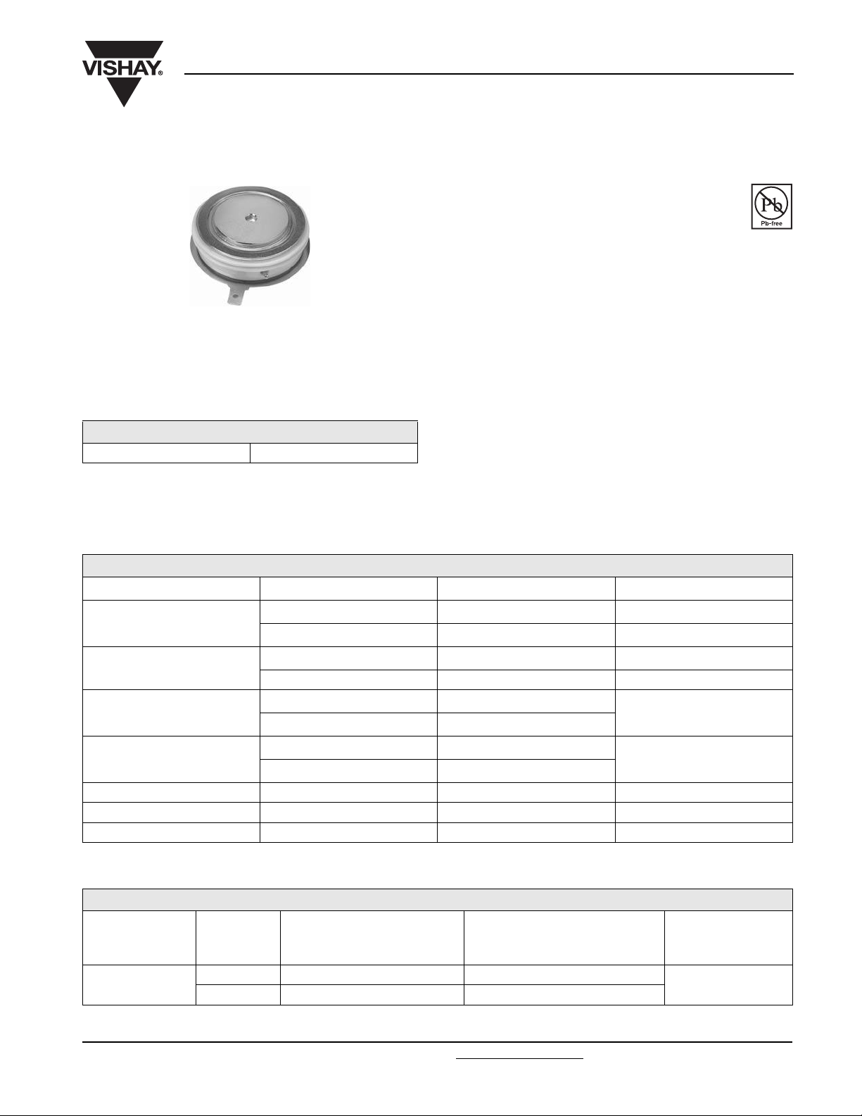
(Hockey PUK Version), 720 A
TO-200AB (E-PUK)
Vishay High Power Products
Inverter Grade Thyristors
FEATURES
• Metal case with ceramic insulator
• All diffused design
• Center amplifying gate
• Guaranteed high dV/dt
• Guaranteed high dI/dt
• International standard case TO-200AB (E-PUK)
• High surge current capability
• Low thermal impedance
• High speed performance
• Lead (Pb)-free
ST333C..C Series
RoHS
COMPLIANT
PRODUCT SUMMARY
I
T(AV)
720 A
TYPICAL APPLICATIONS
•Inverters
• Choppers
• Induction heating
• All types of force-commutated converters
MAJOR RATINGS AND CHARACTERISTICS
PARAMETER TEST CONDITIONS VALUES UNITS
I
T(AV)
I
T(RMS)
I
TSM
2
I
t
V
DRM/VRRM
t
q
T
J
T
hs
T
hs
50 Hz 11 000
60 Hz 11 500
50 Hz 605
60 Hz 553
Range 10 to 30 µs
720 A
55 °C
1435 A
25 °C
A
kA2s
400 to 800 V
- 40 to 125 °C
ELECTRICAL SPECIFICATIONS
VOLTAGE RATINGS
V
TYPE NUMBER
ST333C..C
Document Number: 93678 For technical questions, contact: ind-modules@vishay.com
Revision: 15-May-08 1
VOLTAGE
CODE
04 400 500
08 800 900
DRM/VRRM
REPETITIVE PEAK VOLTAGE
, MAXIMUM
V
V
, MAXIMUM
NON-REPETITIVE PEAK VOLTAGE
RSM
V
I
DRM/IRRM
= TJ MAXIMUM
AT T
J
www.vishay.com
MAXIMUM
mA
50
Page 3
ST333C..C Series
Vishay High Power Products
Inverter Grade Thyristors
(Hockey PUK Version), 720 A
CURRENT CARRYING CAPABILITY
I
FREQUENCY UNITS
180° el
TM
180° el
50 Hz 1630 1420 2520 2260 7610 6820
400 Hz 1630 1390 2670 2330 4080 3600
1000 Hz 1350 1090 2440 2120 2420 2100
2500 Hz 720 550 1450 1220 1230 1027
Recovery voltage V
r
Voltage before turn-on V
d
50 50 50
V
DRM
Rise of on-state current dI/dt 50 - - A/µs
Heatsink temperature 40 55 40 55 40 55 °C
Equivalent values for RC circuit 10/0.47 10/0.47 10/0.47 Ω/µF
ON-STATE CONDUCTION
PARAMETER SYMBOL TEST CONDITIONS VALUES UNITS
Maximum average on-state current
at heatsink temperature
Maximum RMS on-state current I
I
T(RMS)
Maximum peak, one half cycle,
non-repetitive surge current
Maximum I
Maximum I
2
t for fusing I2t
2
√t for fusing I2√t t = 0.1 to 10 ms, no voltage reapplied 6050 kA2√s
Maximum peak on-state voltage V
High level value of threshold voltage V
Low level value of forward slope resistance r
High level value of forward slope resistance r
Maximum holding current I
Typical latching current I
T(AV)
I
TSM
TM
T(TO)1
T(TO)2
t1
t2
H
L
180° conduction, half sine wave
Double side (single side) cooled
DC at 25 °C heatsink temperature double side cooled 1435
t = 10 ms
t = 8.3 ms 11 500
t = 10 ms
t = 8.3 ms 9700
t = 10 ms
t = 8.3 ms 553
t = 10 ms
t = 8.3 ms 391
No voltage
reapplied
100 % V
reapplied
No voltage
reapplied
100 % V
reapplied
ITM = 1810 A, TJ = TJ maximum, tp = 10 ms sine wave pulse 1.96
(16.7 % x π x I
(I > π x I
T(AV)
(16.7 % x π x I
(I > π x I
T(AV)
< I < π x I
T(AV)
), TJ = TJ maximum 0.93
< I < π x I
T(AV)
), TJ = TJ maximum 0.58
TJ = 25 °C, IT > 30 A 600
TJ = 25 °C, VA = 12 V, Ra = 6 Ω, IG = 1 A 1000
V
DRM
I
TM
RRM
Sinusoidal half wave,
initial T
RRM
), TJ = TJ maximum 0.91
T(AV)
), TJ = TJ maximum 0.58
T(AV)
100 µs
V
DRM
= TJ maximum
J
I
TM
720 (350) A
55 (75) °C
11 000
9250
605
428
A
V
A
kA2s
VLow level value of threshold voltage V
mΩ
mA
SWITCHING
PARAMETER SYMBOL TEST CONDITIONS
Maximum non-repetitive rate of rise
of turned on current
Typical delay time t
dI/dt T
d
= TJ maximum, V
J
TJ = 25 °C, VDM = Rated V
= Rated V
DRM
; ITM = 2 x dI/dt 1000 A/µs
DRM
, ITM = 50 A DC, tp = 1 µs
DRM
Resistive load, gate pulse: 10 V, 5 Ω source
TJ = TJ maximum,
= 550 A, commutating dI/dt = 40 A/µs
Maximum turn-off time t
q
I
TM
V
= 50 V, tp = 500 µs, dV/dt: See table in device code
R
www.vishay.com For technical questions, contact: ind-modules@vishay.com
2 Revision: 15-May-08
VALUES
MIN. MAX.
UNITS
1.1
µs
10 30
Document Number: 93678
Page 4

ST333C..C Series
Inverter Grade Thyristors
Vishay High Power Products
(Hockey PUK Version), 720 A
BLOCKING
PARAMETER SYMBOL TEST CONDITIONS VALUES UNITS
= TJ maximum, linear to 80 % V
T
Maximum critical rate of rise of off-state voltage dV/dt
I
Maximum peak reverse and off-state leakage current
RRM
I
DRM
,
J
higher value available on request
TJ = TJ maximum, rated V
DRM/VRRM
TRIGGERING
PARAMETER SYMBOL TEST CONDITIONS VALUES UNITS
Maximum peak gate power P
Maximum average gate power P
Maximum peak positive gate current I
Maximum peak positive gate voltage + V
Maximum peak negative gate voltage - V
Maximum DC gate currrent required to trigger I
Maximum DC gate voltage required to trigger V
Maximum DC gate current not to trigger I
Maximum DC gate voltage not to trigger V
GM
G(AV)
GM
GM
GM
GT
GT
GD
GD
TJ = TJ maximum, f = 50 Hz, d% = 50
TJ = TJ maximum, tp ≤ 5 ms
TJ = 25 °C, VA = 12 V, Ra = 6 Ω
TJ = TJ maximum, rated V
DRM
applied
,
DRM
500 V/µs
applied 50 mA
60
10
10 A
20
5
200 mA
3V
20 mA
0.25 V
W
V
THERMAL AND MECHANICAL SPECIFICATIONS
PARAMETER SYMBOL TEST CONDITIONS VALUES UNITS
Maximum operating temperature range T
Maximum storage temperature range T
Maximum thermal resistance, junction to heatsink R
Maximum thermal resistance, case to heatsink R
J
Stg
thJ-hs
thC-hs
DC operation single side cooled 0.09
DC operation double side cooled 0.04
DC operation single side cooled 0.020
DC operation double side cooled 0.010
Mounting force, ± 10 %
Approximate weight 83 g
Case style See dimensions - link at the end of datasheet TO-200AB (E-PUK)
ΔR
CONDUCTION
thJ-hs
CONDUCTION ANGLE
SINUSOIDAL CONDUCTION RECTANGULAR CONDUCTION
SINGLE SIDE DOUBLE SIDE SINGLE SIDE DOUBLE SIDE
TEST CONDITIONS UNITS
180° 0.010 0.011 0.007 0.007
120° 0.012 0.012 0.012 0.013
90° 0.015 0.015 0.016 0.017
T
60° 0.022 0.022 0.023 0.023
30° 0.036 0.036 0.036 0.037
Note
• The table above shows the increment of thermal resistance R
when devices operate at different conduction angles than DC
thJ-hs
- 40 to 125
- 40 to 150
9800
(1000)
= TJ maximum K/W
J
°C
K/W
N
(kg)
Document Number: 93678 For technical questions, contact: ind-modules@vishay.com
www.vishay.com
Revision: 15-May-08 3
Page 5

ST333C..C Series
Vishay High Power Products
130
120
110
100
90
80
70
60
50
40
30
20
0 100 200 30 0 40 0 5 0 0 600
Maximum Allowable Heatsink Temperature (°C)
Fig. 1 - Current Ratings Characteristics
130
120
110
100
90
80
70
60
50
40
30
20
0 100 200 300 400 500 600 700 800 900
Maximum A llowable Heatsink Temperature (°C)
Fig. 2 - Current Ratings Characteristics
ST333C..C Series
(Single Side Coo led)
R ( D C) = 0 .09 K / W
th J-hs
Conduction Angle
30°
60°
90°
120°
Average On-state Current (A)
ST333C ..C S eries
(Single S ide C oo led)
R ( D C) = 0.09 K/W
th J-hs
Cond uc tion Pe riod
30°
60°
90°
120°
180°
A ve ra g e O n -sta te C u rre n t (A )
DC
Inverter Grade Thyristors
(Hockey PUK Version), 720 A
130
120
110
100
180°
Maximum Allowable Heatsink Temperature (°C)
2200
2000
1800
1600
1400
1200
1000
Maximum Average On-state Power Loss (W)
ST333C..C Series
( Double Side C ooled )
R (DC) = 0.04 K/W
th J-hs
90
80
70
60
50
40
30
20
30°
60°
90°
0 200 400 600 800 10001200 1400 1600
Average On-state Current (A)
Conduction Period
120°
180°
DC
Fig. 4 - Current Ratings Characteristics
180°
120°
90°
60°
30°
800
600
400
200
0
0 200 400 600 800 1000
Averag e O n-state C urren t (A)
RMS Limit
Conduction Angle
ST333 C..C Ser ies
T = 125°C
J
Fig. 5 - On-State Power Loss Characteristics
130
120
110
100
90
80
70
60
50
40
30
20
10
0 200 400 600 800 1 00 0
Maximum Allowable Heatsink Temperature (°C)
ST333 C..C Ser ies
(D o uble Side C oo le d )
R (D C ) = 0.04 K/W
thJ-h s
Conduction Angle
30°
60°
90°
Averag e O n-state C urrent (A )
Fig. 3 - Current Ratings Characteristics
120°
180°
2600
2400
DC
180°
2200
120°
2000
90°
1800
60°
1600
30°
1400
1200
1000
800
600
400
200
0
M ax im um Ave rage On-state P ow er Loss (W )
0 200 400 600 800 1000 1200 1400 1600
Averag e O n-state C urrent (A)
RMS Limit
Conduction Period
ST333C..C Series
T = 125°C
J
Fig. 6 - On-State Power Loss Characteristics
www.vishay.com For technical questions, contact: ind-modules@vishay.com
Document Number: 93678
4 Revision: 15-May-08
Page 6

ST333C..C Series
Inverter Grade Thyristors
(Hockey PUK Version), 720 A
10000
At An y Rated Loa d Con dition An d W ith
9500
9000
8500
8000
7500
7000
6500
6000
5500
5000
Peak Half Sine Wave On-state Current (A)
4500
Number O f Eq ual Amplitude Half Cycle Current Pulses (N)
Fig. 7 - Maximum Non-Repetitive Surge Current
12000
11000
10000
Peak Half Sine Wave On-state Current (A)
Fig. 8 - Maximum Non-Repetitive Surge Current
Rated V Applied Following Surge.
RRM
ST333C..C Series
In it i a l T = 1 2 5 °C
J
@ 60 H z 0.0083 s
@ 50 H z 0.0100 s
Single and Double Side Cooled
Max imum N on Repetitive Surg e Current
Versus Pulse Train Duration. C ontrol
Of Conduction May Not Be Maintained.
9000
8000
7000
6000
ST333C..C Series
5000
4000
0.01 0.1 1
Pulse T rain Duration (s)
Initial T = 125°C
No Voltage Reapplied
Rated V Reapplied
J
RRM
Single and Double Side Cooled
Vishay High Power Products
0.1
ST333C ..C Series
thJ-h s
0.01
0.001
Tran sient The rm al Im peda nce Z (K/W )
001011
0.001 0.01 0.1 1 10
Sq ua re W a ve P u ls e D u r at io n ( s)
Fig. 10 - Thermal Impedance Z
320
300
280
260
240
220
200
180
160
140
120
100
80
10 20 30 40 50 60 70 80 90 100
Maximum R everse Recovery Charg e - Q rr (µC)
Rate Of Fall Of On-state Current - di/dt (A/µs)
Fig. 11 - Reverse Recovered Charge Characteristics
Steady State Value
R = 0 . 0 9 K /W
(Single Side Coo led )
R = 0 . 0 4 K /W
(D o uble S id e C o oled )
(D C O p e ration)
I = 500 A
TM
300 A
200 A
100 A
50 A
th J -h s
thJ-h s
Characteristics
thJ-hs
ST333C..C Series
T = 125 °C
J
10000
T = 25°C
100 0
Instantaneous On-state Current (A)
100
0.5 1 1.5 2 2.5 3 3.5 4 4.5 5 5.5 6 6.5
Insta n tan e ous O n-s tate Voltage (V)
J
T = 125°C
J
ST3 33C. .C Serie s
Fig. 9 - On-State Voltage Drop Characteristics
180
160
140
120
100
80
60
40
20
M ax im u m R eve rse R e c o ve ry C u rre n t - Irr (A )
10 20 30 40 50 60 70 80 90 100
Ra te O f Fa ll O f Fo rw ard C urren t - d i/d t (A /µs)
I = 5 00 A
TM
300 A
200 A
100 A
50 A
ST333C ..C S eries
T = 1 2 5 ° C
J
Fig. 12 - Reverse Recovery Current Characteristics
Document Number: 93678 For technical questions, contact: ind-modules@vishay.com
www.vishay.com
Revision: 15-May-08 5
Page 7

ST333C..C Series
Vishay High Power Products
1E4
400
500
1000
1500
5000
2500
3000
Pulse Basewidth (µs)
2500
3000
5000
Pulse Basewidth (µs)
200 0
1500
1000
500
tp
400
tp
ST333C..C Series
Trapezoid al p ulse
T = 40°C
C
di/d t = 50A/µs
1E3
Peak On-st ate Current (A)
1E2
1E1 1E2 1E3 1E4
1E4
1E3
Peak On-state C urrent (A)
1E2
1E1 1E2 1E3 1E4
Inverter Grade Thyristors
(Hockey PUK Version), 720 A
200
ST333C..C Series
Sinusoidal pulse
T = 40°C
200
Snubbe r circuit
R = 10 ohm s
C = 0.47 µF
V = 80% V
50 H z
100
Snubb er circu it
R = 10 ohm s
s
C = 0.47 µF
s
V = 80% V
C
DRM
D
Fig. 13 - Frequency Characteristics
50 H z
100
s
s
D DRM
1E1 1E2 1E3 1E4
Snubber circuit
R = 10 ohm s
s
C = 0.47 µF
s
V = 80% V
D
1E11E21E31E4
400
200
500
1000
150 0
2500
3000
5000 ST333C..C Serie s
tp
100
50 Hz
Snubb er circuit
R = 10 ohm s
s
C = 0.47 µF
s
V = 80% V
D
DRM
Sinusoidal pulse
T = 55°C
C
Pulse B a sew idth (µs)
DRM
5000
3000
2500
2000
1500
1000
400
500
ST333C..C Series
Tr a p ezo id a l p uls e
T = 55°C
tp
di/d t = 1 00A/µ s
200
C
100
50 H z
Pulse Basewidth (µs)
Fig. 14 - Frequency Characteristics
1E4
100
200
400
500
1000
1E3
Pea k O n- sta te C u rre nt (A )
1E2
1E1 1E2 1E3 1E4
5000
1500
2000
2500
3000
ST333C..C Series
Trapezoidal pulse
T = 40°C
tp
d i/dt = 100A/µ s
Snubb er circuit
R = 10 ohms
s
C = 0.47 µF
s
V = 80% V
D
C
Pu lse B asew idt h (µs)
50 Hz
DRM
Snubber circuit
R = 10 ohm s
s
C = 0.47 µF
s
V = 80% V
DR M
D
200
400
500
100 0
1500
2000
2500
3000
5000
ST333C..C Series
Tr a p ezo id a l p uls e
T = 55°C
tp
di/d t = 10 0A/µ s
50 Hz
100
C
1E1 1E 2 1 E3 1 E4
Pulse Basew idth (µs)
Fig. 15 - Frequency Characteristics
www.vishay.com For technical questions, contact: ind-modules@vishay.com
Document Number: 93678
6 Revision: 15-May-08
Page 8

ST333C..C Series
Inverter Grade Thyristors
(Hockey PUK Version), 720 A
1E4
1E3
0.5
0.3
0.2
1E2
Peak On-state C urrent (A)
1E1
1E1 1E2 1E3 1E4
ST33 3C ..C Se ries
Sinusoidal pulse
tp
Pulse Basew idth (µs)
100
Rectangular gate pulse
a ) Re c om m e n d e d lo a d lin e fo r
rated di/dt : 20V, 10ohm s; tr<=1 µs
b ) Re c o m m en d e d lo a d lin e f o r
<=30% rated di/dt : 10V, 10ohms
10
tr<=1 µs
1
Insta n tan e ou s G ate Vo ltage (V)
0.1
0.001 0.01 0.1 1 10 100
20 joule s pe r pu lse
10
5
3
2
1
Fig. 16 - Maximum On-State Energy Power Loss Characteristics
VGD
IG D
Vishay High Power Products
ST3 3 3 C Se r ies
Re c t a ng ula r puls e
di/dt = 50A/µs
t p
0.3
0.2
1E4
(b)
Tj=25 °C
Tj=125 °C
Device: ST333C..C Series Freq uen cy Lim ite d by PG (AV )
Instan tane ous G ate C urr en t (A )
1E1 1E2 1E3 1E4
Pulse Basew idth (µs)
(1) PGM = 1 0W , tp = 20m s
(2) PGM = 2 0W , tp = 10m s
(3) PGM = 4 0W , tp = 5m s
(4) PGM = 60W, tp = 3.3m s
(a)
Tj=-40 °C
(2)
(1)
(3 )
0.4
(4)
0.5
10
5
3
2
1
20 joules per pulse
Fig. 17 - Gate Characteristics
Document Number: 93678 For technical questions, contact: ind-modules@vishay.com
www.vishay.com
Revision: 15-May-08 7
Page 9

ST333C..C Series
Vishay High Power Products
ORDERING INFORMATION TABLE
Device code
ST 33 3 C 08 C H K 1 -
324
1 - Thyristor
2 - Essential part number
3 - 3 = Fast turn off
4 - C = Ceramic PUK
5 - Voltage code x 100 = V
6 - C = PUK case TO-200AB (E-PUK)
7 - Reapplied dV/dt code (for t
8 -t
9 - 0 = Eyelet term.
code
q
(gate and aux. cathode unsoldered leads)
1 = Fast-on term.
(gate and aux. cathode unsoldered leads)
2 = Eyelet term.
(gate and aux. cathode soldered leads)
3 = Fast-on term.
(gate and aux. cathode soldered leads)
Inverter Grade Thyristors
(Hockey PUK Version), 720 A
51
678910
(see Voltage Ratings table)
RRM
test condition)
q
dV/dt - t
dV/dt (V/µs)
tq (µs)
* Standard part number.
All other types available only on request.
combinations available
q
20 50 100 200 400
10 CN DN EN -- -12 CM DM EM FM* -15 CL DL EL FL* HL
18 CP DP EP FP HP
20 CK DK EK FK HK
25 -- -- -- FJ HJ
30 -- -- -- -- HH
- Critical dV/dt:
10
None = 500 V/µs (standard value)
L = 1000 V/µs (special selection)
LINKS TO RELATED DOCUMENTS
Dimensions http://www.vishay.com/doc?95075
www.vishay.com For technical questions, contact: ind-modules@vishay.com
8 Revision: 15-May-08
Document Number: 93678
 Loading...