

Page 1

6121 Baker Road,
Suite 108
Minnetonka, MN 55345
www.chtechnology.com
Phone (952) 933-6190
Fax (952) 933-6223
1-800-274-4284
Thank you for downloading this document from C&H Technology, Inc.
Please contact the C&H Technology team for the following questions -
Technical
Application
Assembly
Availability
Pricing
Phone – 1-800-274-4284
E-Mail – sales@chtechnology.com
www.chtechnology.com - SPECIALISTS IN POWER ELECTRONIC COMPONENTS AND ASSEMBLIES - www.chtechnology.com
Page 2
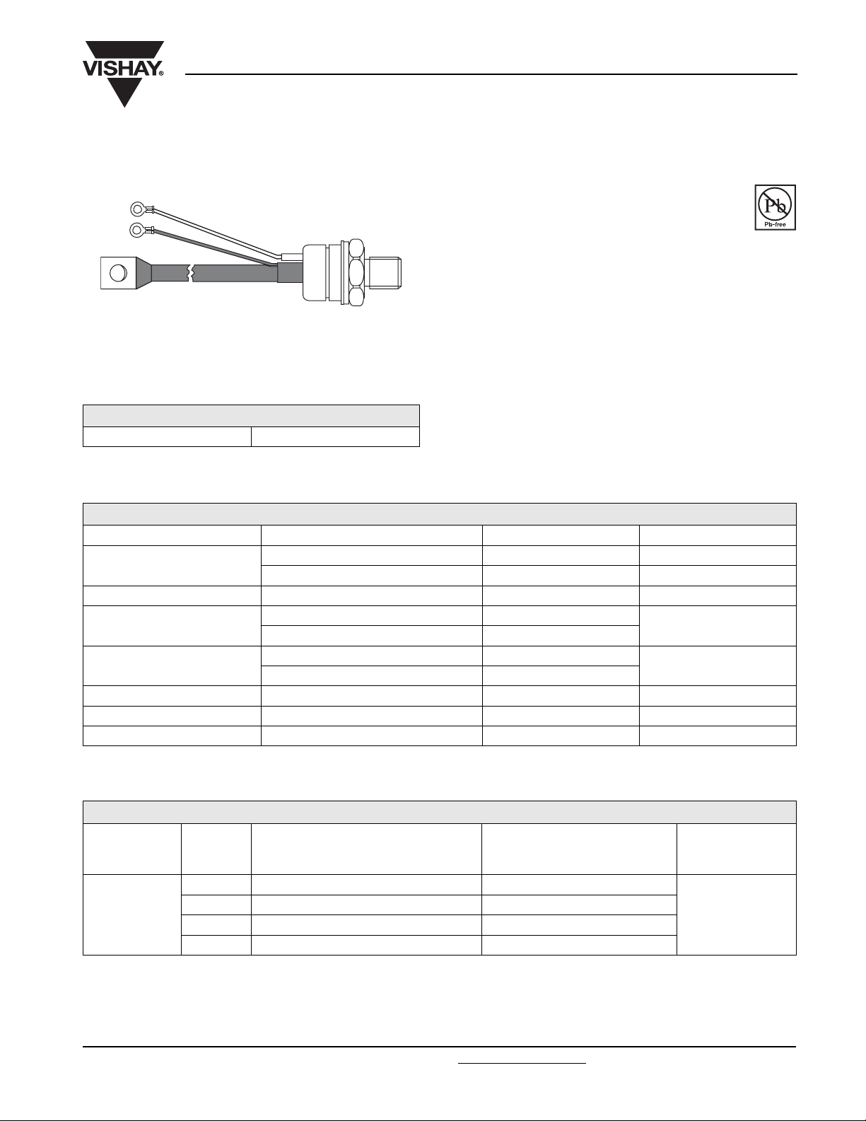
TO-209AB (TO-93)
PRODUCT SUMMARY
I
T(AV)
Vishay High Power Products
Phase Control Thyristors
(Stud Version), 230 A
FEATURES
• Center amplifying gate
• International standard case TO-209AB (TO-93)
• Hermetic metal case with ceramic insulator
(Also available with glass-metal seal up to 1200 V)
• Compression bonded encapsulation for heavy duty
operations such as severe thermal cycling
• Lead (Pb)-free
• Designed and qualified for industrial level
TYPICAL APPLICATIONS
• DC motor controls
230 A
• Controlled DC power supplies
• AC controllers
ST230SPbF Series
RoHS
COMPLIANT
MAJOR RATINGS AND CHARACTERISTICS
PARAMETER TEST CONDITIONS VALUES UNITS
I
T(AV)
I
T(RMS)
I
TSM
2
I
t
V
DRM/VRRM
t
q
T
J
T
C
50 Hz 5700
60 Hz 5970
50 Hz 163
60 Hz 149
Typical 100 µs
230 A
85 °C
360 A
400 to 1600 V
- 40 to 125 °C
ELECTRICAL SPECIFICATIONS
VOLTAGE RATINGS
TYPE NUMBER
ST230S
V
VOLTAGE
CODE
04 400 500
08 800 900
12 1200 1300
16 1600 1700
DRM/VRRM
PEAK AND OFF-STATE VOLTAGE
, MAXIMUM REPETITIVE
V
V
, MAXIMUM NON-REPETITIVE
RSM
PEAK VOLTAGE
V
I
DRM/IRRM
AT T
A
kA2s
MAXIMUM
= TJ MAXIMUM
J
mA
30
Document Number: 94399 For technical questions, contact: ind-modules@vishay.com
Revision: 05-May-08 1
www.vishay.com
Page 3
ST230SPbF Series
Vishay High Power Products
Phase Control Thyristors
(Stud Version), 230 A
ON-STATE CONDUCTION
PARAMETER SYMBOL TEST CONDITIONS VALUES UNITS
Maximum average on-state current
at case temperature
Maximum RMS on-state current I
I
T(RMS)
Maximum peak, one-cycle
non-repetitive surge current
2
Maximum I
Maximum I
t for fusing I2t
2
√t for fusing I2√t t = 0.1 to 10 ms, no voltage reapplied 1630 kA2√s
Low level value of threshold voltage V
High level value of threshold voltage V
Low level value of on-state slope resistance r
High level value of on-state slope resistance r
Maximum on-state voltage V
Maximum holding current I
Maximum (typical) latching current I
T(AV)
180° conduction, half sine wave
DC at 78 °C case temperature 360
I
TSM
T(TO)1
T(TO)2
t1
t2
TM
H
L
t = 10 ms
t = 8.3 ms 5970
t = 10 ms
t = 8.3 ms 5000
t = 10 ms
t = 8.3 ms 148
t = 10 ms
t = 8.3 ms 105
(16.7 % x π x I
(I > π x I
(16.7 % x π x I
(I > π x I
Ipk = 720 A, TJ = TJ maximum, tp = 10 ms sine pulse 1.55 V
TJ = 25 °C, anode supply 12 V resistive load
No voltage
reapplied
100 % V
reapplied
No voltage
RRM
Sinusoidal half wave,
initial T
= TJ maximum
J
reapplied
100 % V
RRM
reapplied
< I < π x I
T(AV)
), TJ = TJ maximum 0.98
T(AV)
< I < π x I
T(AV)
), TJ = TJ maximum 0.81
T(AV)
), TJ = TJ maximum 0.92
T(AV)
), TJ = TJ maximum 0.88
T(AV)
230 A
85 °C
5700
4800
163
115
600
1000 (300)
A
kA2s
V
mΩ
mA
SWITCHING
PARAMETER SYMBOL TEST CONDITIONS VALUES UNITS
Maximum non-repetitive rate of rise
of turned-on current
Typical delay time t
Typical turn-off time t
dI/dt
d
q
Gate drive 20 V, 20 Ω, t
T
= TJ maximum, anode voltage ≤ 80 % V
J
≤ 1 µs
r
DRM
Gate current 1 A, dIg/dt = 1 A/µs
V
= 0.67 % V
d
, TJ = 25 °C
DRM
ITM = 300 A, TJ = TJ maximum, dI/dt = 20 A/µs,
V
= 50 V, dV/dt = 20 V/µs, gate 0 V 100 Ω, tp = 500 µs
R
1000 A/µs
1.0
µs
100
BLOCKING
PARAMETER SYMBOL TEST CONDITIONS VALUES UNITS
Maximum critical rate of rise
of off-state voltage
Maximum peak reverse and
off-state leakage current
dV/dt T
,
I
RRM
I
DRM
= TJ maximum linear to 80 % rated V
J
TJ = TJ maximum, rated V
DRM/VRRM
DRM
500 V/µs
applied 30 mA
www.vishay.com For technical questions, contact: ind-modules@vishay.com
Document Number: 94399
2 Revision: 05-May-08
Page 4
ST230SPbF Series
Phase Control Thyristors
Vishay High Power Products
(Stud Version), 230 A
TRIGGERING
PARAMETER SYMBOL TEST CONDITIONS
Maximum peak gate power P
Maximum average gate power P
Maximum peak positive gate current I
Maximum peak positive gate voltage + V
Maximum peak negative gate voltage - V
GM
G(AV)
GM
GM
GM
TJ = TJ maximum, tp ≤ 5 ms 10.0
TJ = TJ maximum, f = 50 Hz, d% = 50 2.0
TJ = TJ maximum, tp ≤ 5 ms 3.0 A
TJ = TJ maximum, tp ≤ 5 ms
TJ = - 40 °C
DC gate current required to trigger I
DC gate voltage required to trigger V
DC gate current not to trigger I
DC gate voltage not to trigger V
GT
GD
GT
GD
T
= 25 °C 90 150 mA
J
T
= 125 °C 40 -
J
TJ = - 40 °C 2.9 -
= 25 °C 1.8 3.0
T
J
T
= 125 °C 1.2 -
J
TJ = TJ maximum
Maximum required gate
trigger/current/voltage are
the lowest value which will
trigger all units 12 V anode
to cathode applied
Maximum gate current/
voltage not to trigger is the
maximum value which will
not trigger any unit with rated
V
anode to cathode applied
DRM
VALUES
TYP. MAX.
20
5.0
180 -
10 mA
0.25 V
UNITS
W
V
V
THERMAL AND MECHANICAL SPECIFICATIONS
PARAMETER SYMBOL TEST CONDITIONS VALUES UNITS
Maximum operating junction
temperature range
Maximum storage temperature range T
Maximum thermal resistance,
junction to case
Maximum thermal resistance,
case to heatsink
R
T
R
thJC
thC-hs
J
Stg
DC operation 0.10
Mounting surface, smooth, flat and greased 0.04
Non-lubricated threads
Mounting torque, ± 10 %
Lubricated threads
Approximate weight 280 g
Case style See dimensions - link at the end of datasheet TO-209AB (TO-93)
ΔR
CONDUCTION
thJC
CONDUCTION ANGLE SINUSOIDAL CONDUCTION RECTANGULAR CONDUCTION TEST CONDITIONS UNITS
180° 0.016 0.012
120° 0.019 0.020
90° 0.025 0.027
T
60° 0.036 0.037
30° 0.060 0.060
Note
Document Number: 94399 For technical questions, contact: ind-modules@vishay.com
Revision: 05-May-08 3
- 40 to 125
- 40 to 150
K/W
31
(275)
24.5
N · m
(lbf ⋅ in)
(210)
= TJ maximum K/W
J
www.vishay.com
°C
Page 5

ST230SPbF Series
Vishay High Power Products
Phase Control Thyristors
(Stud Version), 230 A
• The table above shows the increment of thermal resistance R
130
120
110
100
90
80
Maximum Allowable Case Temperature (°C)
050100150200250
Fig. 1 - Current Ratings Characteristics Fig. 2 - Current Ratings Characteristics
ST2 30 S Se r i e s
R (DC) = 0.1 K/ W
thJC
Cond uction Ang le
90°
30°
60°
120°
Averag e On-state Current (A)
350
300
250
200
180°
120°
90°
60°
30°
RM S Li m i t
150
100
50
180°
Conduc tion Angle
ST2 30 S Se r ie s
T = 12 5 ° C
J
when devices operate at different conduction angles than DC
thJC
130
120
ST2 30 S Se ri e s
R (DC) = 0.1 K/ W
thJC
110
Conduc tion Period
100
90
30°
80
70
Maximum Allowa ble Case Tem perature (°C)
0 100 200 300 400
60°
90°
120°
180°
Average On-state Current (A)
R
t
h
S
0
0
.
1
6
0
.
2
K
/
W
0
.
3
K
/
W
0
.
4
K
/
W
0
.
5
K
/
W
0
.
8
K
/
W
1
.
2
K
/
W
A
.
1
=
K
0
/
K
/
W
.
W
0
8
K
/
W
D
e
l
t
a
R
DC
0
Maximum Average On-state Power Loss (W)
50
0
100 150 200 250
Average On-state Current (A)
25 50 75 100 125
Maximum Allowab le Ambient Temperat ure (°C)
Fig. 3 - On-State Power Loss Characteristics
450
400
350
300
250
200
150
100
50
Maximum Average On-st ate Power Loss (W)
DC
180°
120°
90°
60°
30°
RM S Li m it
Conduction Period
ST2 30 S Se ri e s
T = 125°C
J
0
0 50 100150200250300350400
Average On-state Current (A)
R
t
h
S
A
0
=
.
1
0
K
.
08
/
W
0
.
1
0
.
2
0
.
3
0
.
4
0
.
5
0
.
8
1
.
2
K/
6
K
/
K
/
K
/
K
K
K
W
K
/
W
W
W
W
/
W
/
W
/
W
-
D
e
l
t
a
R
25 50 75 100 125
Maximum Allowable Ambient Temperature (°C)
Fig. 4 - On-State Power Loss Characteristics
www.vishay.com For technical questions, contact: ind-modules@vishay.com
Document Number: 94399
4 Revision: 05-May-08
Page 6

ST230SPbF Series
Phase Control Thyristors
Vishay High Power Products
(Stud Version), 230 A
5500
At Any Rated Lo ad Co ndition And With
Rated V Applied Following Surge.
5000
4500
4000
3500
3000
2500
Peak Half Sine Wave On -st ate Curren t ( A)
2000
110100
Number Of Eq ual Amplitude Half Cycle Current Pulses (N)
RRM
ST2 30 S Se r i e s
Init ial T = 125°C
J
@ 60 Hz 0.0083 s
@ 50 Hz 0.0100 s
Fig. 5 - Maximum Non-Repetitive Surge Current Fig. 6 - Maximum Non-Repetitive Surge Current
10000
6000
Maximum Non Repetitive Surge Current
Versus Pulse Train Durat ion . Cont rol
Of Cond uct ion May Not Be Maintained.
ST2 30 S Se ri e s
0.01 0. 1 1
Pul se Tra in Dur at io n ( s)
Init ia l T = 125°C
No V olt ag e Re a p plied
Rate d V Rea pp lied
RRM
Peak Half Sine Wave On-state Current (A)
5500
5000
4500
4000
3500
3000
2500
2000
J
1
thJC
0.1
0.01
1000
100
Instantaneous On-state Current (A)
10
Fig. 7 - On-State Voltage Drop Characteristics
St e a d y St a t e V a l u e
R = 0.1 K/W
thJC
(DC Operation)
Tj = 25˚C
Tj = 125˚C
ST230S Series
0.5 1.5 2.5 3.5 4.5
Instantaneous On-state Voltage (V)
ST230S Series
Tr a n si e n t Th e rm a l Im p e d a n c e Z ( K/ W )
0.001
0.001 0.01 0.1 1 10
Sq u a r e Wa v e Pu l se D u r a t i o n ( s)
Fig. 8 - Thermal Impedance Z
Characteristics
thJC
Document Number: 94399 For technical questions, contact: ind-modules@vishay.com
www.vishay.com
Revision: 05-May-08 5
Page 7

ST230SPbF Series
Vishay High Power Products
100
Rectangular gate pulse
a) Recommended load line for
rated di/dt : 20V, 10ohms; tr<=1 µs
b) Recommended load line for
<=30% rated di/dt : 10V, 10ohms
10
tr<=1 µs
1
In st a nt a n e o us G a t e Vo lt a g e ( V )
0.1
0.001 0.01 0.1 1 10 100
ORDERING INFORMATION TABLE
Device code
ST 23 0 S 16 P 0 V PbF
VGD
Phase Control Thyristors
(Stud Version), 230 A
(a)
(b)
Tj = - 40 ° C
Tj = 25 ° C
Tj =1 2 5 ° C
IGD
Devic e: ST230S Serie s
Instantaneous Gate Current (A)
Fig. 9 - Gate Characteristics
Frequency Limited by PG(AV)
(1) PGM = 10W, tp = 4ms
(2) PGM = 20W, tp = 2ms
(3) PGM = 40W, tp = 1ms
(4) PGM = 60W, t p = 0.66ms
(1) (2)
(3)
(4)
324
1
- Thyristor
2
- Essential part number
3
- 0 = Converter grade
4
- S = Compression bonding stud
5
- Voltage code x 100 = V
6
- P = Stud base 3/4"-16UNF2A threads
7
- 0 = Eyelet terminals (gate and auxiliary cathode leads)
51
6789
(see Voltage Ratings table)
RRM
1 = Fast-on terminals (gate and auxiliary cathode leads)
8
-
V = Glass-metal seal (only up to 1200 V)
None = Ceramic housing (over 1200 V)
- Lead (Pb)-free
9
Note: For metric device M16 x 1.5 contact factory
LINKS TO RELATED DOCUMENTS
Dimensions http://www.vishay.com/doc?95077
www.vishay.com For technical questions, contact: ind-modules@vishay.com
6 Revision: 05-May-08
Document Number: 94399
 Loading...