

Vishay High Power Products
Fast Recovery Diodes
(Hockey PUK Version), 600 A
FEATURES
• High power FAST recovery diode series
SD603C..C Series
• 1.0 to 2.0 µs recovery time
• High voltage ratings up to 2200 V
• High current capability
B-43
• Optimized turn-on and turn-off characteristics
• Low forward recovery
• Fast and soft reverse recovery
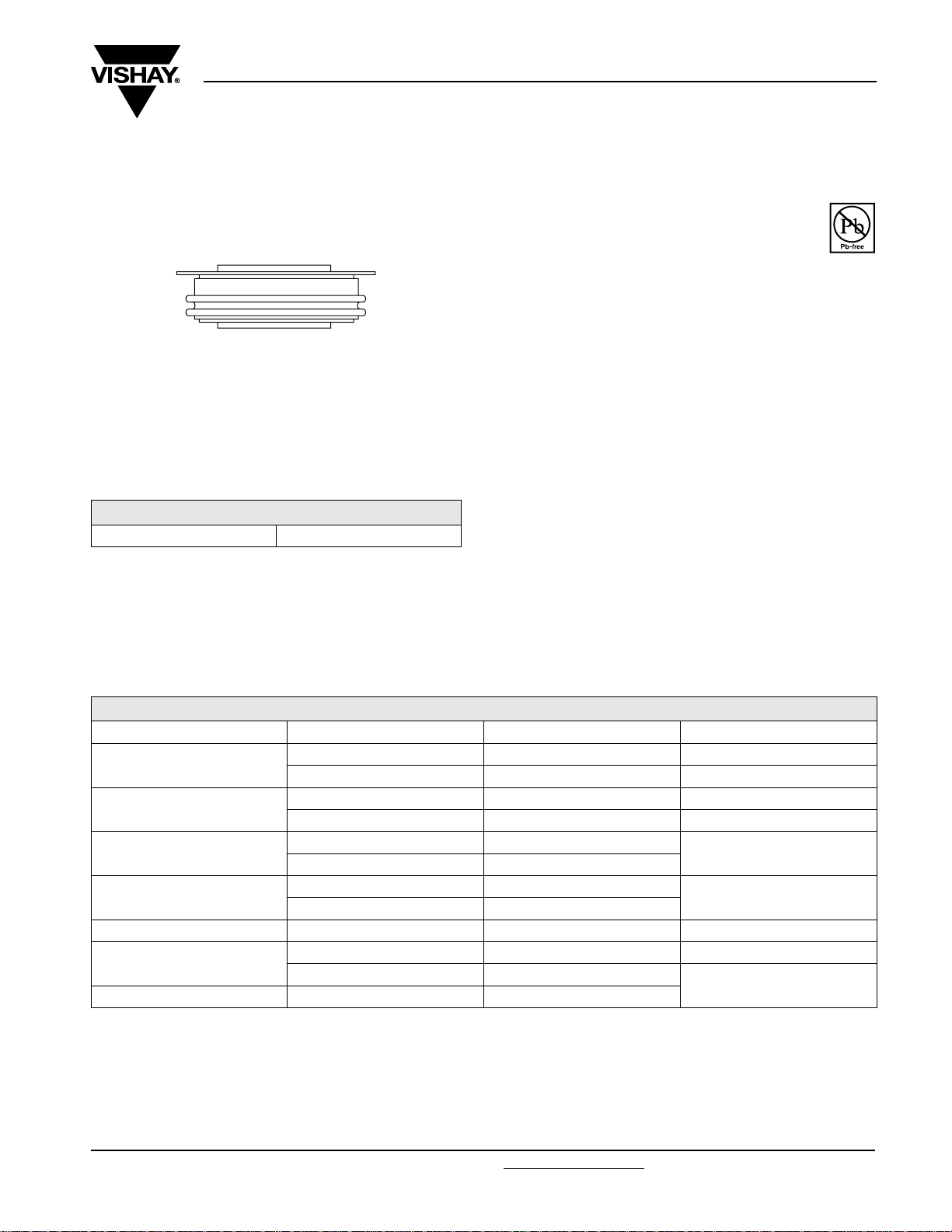
• Press PUK encapsulation
• Case style conform to JEDEC B-43
• Maximum junction temperature 125 °C
• Lead (Pb)-free
PRODUCT SUMMARY
I
F(AV)
600 A
• Designed and qualified for industrial level
TYPICAL APPLICATIONS
• Snubber diode for GTO
• High voltage freewheeling diode
• Fast recovery rectifier applications
MAJOR RATINGS AND CHARACTERISTICS
PARAMETER TEST CONDITIONS VALUES UNITS
I
F(AV)
I
F(RMS)
I
FSM
2
t
I
V
RRM
t
rr
T
J
T
hs
T
hs
50 Hz 8320
60 Hz 8715
50 Hz 346
60 Hz 316
Range 400 to 2200 V
T
J
600 A
55 °C
942 A
25 °C
1.0 to 2.0 µs
25
- 40 to 125
A
kA2s
°C
RoHS
COMPLIANT
Document Number: 93178 For technical questions, contact: ind-modules@vishay.com
Revision: 04-Aug-08 1
www.vishay.com
SD603C..C Series
Vishay High Power Products
Fast Recovery Diodes
(Hockey PUK Version), 600 A
ELECTRICAL SPECIFICATIONS
VOLTAGE RATINGS
V
, MAXIMUM REPETITIVE PEAK
TYPE NUMBER
VOLTAGE
CODE
RRM
AND OFF-STATE VOLTAGE
V
04 400 500
SD603C..S10C
08 800 900
10 1000 1100
12 1200 1300
SD603C..S15C
14 1400 1500
16 1600 1700
SD603C..S20C
20 2000 2100
22 2200 2300
FORWARD CONDUCTION
PARAMETER SYMBOL TEST CONDITIONS VALUES UNITS
Maximum average forward current
at heatsink temperature
Maximum RMS current I
F(RMS)
Maximum peak, one-cycle
non-repetitive forward current
2
Maximum I
Maximum I
t for fusing I2t
2
√t for fusing I2√t t = 0.1 to 10 ms, no voltage reapplied 3460 kA2√s
Low level value of threshold voltage V
High level value of threshold voltage V
Low level of forward slope resistance r
High level of forward slope resistance r
Maximum forward voltage drop V
I
F(AV)
I
FSM
F(TO)1
F(TO)2
180° conduction, half sine wave
Double side (single side) cooled
25 °C heatsink temperature double side cooled 942
t = 10 ms
t = 8.3 ms 8715
t = 10 ms
t = 8.3 ms 7330
t = 10 ms
t = 8.3 ms 316
t = 10 ms
t = 8.3 ms 224
(16.7 % x π x I
(I > π x I
(16.7 % x π x I
f1
(I > π x I
f2
Ipk = 1885 A, TJ = 25 °C; tp = 10 ms sinusoidal wave 2.97 V
FM
No voltage
reapplied
100 % V
reapplied
No voltage
reapplied
100 % V
reapplied
F(AV)
), TJ = TJ maximum 1.81
F(AV)
F(AV)
), TJ = TJ maximum 0.67
F(AV)
V
RRM
RRM
< I < π x I
< I < π x I
, MAXIMUM NON-REPETITIVE
RSM
PEAK VOLTAGE
V
Sinusoidal half wave,
= TJ maximum
initial T
J
), TJ = TJ maximum 1.36
F(AV)
), TJ = TJ maximum 0.87
F(AV)
I
MAXIMUM
RRM
AT T
= 125 °C
J
mA
45
600 (300) A
55 (75) °C
8320
7000
346
245
A
kA2s
V
mΩ
RECOVERY CHARACTERISTICS
CODE
MAXIMUM VALUE
AT T
= 25 °C
J
t
AT 25 % I
rr
RRM
(µs)
TEST CONDITIONS
I
pk
SQUARE
PULSE
dI/dt
(A/µs)
V
(V)
t
r
(A)
S10 1.0
S15 1.5 3.2 87 51
1000 25 - 30
S20 2.0 3.5 97 55
www.vishay.com For technical questions, contact: ind-modules@vishay.com
2 Revision: 04-Aug-08
TYPICAL VALUES
= 125 °C
AT T
J
AT 25 % I
rr
(µs)
RRM
(µC)
2.0 45 34
I
Q
rr
I
rr
(A)
FM
t
rr
I
RM(REC)
t
Q
rr
dir
dt
Document Number: 93178
SD603C..C Series
Fast Recovery Diodes
Vishay High Power Products
(Hockey PUK Version), 600 A
THERMAL AND MECHANICAL SPECIFICATIONS
PARAMETER SYMBOL TEST CONDITIONS VALUES UNITS
Maximum operating junction
temperature range
Maximum storage temperature range T
Maximum thermal resistance,
junction to heatsink
Mounting force, ± 10 % 9800 (1000) N (kg)
Approximate weight 83 g
Case style See dimensions - link at the end of datasheet B-43
ΔR
CONDUCTION ANGLE
Note
• The table above shows the increment of thermal resistance R
CONDUCTION
thJ-hs
SINUSOIDAL CONDUCTION RECTANGULAR CONDUCTION
SINGLE SIDE DOUBLE SIDE SINGLE SIDE DOUBLE SIDE
180° 0.006 0.007 0.005 0.005
120° 0.008 0.008 0.008 0.008
90° 0.010 0.010 0.011 0.011
60° 0.015 0.015 0.016 0.015
30° 0.026 0.025 0.026 0.025
R
T
J
Stg
thJ-hs
DC operation single side cooled 0.076
DC operation double side cooled 0.038
when devices operate at different conduction angles than DC
thJ-hs
- 40 to 125
- 40 to 150
TEST CONDITIONS UNITS
= TJ maximum K/W
T
J
°C
K/W
Document Number: 93178 For technical questions, contact: ind-modules@vishay.com
Revision: 04-Aug-08 3
www.vishay.com

SD603C..C Series
Vishay High Power Products
130
120
110
100
90
80
70
0 50 100 150 200 250 300 350
Maximum Allowable Heatsink Temperat ure (°C)
Ave ra ge Fo rw a rd Cu rrent (A)
Fig. 1 - Current Ratings Characteristics
130
120
110
100
90
80
70
60
0 100 200 300 400 500
Maximum Allowa ble Heatsink Temperature (°C)
Ave rag e Forwa rd C urre nt (A)
Fig. 2 - Current Ratings Characteristics
SD 6 0 3 C . . C Se r ie s
(Single Side Cooled)
R (DC) = 0.076 K/ W
thJ-hs
Conduction Angle
60°
30°
SD 6 0 3 C . . C Se r i e s
(Single Side Cooled)
R ( DC) = 0.076 K/W
thJ-hs
30°
60°
90°
Cond uct ion Period
90°
120°
180°
120°
Fast Recovery Diodes
(Hockey PUK Version), 600 A
180°
Maximum Allowable Heatsink Temperature (°C)
DC
Maximum Average Forward Power Loss (W)
130
120
110
100
90
80
70
60
50
40
0 200 400 600 800 1000
SD603C. .C Se ries
(Double Side Cooled)
R (DC ) = 0.038 K/ W
thJ-hs
Conduction Period
30°
60°
90°
120°
180°
Average Forward Current (A)
DC
Fig. 4 - Current Ratings Characteristics
1800
1600
1400
1200
1000
800
600
400
200
0
180°
120°
90°
60°
30°
RM S Li mi t
Conduction Angle
SD603C..C Series
T = 125°C
J
0 100200300400500600
Average Forward Current (A)
Fig. 5 - Forward Power Loss Characteristics
130
120
110
100
90
80
70
60
50
0 100 200 300 400 500 600 700
Maximum Allowable Heatsink Temperature (°C)
SD 60 3 C .. C Se r ie s
(Double Side Cooled)
R (DC) = 0.038 K/W
thJ-hs
Cond uction Angle
30°
60°
90°
Ave rage Forwa rd C urre nt ( A)
Fig. 3 - Current Ratings Characteristics
120°
180°
2500
DC
180°
2000
1500
1000
Maximum Average Forward Power Loss (W)
120°
90°
60°
30°
RM S Lim i t
Cond uc tion Period
500
0
0 200 400 600 800 1000
Average Forward Current (A)
SD 6 03 C .. C Se r ie s
T = 125°C
J
Fig. 6 - Forward Power Loss Characteristics
www.vishay.com For technical questions, contact: ind-modules@vishay.com
Document Number: 93178
4 Revision: 04-Aug-08

SD603C..C Series
Fast Recovery Diodes
(Hockey PUK Version), 600 A
8000
At Any Rated Load Condition and With
7500
Ra ted V App lied Follow ing Surg e.
7000
6500
6000
5500
5000
4500
4000
3500
SD603C. .C Ser ies
3000
Pe a k Ha l f Sine Wave Forward Current (A)
2500
110100
Number of Equal Amplitude Ha lf Cycle Current Pulses (N)
Fig. 7 - Maximum Non-Repetitive Surge Current
9000
8000
7000
6000
5000
4000
3000
Pe ak Ha lf Sine Wave Forward Current (A)
2000
0.01 0.1 1
Fig. 8 - Maximum Non-Repetitive Surge Current
RRM
Init ial T = 125°C
J
@ 60 Hz 0.0083 s
@ 50 Hz 0.0100 s
Single and Double Side Cooled
Maximum Non Rep etitive Surge Current
SD 6 0 3 C . . C Se r i e s
Versus Pulse Train Duration.
Pulse Train Duration (s)
Init ia l T = 125 °C
No V o lt ag e Rea pp lie d
Rat ed V Re ap plied
RRM
J
Single and Double Side Cooled
Vishay High Power Products
10000
1000
T = 25 ° C
J
T = 125 °C
100
Instanta neous Fo rwa rd Current (A)
10
.5 1.5 2.5 3.5 4.5 5.5 6.5 7.5 8.5
Instantaneous Forward Voltage (V)
Fig. 9 - Forward Voltage Drop Characteristics
0.1
SD 6 0 3 C . . C Se r ie s
thJ-hs
0.01
0.001
Tran sie nt Th erm al Imp eda nce Z (K/ W)
0.001 0.01 0.1 1 10 100
Sq u a r e W a v e Pu l se D u ra t i o n ( s)
Fig. 10 - Thermal Impedance Z
J
SD603C..C Se ries
St e a d y St a t e V a l u e :
R = 0. 076 K/ W
thJ-hs
(Single Side Cooled)
R = 0. 038 K/ W
thJ-hs
(Double Side Cooled)
(DC Operation)
Characteristics
thJ-hs
100
V
80
60
40
Forward Recovery (V)
20
FP
0
0 200 400 600 800 100012001400160018002000
I
Ra t e Of f Ri se O f Fo rw a r d C u r re n t d i / d t ( A / u se c )
T = 12 5° C
J
T = 25 °C
J
SD 60 3 C . . S20 C Se r i e s
Fig. 11 - Typical Forward Recovery Characteristics
Document Number: 93178 For technical questions, contact: ind-modules@vishay.com
www.vishay.com
Revision: 04-Aug-08 5

SD603C..C Series
Vishay High Power Products
2.2
2.1
2
1.9
1.8
1.7
M a xi m um Re v e rse Re c o v e r y Tim e - Trr ( µ s)
1.6
Rat e Of Fa ll O f Forw a rd C urrent - d i/ dt (A/ µs)
Fig. 12 - Recovery Time Characteristics
130
120
110
100
90
80
70
60
50
40
30
20
M a xi m um Re v e r se Re c o v er y C ha rg e - Q r r ( µ C )
Ra t e O f Fa l l O f Fo r w a rd C u rr en t - d i / d t (A / µ s)
Fig. 13 - Recovery Charge Characteristics
SD603C..S10C Series
T = 125 ° C; V = 30V
J
SD 60 3C . . S1 0C Se r i e s
T = 125 °C ; V = 30V
J
10 20 30 40 50 60 70 80 90 100
r
I = 1000 A
FM
Sq u a r e Pu l se
250 A
I = 1 000 A
FM
Sq u a r e P u l se
500 A
r
500 A
250 A
Fast Recovery Diodes
(Hockey PUK Version), 600 A
00101
Rate Of Fall Of Forward Current - di/dt (A/µs)
Fig. 15 - Recovery Time Characteristics
Rate Of Fall Of Forward Current - di/d t (A/µs)
Fig. 16 - Recovery Charge Characteristics
4
SD603C ..S15C Series
T = 125 °C ; V = 30V
J
3.5
3
2.5
Ma ximum Reverse Rec overy Time - Trr (µs)
2
200
180
160
140
120
100
80
60
40
10 20 30 40 50 60 70 80 90 100
Maximum Reverse Recovery Cha rge - Qrr (µC)
I = 10 00 A
FM
Sq u a r e Pu l se
500 A
250 A
I = 1000 A
FM
Sq u a r e P u l s e
500 A
250 A
SD 60 3 C . . S1 5C Se r i e s
T = 125 °C; V = 30V
J
r
00101
r
120
110
100
90
80
70
60
50
40
30
20
10
Maximum Reverse Recovery Current - Irr (A)
Ra t e O f Fa l l O f Fo r wa r d C ur re n t - d i / d t (A / µ s)
I = 1000 A
FM
Sq u a r e P u l se
500 A
250 A
SD 60 3 C . . S1 0C Se r i e s
T = 1 25 ° C ; V = 30 V
J
10 20 30 40 50 60 70 80 90 100
r
Fig. 14 - Recovery Current Characteristics
140
130
120
110
100
90
80
70
60
50
40
30
20
Maximum Reverse Recovery Current - Irr (A)
10 20 30 40 50 60 70 80 90 100
Rate Of Fa ll Of Fo rward Current - di/d t (A/µs)
I = 1000 A
FM
Sq u a re Pu l se
500 A
250 A
SD 60 3 C . . S1 5C Series
T = 125 °C; V = 30V
J
r
Fig. 17 - Recovery Current Characteristics
www.vishay.com For technical questions, contact: ind-modules@vishay.com
Document Number: 93178
6 Revision: 04-Aug-08

SD603C..C Series
Fast Recovery Diodes
Vishay High Power Products
(Hockey PUK Version), 600 A
4.5
SD603C..S20C Series
3.5
4
T = 125 °C; V = 30V
J
r
I = 1000 A
FM
Sq u a r e Pu l se
3
500 A
2.5
Maximum Reverse Recovery Time - Trr (µs)
2
Ra te O f Fa ll Of Forwa rd C urrent - di /d t (A/ µs)
250 A
00101
Fig. 18 - Recovery Time Characteristics Fig. 19 - Recovery Charge Characteristics
150
140
130
120
110
100
90
80
70
60
50
40
30
20
Maximum Re verse Recovery Current - Irr (A)
10 20 30 40 50 60 70 80 90 100
Rat e Of Fa ll Of Forward Current - d i/dt (A/ µs)
I = 1 000 A
FM
Sq u a r e Pu l se
500 A
250 A
SD 60 3C . . S2 0C Se r i e s
T = 125 °C; V = 30V
J
r
200
I = 1000 A
180
FM
Sq u a r e P ul se
160
140
500 A
120
100
80
60
40
10 20 30 40 50 60 70 80 90 100
Ma ximum Re verse Re cov ery Ch arge - Qrr (µC)
Rate Of Fa ll Of Forward Current - di/d t (A/µs)
250 A
SD 6 0 3 C . . S2 0C Se r i e s
T = 125 °C ; V = 30V
J
r
Fig. 20 - Recovery Current Characteristics
1E4
1
1E3
0.04
0.02
1E2
Peak Forward Current (A)
0.01
SD603C ..S10C Series
Sinusoid al Pulse
T = 1 25 ° C , V = 11 2 0 V
J
tp
dv/dt = 1000V/µs
0.4
0.2
0.1
RRM
1E1
1E11E21E31E4
Pu lse Ba se w id t h ( µs)
10
4
2
20 joules per pulse
20 joules per pulse
10
4
2
1
0.4
0.2
0.1
SD603C..S10C Series
Trapezoidal Pulse
T = 125°C, V = 1120V
tp
dv/dt = 1000V/µs; di/dt=50A/µs
RRM
J
1E11E21E31E4
Pu lse Ba se w id t h ( µs)
Fig. 21 - Maximum Total Energy Loss Per Pulse Characteristics
Document Number: 93178 For technical questions, contact: ind-modules@vishay.com
www.vishay.com
Revision: 04-Aug-08 7

SD603C..C Series
Vishay High Power Products
1E4
10
4
2
1E3
0.04
1E2
Pea k Fo rwa rd C urre nt (A)
1E1
1E11E21E31E4
0.02
SD 6 0 3C . . S1 5 C Se r i e s
Si n u so i d a l P u l se
T = 1 25 ° C, V = 1 7 60 V
J
tp
dv/dt = 1000V/µs
Pu lse Ba se w i dt h ( µs)
1E4
1E3
1E2
Pe a k Forw a rd C urr en t ( A)
1E1
1E1 1E2 1E3 1E4
SD 60 3 C . . S20C Series
Sinusoida l Pulse
T = 125°C , V = 1760V
J
tp
dv/dt = 1000V/µs
Pu lse Ba se w i dt h ( µ s)
1
0.4
0.2
0.1
RRM
Fig. 22 - Maximum Total Energy Loss Per Pulse Characteristics
0.4
0.2
0.1
0.04
RRM
Fig. 23 - Maximum Total Energy Loss Per Pulse Characteristics
Fast Recovery Diodes
(Hockey PUK Version), 600 A
20 joules per pulse
1E1 1 E2 1 E3 1 E4
20 joules per pulse
10
4
2
1
1E1 1E2 1E3 1E4
SD603C ..S15C Serie s
Trapezoidal Pulse
T = 125°C , V = 1760V
tp
dv/dt = 1000V/µs; di/dt=50A/µs
RRM
J
Pul se Ba sew id t h ( µs)
SD 60 3 C . . S2 0 C Se ri e s
Trapezoidal Pulse
T = 125°C , V = 1760V
tp
dv/ dt = 1000V/ µs; di/ dt=50A/ µs
RRM
J
Pulse Ba se w id t h ( µs)
20 joules per pulse
10
4
2
1
0.4
0.2
20 joules per pulse
10
4
2
1
0.4
www.vishay.com For technical questions, contact: ind-modules@vishay.com
Document Number: 93178
8 Revision: 04-Aug-08

SD603C..C Series
Fast Recovery Diodes
Vishay High Power Products
(Hockey PUK Version), 600 A
ORDERING INFORMATION TABLE
Device code
Dimensions http://www.vishay.com/doc?95249
SD 60 3 C 22 S20 C
51324
67
1 - Diode
2 - Essential part number
3 - 3 = Fast recovery
4 - C = Ceramic PUK
5 - Voltage code x 100 = V
6 -t
7 - C = PUK case B-43
code (see Recovery Characteristics table)
rr
LINKS TO RELATED DOCUMENTS
(see Voltage Ratings table)
RRM
Document Number: 93178 For technical questions, contact: ind-modules@vishay.com
Revision: 04-Aug-08 9
www.vishay.com

Legal Disclaimer Notice
Vishay
Notice
The products described herein were acquired by Vishay Intertechnology, Inc., as part of its acquisition of
International Rectifier’s Power Control Systems (PCS) business, which closed in April 2007. Specifications of the
products displayed herein are pending review by Vishay and are subject to the terms and conditions shown below.
Specifications of the products displayed herein are subject to change without notice. Vishay Intertechnology, Inc., or
anyone on its behalf, assumes no responsibility or liability for any errors or inaccuracies.
Information contained herein is intended to provide a product description only. No license, express or implied, by
estoppel or otherwise, to any intellectual property rights is granted by this document. Except as provided in Vishay's
terms and conditions of sale for such products, Vishay assumes no liability whatsoever, and disclaims any express
or implied warranty, relating to sale and/or use of Vishay products including liability or warranties relating to fitness
for a particular purpose, merchantability, or infringement of any patent, copyright, or other intellectual property right.
The products shown herein are not designed for use in medical, life-saving, or life-sustaining applications.
Customers using or selling these products for use in such applications do so at their own risk and agree to fully
indemnify Vishay for any damages resulting from such improper use or sale.
International Rectifier
are registered trademarks of International Rectifier Corporation in the U.S. and other countries. All other product
names noted herein may be trademarks of their respective owners.
®
, IR®, the IR logo, HEXFET®, HEXSense®, HEXDIP®, DOL®, INTERO®, and POWIRTRAIN
®
Document Number: 99901 www.vishay.com
Revision: 12-Mar-07 1
 Loading...