

Page 1

6121 Baker Road,
Suite 108
Minnetonka, MN 55345
www.chtechnology.com
Phone (952) 933-6190
Fax (952) 933-6223
1-800-274-4284
Thank you for downloading this document from C&H Technology, Inc.
Please contact the C&H Technology team for the following questions -
Technical
Application
Assembly
Availability
Pricing
Phone – 1-800-274-4284
E-Mail – sales@chtechnology.com
www.chtechnology.com - SPECIALISTS IN POWER ELECTRONIC COMPONENTS AND ASSEMBLIES - www.chtechnology.com
Page 2
B-8
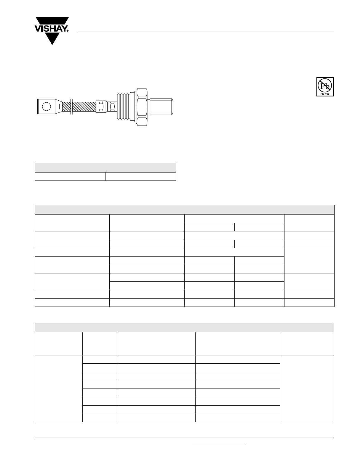
PRODUCT SUMMARY
I
F(AV)
Vishay High Power Products
Standard Recovery Diodes
(Stud Version), 600 A
FEATURES
• Wide current range
• High voltage ratings up to 3200 V
• High surge current capabilities
• Stud cathode and stud anode version
• Standard JEDEC types
• Compression bonded encapsulations
•RoHS complaint
• Lead (Pb)-free
• Designed and qualified for industrial level
TYPICAL APPLICATIONS
• Converters
600 A
• Power supplies
• Machine tool controls
• High power drives
• Medium traction applications
SD600N/R Series
RoHS
COMPLIANT
MAJOR RATINGS AND CHARACTERISTICS
PARAMETER TEST CONDITIONS
I
F(AV)
I
F(RMS)
I
FSM
2
t
I
V
RRM
T
J
T
C
50 Hz 13 000 10 500
60 Hz 13 600 11 000
50 Hz 845 551
60 Hz 772 503
Range 400 to 2000 2200 to 3200 V
ELECTRICAL SPECIFICATIONS
VOLTAGE RATINGS
, MAXIMUM REPETITIVE
V
TYPE NUMBER
SD600N/R
VOLTAGE
CODE
04 400 500
08 800 900
12 1200 1300
16 1600 1700
20 2000 2100
22 2200 2300
28 2800 2900
32 3200 3300
RRM
PEAK REVERSE VOLTAGE
V
SD600N/R
04 to 20 22 to 32
600 A
92 54 °C
940
- 40 to 180 - 40 to 150 °C
V
, MAXIMUM NON-REPETITIVE
RSM
PEAK REVERSE VOLTAGE
V
AT T
UNITS
kA2s
I
MAXIMUM
RRM
= TJ MAXIMUM
J
mA
35
A
Document Number: 93551 For technical questions, contact: ind-modules@vishay.com
Revision: 17-Apr-08 1
www.vishay.com
Page 3
SD600N/R Series
Vishay High Power Products
Standard Recovery Diodes
(Stud Version), 600 A
FORWARD CONDUCTION
PARAMETER SYMBOL TEST CONDITIONS
Maximum average forward current
at case temperature
Maximum RMS forward current I
Maximum peak, one-cycle forward,
non-repetitive surge current
2
Maximum I
Maximum I
t for fusing I2t
2
√t for fusing I2√t t = 0.1 to 10 ms, no voltage reapplied 8450 5510 kA2√s
Low level value of threshold voltage V
High level value of threshold voltage V
Low level value of forward
slope resistance
High level value of forward
slope resistance
Maximum forward voltage drop V
I
F(AV)
F(RMS)
I
FSM
F(TO)1
F(TO)2
r
f1
r
f2
FM
180° conduction, half sine wave
DC at TC = 75 °C (04 to 20), TC = 36 °C (25 to 32) 940
t = 10 ms
t = 8.3 ms 13 600 11 000
t = 10 ms
t = 8.3 ms 11 450 9250
t = 10 ms
t = 8.3 ms 772 503
t = 10 ms
t = 8.3 ms 546 356
(16.7 % x π x I
T
= TJ maximum
J
(I > π x I
(16.7 % x π x I
= TJ maximum
T
J
(I > π x I
No voltage
reapplied
100 % V
RRM
reapplied
No voltage
Sinusoidal half wave,
initial T
reapplied
100 % V
RRM
reapplied
< I < π x I
F(AV)
), TJ = TJ maximum 0.87 0.88
F(AV)
< I < π x I
F(AV)
), TJ = TJ maximum 0.31 0.38
F(AV)
Ipk = 1500 A, TJ = TJ maximum,
t
= 10 ms sinusoidal wave
p
F(AV)
F(AV)
J
),
),
= TJ maximum
SD600N/R
04 to 20 22 to 32
600 A
92 54 °C
570 375 A
100 °C
13 000 10 500
10 900 8830
845 551
598 390
0.78 0.84
0.35 0.40
1.31 1.44 V
UNITS
A
kA2s
V
mΩ
THERMAL AND MECHANICAL SPECIFICATIONS
PARAMETER SYMBOL TEST CONDITIONS
Maximum junction operating
temperature range
Maximum storage temperature range T
Maximum thermal resistance,
junction to case
Maximum thermal resistance,
case to heatsink
Maximum allowed
mounting torque ± 10 %
R
R
T
J
Stg
thJC
thCS
DC operation 0.1
Mounting surface, smooth, flat and greased 0.04
Not-lubricated threads 50 Nm
Approximate weight 454 g
Case style See dimensions (link at the end of datasheet) B-8
www.vishay.com For technical questions, contact: ind-modules@vishay.com
2 Revision: 17-Apr-08
SD600N/R
04 to 20 22 to 32
- 40 to 180 - 40 to 150
- 55 to 200
Document Number: 93551
UNITS
°C
K/W
Page 4

SD600N/R Series
Standard Recovery Diodes
Vishay High Power Products
(Stud Version), 600 A
ΔR
Note
• The table above shows the increment of thermal resistance R
CONDUCTION
thJC
CONDUCTION ANGLE SINUSOIDAL CONDUCTION RECTANGULAR CONDUCTION TEST CONDITIONS UNITS
180°
120°
90°
60°
30°
180
170
160
150
140
130
120
110
100
90
80
Maximum Allowable Case Temperature (°C)
0 100 200 300 400 500 600 700
SD600N/ R Series (400V t o 2000V)
R (DC ) = 0.1 K/ W
thJC
30°
60°
Average Forward Current (A)
Fig. 1 - Current Ratings Characteristics
0.012 0.008
0.014 0.014
0.017 0.019
0.025 0.026
0.042 0.042
when devices operate at different conduction angles than DC
thJC
Conduction Angle
90°
120°
180°
T
= TJ maximum K/W
J
150
140
130
120
110
100
90
80
70
60
50
Maximum Allowable Case Temperature (°C)
SD600N/ R Se ries (2500V to 3200V)
0 100 200 300 400 500 600 700
Average Forward Current (A)
R (DC) = 0.1 K/W
thJC
Cond uction Angle
30°
60°
90°
120°
Fig. 3 - Current Ratings Characteristics
180°
180
170
160
150
140
130
120
110
100
90
80
70
Maximum Allowable Case Temperature (°C)
0 200 400 600 800 1000
SD600N/ R Series (400V t o 2000V)
R (DC) = 0.1 K/W
thJC
Conduction Period
30°
60°
90°
120°
180°
Average Forward Current (A)
Fig. 2 - Current Ratings Characteristics
DC
150
140
130
120
110
100
90
80
70
60
50
40
30
Maximum Allowable Case Temperature (°C)
SD 60 0 N / R Se r i e s ( 2 50 0V t o 32 0 0 V )
30°
0 200 400 600 800 1000
Average Forward Current (A)
R (DC) = 0.1 K/W
thJC
Cond uc tion Period
60°
90°
120°
180°
Fig. 4 - Current Ratings Characteristics
DC
Document Number: 93551 For technical questions, contact: ind-modules@vishay.com
www.vishay.com
Revision: 17-Apr-08 3
Page 5

SD600N/R Series
Vishay High Power Products
800
700
600
500
400
300
200
100
0
Maximum Average Forward Pow er Loss (W)
1100
1000
900
800
700
600
500
400
300
200
100
0
Maximum Average Forward Power Loss (W)
0 200 400 600 800 1000
180°
120°
90°
60°
30°
0 100 200 300 400 500 600
Average Forward Current (A)
DC
180°
120°
90°
60°
30°
RM S Li m i t
Average Forward Current (A)
Standard Recovery Diodes
(Stud Version), 600 A
R
t
0
h
.
S
0
A
4
0
K
.
0
8
K
/
0
.
1
K
/
W
RM S Li m it
Conduction Angle
SD600N/ R Serie s
(400V t o 2000V)
T = 180°C
J
0
.
2
K
/
W
0
.
4
K
/
W
0
.
6
K
/
W
1
K
/
W
1
.
8
K
/
W
20 40 60 80 1 00 120 140 160 180
Maximum Allowable Ambient Temperature (°C)
Fig. 5 - Forward Power Loss Characteristics
R
t
h
S
A
=
0
.
0
4
K
/
W
0
.
0
8
K
/
W
0
.
1K
/
W
0
.
2
K
/
Conduction Period
SD600N/ R Series
(400V t o 2000V)
T = 180°C
J
W
0
.
4
K
/
W
0
.
6
K
/
W
1
K
/
W
1
.
8
K
/
W
20 40 60 80 100 120 140 160 180
Maximum Allowable Ambient Temperature (°C)
Fig. 6 - Forward Power Loss Characteristics
=
/
W
0
.
0
W
0
.
0
2K
2
K
/
W
-
/
W
D
e
l
t
a
R
D
e
l
t
a
R
900
800
700
600
500
400
300
200
100
0
Maximum Average Forward Power Loss (W)
0 100 200 300 400 500 600
180°
120°
90°
60°
30°
RM S Li m i t
Conduction Angle
SD600N/ R Serie s
(2500V t o 3200V)
T = 150°C
J
Average Forward Current (A)
R
t
h
S
A
=
0
0
.
.
0
0
4
2
K
K
/
/
W
0
.
06
0
.
0
0
.
1
W
-
K
1
K
.
2
K
4
K
K
/
W
D
/
W
/
W
/
/
e
l
t
a
R
W
W
25 50 75 100 125 150
Maximum Allowable Ambient Temperature (°C)
Fig. 7 - Forward Power Loss Characteristics
www.vishay.com For technical questions, contact: ind-modules@vishay.com
Document Number: 93551
4 Revision: 17-Apr-08
Page 6

SD600N/R Series
12000
10000
8000
6000
Standard Recovery Diodes
(Stud Version), 600 A
1100
1000
900
800
700
600
500
400
300
200
100
Maximum Average Forward Power Loss (W)
At Any Rated Load Condition And With
Rated V Applied Following Surge.
DC
180°
120°
90°
60°
30°
RM S Li m i t
Cond uction Period
SD600N/ R Serie s
(2500V t o 3200V)
T = 150°C
0
0 100 200 300 400 500 600 700 800 900
Average Forward Current (A)
Fig. 8 - Forward Power Loss Characteristics
RRM
Initial T = 180°C
J
@ 60 Hz 0.0083 s
@ 50 Hz 0.0100 s
Vishay High Power Products
R
t
h
S
A
=
0
0
.
.
0
0
2
4
K
K
/
/
W
0
.
0
0
.
1
0
.
2
0
.
4
1
J
K
25 50 75 100 125 150
Maximum Allowable Ambient Temperature (°C)
W
6
K
K
K
/
-
K
/
/
/
W
D
/
W
W
W
W
e
l
t
a
10000
8000
R
At Any Rated Loa d Cond ition And With
Rated V Applied Following Surge.
RRM
Initial T = 150°C
J
@ 60 Hz 0.0083 s
@ 50 Hz 0.0100 s
6000
4000
SD600N/ R Series
(400V t o 2000V)
Peak Half Sine Wave Forward Current (A)
2000
110100
Number Of Eq ual Amp litud e Ha lf Cyc le Current Pulses (N)
Fig. 9 - Maximum Non-Repetitive Surge Current
14000
Maximum Non Repetitive Surge Current
Versus Pulse Train Durat ion.
12000
Initia l T = 180 °C
J
No Voltage Reapplied
Rated V Reapplied
10000
RRM
8000
6000
4000
SD 6 0 0 N / R Se r i e s
(400V t o 2000V)
Pe ak Ha lf Sin e Wa ve Fo rw a r d Cu rre n t ( A)
2000
0.01 0.1 1
Pulse Train Duration (s)
Fig. 10 - Maximum Non-Repetitive Surge Current
4000
SD 6 0 0N / R Se r i e s
(2500V t o 3200V)
Peak Half Sine Wave Forward Current (A)
2000
110100
Numb er Of Eq ual Amplitude Half Cycle Current Pulses (N)
Fig. 11 - Maximum Non-Repetitive Surge Current
12000
Maxim um Non Re pe titiv e Surg e Curre n t
Versus Pulse Train Duration.
Init ia l T = 150 °C
10000
No Voltage Reapplied
Rated V Reapplied
J
RRM
8000
6000
4000
SD 6 0 0 N / R Se r i e s
(2500V t o 3200V)
Peak Half Sine Wave Forward Current (A)
2000
0.01 0.1 1
Pulse Train Duration (s)
Fig. 12 - Maximum Non-Repetitive Surge Current
Document Number: 93551 For technical questions, contact: ind-modules@vishay.com
www.vishay.com
Revision: 17-Apr-08 5
Page 7

SD600N/R Series
Vishay High Power Products
10000
T = 2 5 ° C
J
T = 18 0° C
1000
SD 6 00 N / R Se r i e s
(400V t o 2000V)
Instantaneous Forward Current (A)
100
01234
Instantaneous Forward Voltage (V)
Fig. 13 - Forward Voltage Drop Characteristics Fig. 14 - Forward Voltage Drop Characteristics
1
thJC
St e a d y St a t e V a l ue :
R = 0.1 K/ W
0.1
(DC Operation)
thJC
Standard Recovery Diodes
(Stud Version), 600 A
J
10000
T = 25 °C
J
T = 150°C
J
1000
SD 6 0 0N / R Se r i e s
(2500V t o 3200V)
Instantaneous Forward Current (A)
100
012345
Instantaneous Forward Voltage (V)
0.01
SD 60 0N / R Se r i e s
Transient Thermal Impedance Z (K/W)
0.001
0.001 0.01 0.1 1 10
Square Wa ve Pulse Dura t ion ( s)
Fig. 15 - Thermal Impedance Z
Characteristics
thJC
www.vishay.com For technical questions, contact: ind-modules@vishay.com
6 Revision: 17-Apr-08
Document Number: 93551
Page 8

SD600N/R Series
Standard Recovery Diodes
ORDERING INFORMATION TABLE
Device code
SD 60 0 N 32 P C
1 - Diode
2 - Essential part number
3 - 0 = Standard recovery
4 - N = Stud normal polarity (cathode to stud)
5 - Voltage code x 100 = V
6 - P = Stud base B-8 3/4" 16UNF-2A
- C = Ceramic cap
7
For metric device M24 x 1.5 contact factory
Vishay High Power Products
(Stud Version), 600 A
51324
R = Stud reverse polarity (anode to stud)
RRM
67
(see Voltage Ratings table)
LINKS TO RELATED DOCUMENTS
Dimensions http://www.vishay.com/doc?95303
Document Number: 93551 For technical questions, contact: ind-modules@vishay.com
Revision: 17-Apr-08 7
www.vishay.com
Page 9

DIMENSIONS in millimeters (inches)
Outline Dimensions
Vishay High Power Products
B-8
Ceramic housing
245 (9.645)
255 (10.04)
115 (4.52) MIN.
27.5 (1.08)
MAX.
12 (0.47) MIN.
38 (1.5)
DIA. MAX.
26 (1.023) MAX.
10.5 (0.41) DIA.
C.S. 70 mm
47 (1.85)
MAX.
21 (0.83) MAX.
5 (0.20) ± 0.3 (0.01)
2
80 (3.15)
MAX.
SW 45
3/4"-16UNF-2A *
*For metric device: M24 x 1.5 - length 21 (0.83) MAX.
contact factory
Document Number: 95303 For technical questions concerning discrete products, contact: diodes-tech@vishay.com
Revision: 11-Apr-08 For technical questions concerning module products, contact: ind-modules@vishay.com
www.vishay.com
1
 Loading...