

6121 Baker Road,
Suite 108
Minnetonka, MN 55345
www.chtechnology.com
Phone (952) 933-6190
Fax (952) 933-6223
1-800-274-4284
Thank you for downloading this document from C&H Technology, Inc.
Please contact the C&H Technology team for the following questions -
Technical ● Application ● Assembly ● Availability ● Pricing
Phone – 1-800-274-4284
E-Mail – sales@chtechnology.com
www.chtechnology.com - SPECIALISTS IN POWER ELECTRONIC COMPONENTS AND ASSEMBLIES
-
www.chtechnology.com
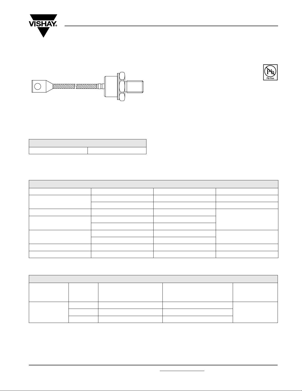
DO-205AB (DO-9)
PRODUCT SUMMARY
I
F(AV)
Vishay High Power Products
Standard Recovery Diodes
(Stud Version), 400 A
FEATURES
• Wide current range
• High voltage ratings up to 2400 V
• High surge current capabilities
• Stud cathode and stud anode version
• Standard JEDEC types
• Compression bonded encapsulations
• Lead (Pb)-free
• Designed and qualified for industrial level
TYPICAL APPLICATIONS
• Converters
400 A
• Power supplies
• Machine tool controls
• High power drives
• Medium traction applications
SD400N/R Series
RoHS
COMPLIANT
MAJOR RATINGS AND CHARACTERISTICS
PARAMETER TEST CONDITIONS VALUES UNITS
I
F(AV)
I
F(RMS)
I
FSM
2
t
I
V
RRM
T
J
T
C
50 Hz 8250
60 Hz 8640
50 Hz 340
60 Hz 311
Range 1600 to 2400 V
480 A
120 °C
630
- 40 to 190 °C
ELECTRICAL SPECIFICATIONS
VOLTAGE RATINGS
TYPE NUMBER
SD400N/R
, MAXIMUM REPETITIVE
V
VOLTAGE
CODE
16 1600 1700
24 2400 2500
RRM
PEAK REVERSE VOLTAGE
V
V
, MAXIMUM NON-REPETITIVE
RSM
PEAK REVERSE VOLTAGE
V
I
AT T
A
kA2s
MAXIMUM
RRM
= TJ MAXIMUM
J
mA
1520 2000 2100
Document Number: 93548 For technical questions, contact: ind-modules@vishay.com
Revision: 17-Apr-08 1
www.vishay.com
SD400N/R Series
Vishay High Power Products
Standard Recovery Diodes
(Stud Version), 400 A
FORWARD CONDUCTION
PARAMETER SYMBOL TEST CONDITIONS VALUES UNITS
400 A
Maximum average forward current
at case temperature
Maximum RMS forward current I
Maximum peak, one-cycle forward,
non-repetitive surge current
2
Maximum I
Maximum I
t for fusing I2t
2
√t for fusing I2√t t = 0.1 to 10 ms, no voltage reapplied 3400 kA2√s
Low level value of threshold voltage V
High level value of threshold voltage V
Low level value of forward
slope resistance
High level value of forward
slope resistance
Maximum forward voltage drop V
I
F(AV)
F(RMS)
I
FSM
F(TO)1
F(TO)2
r
f1
r
f2
FM
180° conduction, half sine wave
DC at 110 °C case temperature 630
t = 10 ms
t = 8.3 ms 8640
t = 10 ms
t = 8.3 ms 7270
t = 10 ms
t = 8.3 ms 311
t = 10 ms
t = 8.3 ms 220
(16.7 % x π x I
T
= TJ maximum
J
(I > π x I
(16.7 % x π x I
T
= TJ maximum
J
(I > π x I
No voltage
reapplied
100 % V
RRM
reapplied
No voltage
Sinusoidal half wave,
= TJ maximum
initial T
J
reapplied
100 % V
RRM
reapplied
< I < π x I
F(AV)
), TJ = TJ maximum 0.85
F(AV)
< I < π x I
F(AV)
), TJ = TJ maximum 0.51
F(AV)
F(AV)
F(AV)
),
),
Ipk = 1500 A, TJ = TJ maximum,
t
= 10 ms sinusoidal wave
p
120 °C
480 A
100 °C
8250
6940
340
241
0.80
0.55
1.62 V
kA
mΩ
A
2
s
V
THERMAL AND MECHANICAL SPECIFICATIONS
PARAMETER SYMBOL TEST CONDITIONS VALUES UNITS
Maximum junction operating
temperature range
Maximum storage temperature range T
Maximum thermal resistance,
junction to case
Maximum thermal resistance,
case to heatsink
Maximum allowed
mounting torque ± 10 %
Approximate weight 250 g
Case style See dimensions (link at the end of datasheet) DO-205AB (DO-9)
www.vishay.com For technical questions, contact: ind-modules@vishay.com
2 Revision: 17-Apr-08
R
R
T
J
Stg
thJC
thCS
- 40 to 190
°C
- 55 to 200
DC operation 0.11
K/W
Mounting surface, smooth, flat and greased 0.04
Not-lubricated threads 27 Nm
Document Number: 93548

SD400N/R Series
Standard Recovery Diodes
Vishay High Power Products
(Stud Version), 400 A
ΔR
Note
• The table above shows the increment of thermal resistance R
CONDUCTION
thJC
CONDUCTION ANGLE SINUSOIDAL CONDUCTION RECTANGULAR CONDUCTION TEST CONDITIONS UNITS
180° 0.020 0.013
120° 0.023 0.023
T
90° 0.029 0.031
= TJ maximum K/W
J
60° 0.042 0.044
30° 0.073 0.074
when devices operate at different conduction angles than DC
thJC
190
180
SD 4 0 0N / R Se r ie s
R (DC) = 0.11 K/W
thJC
170
160
Cond uction Angle
150
140
130
120
110
Maximum Allowable Case Temperature (°C)
0 50 100 150 200 250 300 350 400 450
30°
60°
90°
Average Forward Current (A)
120°
180°
190
180
SD 40 0 N / R Se r i e s
R (DC) = 0.11 K/ W
thJC
170
160
150
Conduction Period
140
130
120
110
100
Maximum Allowable Case Temp erature (°C)
0 100 200 300 400 500 600 700
30°
60°
90°
120°
180°
Average Forward Current (A)
DC
Fig. 1 - Current Ratings Characteristics Fig. 2 - Current Ratings Characteristics
550
0
500
450
400
350
300
250
200
150
100
50
0
Maximum Average Forward Power Loss (W)
180°
120°
90°
60°
30°
Cond uction Angle
SD 40 0N / R Se r i e s
T = 19 0° C
J
0
50 100 150 200 250 300 350 400
Average Forward Current (A)
0
.
3
K
0
.
RM S Li m i t
4
K
/
0
.
6
K
/
1
K
/
W
1
.
8
K
/
10 30 50 70 90 110 130 150 170 190
Maximum Allowable Ambient Temp erature (°C)
.
R
1
K
t
h
0
.
2K
/
W
W
W
W
/
W
S
/
W
A
=
0
.
0
4
K
/
W
D
e
l
t
a
R
Fig. 3 - Forward Power Loss Characteristics
Document Number: 93548 For technical questions, contact: ind-modules@vishay.com
www.vishay.com
Revision: 17-Apr-08 3

SD400N/R Series
Vishay High Power Products
800
700
600
500
400
300
200
100
Maximum Averag e Forward Power Loss ( W)
8000
At Any Rated Load Condition And With
Rated V Applied Following Surge.
7000
RRM
6000
5000
4000
3000
SD 40 0N / R Se r i e s
Peak Half Sine Wave Forward Current (A)
2000
110100
Numb er Of Eq ua l Amp litud e Ha lf Cyc le C urrent Pulses (N)
Fig. 5 - Maximum Non-Repetitive Surge Current Fig. 6 - Maximum Non-Repetitive Surge Current
DC
180°
120°
90°
60°
30°
RM S Li mi t
0
0 100 200 300 400 500 600 700
Average Forward Current (A)
Init ial T = 190°C
J
@ 60 Hz 0.0083 s
@ 50 Hz 0.0100 s
Standard Recovery Diodes
(Stud Version), 400 A
R
t
h
0
.
S
1
A
K
/
=
W
0
.
0
4
K
/
W
Peak Half Sine Wave Forwa rd Current (A)
9000
8000
7000
6000
5000
4000
3000
2000
1000
D
e
0
.
2
K
/
W
0
.
3
K
/
W
0
.
4
K
/
Conduc tion Period
SD 4 0 0N / R Se r i e s
T = 190°C
J
W
0
.
6
K
/
W
1
K
/
W
1
.
8
K
/
W
10 30 50 70 90 110 130 150 170 190
Maximum Allowable Ambient Temperature (°C)
Fig. 4 - Forward Power Loss Characteristics
l
t
a
R
Maximum Non Repetitive Surge Current
Versus Pulse Train Duration.
Init ial T = 190°C
J
No Volt ag e Rea pp lie d
Rated V Reapplied
RRM
SD 4 0 0N / R Se r i e s
0.01 0.1 1
Pulse Tra i n Du ra t io n ( s)
10000
SD 40 0N / R Se r i e s
1000
T = 25 ° C
J
T = 19 0 ° C
J
Instantaneous Forward Current (A)
100
0.5 1 1.5 2 2.5
In st a nt a n e o us Fo rw a rd V olt a g e ( V )
Fig. 7 - Forward Voltage Drop Characteristics
www.vishay.com For technical questions, contact: ind-modules@vishay.com
Document Number: 93548
4 Revision: 17-Apr-08

SD400N/R Series
Standard Recovery Diodes
1
thJC
0.01
Transient Thermal Impeda nce Z (K/W)
0.001
ORDERING INFORMATION TABLE
Device code
St e a d y St a t e V a l u e :
R = 0.11 K/W
0.1
thJC
(DC Operation)
0.001 0.01 0.1 1 10
SD 40 0 N 24 P C
(Stud Version), 400 A
Sq u a r e W a v e Pu l s e D u r a t i o n ( s )
Fig. 8 - Thermal Impedance Z
SD 40 0 N / R Se r i e s
Characteristic
thJC
Vishay High Power Products
51324
67
1 - Diode
2 - Essential part number
3 - 0 = Standard recovery
4 - N = Stud normal polarity (cathode to stud)
R = Stud reverse polarity (anode to stud)
5 - Voltage code x 100 = V
(see Voltage Ratings table)
RRM
6 - P = Stud base DO-205AB (DO-9) 3/4" 16UNF-2A
- C = Ceramic housing
7
For metric device M16 x 1.5 contact factory
LINKS TO RELATED DOCUMENTS
Dimensions http://www.vishay.com/doc?95301
Document Number: 93548 For technical questions, contact: ind-modules@vishay.com
Revision: 17-Apr-08 5
www.vishay.com

DIMENSIONS in millimeters (inches)
Outline Dimensions
Vishay Semiconductors
DO-205AB (DO-9)
Ceramic housing
210 (8.27)
± 10 (0.39)
82 (3.23)
MIN.
DIA. 8.5 (0.33) NOM.
DIA. 27.5
(1.08) MAX.
21 (0.82)
MAX.
9.5 (0.37) MIN.
16 (0.63)
MAX.
19 (0.75)
MAX.
39 (1.53)
MAX.
C.S. 35 mm
(0.054 s.i.)
SW 32
4 (0.16)
MAX.
2
3/4"-16UNF-2A*
Document Number: 95301 For technical questions, contact: indmodules@vishay.com
Revision: 09-Apr-08 1
*For metric device: M16 x 1.5
contact factory
www.vishay.com

Legal Disclaimer Notice
www.vishay.com
Vishay
Disclaimer
ALL PRODUCT, PRODUCT SPECIFICATIONS AND DATA ARE SUBJECT TO CHANGE WITHOUT NOTICE TO IMPROVE
RELIABILITY, FUNCTION OR DESIGN OR OTHERWISE.
Vishay Intertechnology, Inc., its affiliates, agents, and employees, and all persons acting on its or their behalf (collectively,
“Vishay”), disclaim any and all liability for any errors, inaccuracies or incompleteness contained in any datasheet or in any other
disclosure relating to any product.
Vishay makes no warranty, representation or guarantee regarding the suitability of the products for any particular purpose or
the continuing production of any product. To the maximum extent permitted by applicable law, Vishay disclaims (i) any and all
liability arising out of the application or use of any product, (ii) any and all liability, including without limitation special,
consequential or incidental damages, and (iii) any and all implied warranties, including warranties of fitness for particular
purpose, non-infringement and merchantability.
Statements regarding the suitability of products for certain types of applications are based on Vishay’s knowledge of typical
requirements that are often placed on Vishay products in generic applications. Such statements are not binding statements
about the suitability of products for a particular application. It is the customer’s responsibility to validate that a particular
product with the properties described in the product specification is suitable for use in a particular application. Parameters
provided in datasheets and/or specifications may vary in different applications and performance may vary over time. All
operating parameters, including typical parameters, must be validated for each customer application by the customer’s
technical experts. Product specifications do not expand or otherwise modify Vishay’s terms and conditions of purchase,
including but not limited to the warranty expressed therein.
Except as expressly indicated in writing, Vishay products are not designed for use in medical, life-saving, or life-sustaining
applications or for any other application in which the failure of the Vishay product could result in personal injury or death.
Customers using or selling Vishay products not expressly indicated for use in such applications do so at their own risk and agree
to fully indemnify and hold Vishay and its distributors harmless from and against any and all claims, liabilities, expenses and
damages arising or resulting in connection with such use or sale, including attorneys fees, even if such claim alleges that Vishay
or its distributor was negligent regarding the design or manufacture of the part. Please contact authorized Vishay personnel to
obtain written terms and conditions regarding products designed for such applications.
No license, express or implied, by estoppel or otherwise, to any intellectual property rights is granted by this document or by
any conduct of Vishay. Product names and markings noted herein may be trademarks of their respective owners.
Material Category Policy
Vishay Intertechnology, Inc. hereby certifies that all its products that are identified as RoHS-Compliant fulfill the
definitions and restrictions defined under Directive 2011/65/EU of The European Parliament and of the Council
of June 8, 2011 on the restriction of the use of certain hazardous substances in electrical and electronic equipment
(EEE) - recast, unless otherwise specified as non-compliant.
Please note that some Vishay documentation may still make reference to RoHS Directive 2002/95/EC. We confirm that
all the products identified as being compliant to Directive 2002/95/EC conform to Directive 2011/65/EU.
Revision: 12-Mar-12
1
Document Number: 91000
 Loading...