

Page 1

6121 Baker Road,
Suite 108
Minnetonka, MN 55345
www.chtechnology.com
Phone (952) 933-6190
Fax (952) 933-6223
1-800-274-4284
Thank you for downloading this document from C&H Technology, Inc.
Please contact the C&H Technology team for the following questions -
Technical
Application
Assembly
Availability
Pricing
Phone – 1-800-274-4284
E-Mail – sales@chtechnology.com
www.chtechnology.com - SPECIALISTS IN POWER ELECTRONIC COMPONENTS AND ASSEMBLIES - www.chtechnology.com
Page 2
QID4515001
Powerex, Inc., 173 Pavilion Lane, Youngwood, Pennsylvania 15697 (724) 925-7272
www.pwrx.com
A
S NUTS
(3TYP)
EB
G (3TYP)
T (SCREWING
DEPTH)
F F
1
D
8
7
32
4
R (DEEP)
K
(3TYP)
4
5
6
1
2
L
(2TYP)
J (2TYP)
H
6
5
M
H
V (4TYP)
U (5TYP)
P
Q
C
N
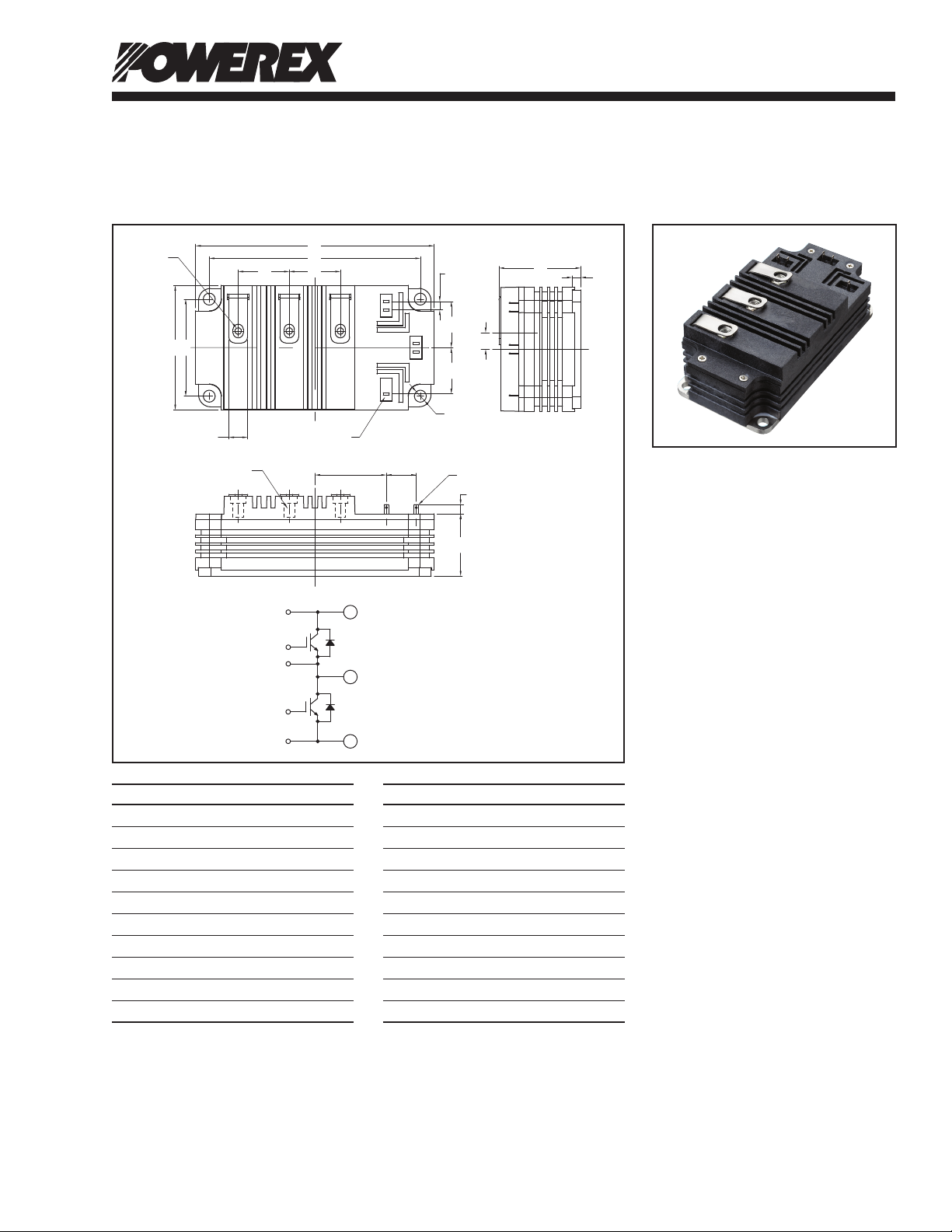
Dual IGBTMOD™
HVIGBT Module
150 Amperes/4500 Volts
Description:
Powerex IGBTMOD™ Modules
are designed for use in switching
applications. Each module consists
of two IGBT Transistors in a
half-bridge configuration with each
transistor having a reverseconnected super-fast recovery
free-wheel diode. All components
and interconnects are isolated
from the heat sinking baseplate,
offering simplified system assembly
and thermal management.
8
7
Outline Drawing and Circuit Diagram
Dimensions Inches Millimeters
A 5.51 140.0
B 2.87 73.0
C 1.89 48.0
D 4.88±0.01 124.0±0.25
E 2.24±0.01 57.0±0.25
F 1.18 30.0
G 0.43 11.0
H 1.07 27.15
J 0.20 5.0
K 1.65 42.0
3
Dimensions Inches Millimeters
L 0.69±0.01 17.5±0.25
M 0.38 9.75
N 0.20 5.0
P 0.22 5.5
Q 1.44 36.5
R 0.16 4.0
S M6 Metric M6
T 0.63 Min. 16.0 Min.
U 0.11 x 0.02 2.8 x 0.5
V 0.28 Dia. 7.0 Dia.
Features:
Low V
CE(sat)
Creepage and Clearance
meet IEC 60077-1
High Isolation Voltage:
10.2KVRMS
Rugged SWSOA and RRSOA
Compact Industry Standard
Package
Applications:
Traction
Medium Voltage Drives
High Voltage Power Supplies
111/11 Rev. 6
Page 3

Powerex, Inc., 173 Pavilion Lane, Youngwood, Pennsylvania 15697 (724) 925-7272 www.pwrx.com
QID4515001
Dual IGBTMOD™ HVIGBT Module
150 Amperes/4500 Volts
Absolute Maximum Ratings, Tj = 25 °C unless otherwise specied
Ratings Symbol QID4515001 Units
Junction Temperature Tj -40 to 150 °C
Storage Temperature T
Collector-Emitter Voltage (VGE = 0V) V
Gate-Emitter Voltage (VCE = 0V) V
Collector Current (TC = 25°C) IC 150 Amperes
Peak Collector Current (Pulse) ICM 300* Amperes
Diode Forward Current** (TC = 25°C) IF 150 Amperes
Diode Forward Surge Current** (Pulse) IFM 300* Amperes
I2t for Diode (t = 10ms) I2t 10 kA2sec
Maximum Collector Dissipation (TC = 25°C, IGBT Part, T
≤ 150°C) PC 1440 Watts
j(max)
Mounting Torque, M6 Terminal Screws — 44 in-lb
Mounting Torque, M6 Mounting Screws — 44 in-lb
Module Weight (Typical) — 900 Grams
Isolation Voltage (Charged Part to Baseplate, AC 60Hz 1 min.) V
Partial Discharge Qpd 10 pC
(V1 = 4800 V
, V2 = 3500 V
RMS
, f = 60Hz (Acc. to IEC 1287))
RMS
Maximum Short-Circuit Pulse Width, t
(VCC ≤ 3200V, VGE = ±15V, R
≥ 60Ω, Tj = 125°C)
G(off)
-40 to 125 °C
stg
4500 Volts
CES
±20 Volts
GES
9.0 kVolts
iso
10 µs
psc
Electrical Characteristics, Tj = 25 °C unless otherwise specied
Characteristics Symbol Test Conditions Min. Typ. Max. Units
Collector-Cutoff Current I
Gate Leakage Current I
Gate-Emitter Threshold Voltage V
Collector-Emitter Saturation Voltage V
IC = 150A, VGE = 15V, Tj = 125°C — 4.0 — Volts
Total Gate Charge QG VCC = 2250V, IC = 150A, VGE = 15V — 1.4 — µC
Emitter-Collector Voltage** VEC IE = 150A, VGE = 0V — 4.7 5.6 Volts
* Pulse width and repetition rate should be such that device junction temperature (Tj) does not exceed T
**Represents characteristics of the anti-parallel, emitter-to-collector free-wheel diode (FWDi).
*** Pulse width and repetition rate should be such that device junction temperature rise is negligible.
VCE = V
CES
VGE = V
GES
IC = 10mA, VCE = 10V 4.5 6.0 7.5 Volts
GE(th)
IC = 150A, VGE = 15V, Tj = 25°C — 3.5 3.9*** Volts
CE(sat)
, VGE = 0V — — 2.7 mA
CES
, VCE = 0V — — 0.5 µA
GES
rating.
j(max)
2 11/11 Rev. 6
Page 4

Powerex, Inc., 173 Pavilion Lane, Youngwood, Pennsylvania 15697 (724) 925-7272 www.pwrx.com
QID4515001
Dual IGBTMOD™ HVIGBT Module
150 Amperes/4500 Volts
Electrical Characteristics, Tj = 25 °C unless otherwise specied
Characteristics Symbol Test Conditions Min. Typ. Max. Units
Input Capacitance C
Output Capacitance C
Reverse Transfer Capacitance C
Resistive Turn-on Delay Time t
Load Rise Time tr VGE = ±15V, — — 0.5 µs
Switching Turn-off Delay Time t
Times Fall Time tf Inductive Load — — 1.2 µs
Turn-on Switching Energy Eon Tj = 125°C, IC = 150A, VGE = ±15V, — 600 — mJ/P
Turn-off Switching Energy E
LS = 180nH , Inductive Load
Diode Reverse Recovery Time** trr VCC = 2250V, IE = 150A, — — 1.8 µs
Diode Reverse Recovery Charge** Qrr VGE = ±15V, R
Diode Reverse Recovery Energy E
Stray Inductance (C1-E2) L
Lead Resistance Terminal-Chip RCE — 0.8 — mΩ
— 18 — nF
ies
VGE = 0V, VCE = 10V — 1.33 — nF
oes
— 0.4 — nF
res
VCC = 2250V, IC = 150A, — — 1.5 µs
d(on)
RG = 60Ω, LS = 180nH — — 3.5 µs
d(off)
RG = 60Ω, VCC = 2250V, — 450 — mJ/P
off
= 60Ω, — 81* — µC
G(on)
LS = 180nH , Inductive Load — 55 — mJ/P
rec
— 60 — nH
SCE
Thermal and Mechanical Characteristics, Tj = 25 °C unless otherwise specied
Characteristics Symbol Test Conditions Min. Typ. Max. Units
Thermal Resistance, Junction to Case*** R
Thermal Resistance, Junction to Case*** R
Contact Thermal Resistance, Case to Fin R
Thermal Grease Applied, λ
Comparative Tracking Index CTI 600 — —
Clearance Distance in Air (Terminal to Base) d
Creepage Distance Along Surface d
(Terminal to Base)
Clearance Distance in Air d
(Terminal to Terminal)
Creepage Distance Along Surface d
(Terminal to Terminal)
*Pulse width and repetition rate should be such that device junction temperature rise is negligible.
**Represents characteristics of the anti-parallel, emitter-to-collector free-wheel diode (FWDi).
***TC measurement point is just under the chips.
Q Per IGBT — 0.082 0.087 °C/W
th(j-c)
D Per FWDi — 0.164 0.174 °C/W
th(j-c)
Per Module, — 0.018 — °C/W
th(c-f)
= 1W/mK
grease
35.0 — — mm
a(t-b)
64 — — mm
s(t-b)
19 — — mm
a(t-t)
54 — — mm
s(t-t)
311/11 Rev. 6
Page 5
Powerex, Inc., 173 Pavilion Lane, Youngwood, Pennsylvania 15697 (724) 925-7272 www.pwrx.com
QID4515001
Dual IGBTMOD™ HVIGBT Module
150 Amperes/4500 Volts
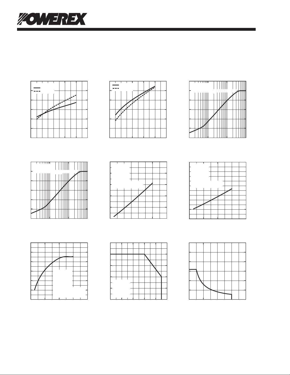
SATURATION VOLTAGE CHARACTERISTICS
6
5
, (VOLTS)
4
CE(sat)
COLLECTOR-EMITTER
VGE = 15V
= 25°C
T
j
= 125°C
T
j
(TYPICAL)
3
2
COLLECTOR-EMITTER
1
SATURATION VOLTAGE, V
0
0 50 100 200
COLLECTOR CURRENT, IC, (AMPERES)
TRANSIENT THERMAL
th(j-c)
1.2
1.0
IMPEDANCE CHARACTERISTICS
Single Pulse
= 25°C
T
C
Per Unit Base = R
(FWDi)
th(j-c)
= 0.174 K/W
0.8
0.6
• (NORMALIZED VALUE)
0.4
th
= R
th
Z
0.2
0
-3
NORMALIZED TRANSIENT THERMAL IMPEDANCE, Z
10
REVERSE RECOVERY CHARACTERISTICS
-2
10
TIME, (s)
10
FREE-WHEEL DIODE
(TYPICAL)
75.0
TRANSIENT THERMAL
IMPEDANCE CHARACTERISTICS
Single Pulse
= 25°C
T
C
Per Unit Base = R
-3
HALF-BRIDGE TURN-OFF SWITCHING
VCC = 2250V
V
GE
= 60
R
G
= 180nH
L
S
= 125°C
T
j
Inductive Load Integrated
Over Range of 10%
(IGBT)
= 0.087 K/W
th(j-c)
-2
10
TIME, (s)
ENERGY CHARACTERISTICS
(TYPICAL)
-1
10
= ±15V
0
10
6
5
, (VOLTS)
EC
4
3
2
1
EMITTER-COLLECTOR VOLTAGE, V
250150
0
1250
, (mJ/P)
1000
on
750
FREE-WHEEL DIODE
FORWARD CHARACTERISTICS
0 50 100 200
HALF-BRIDGE TURN-ON SWITCHING
VCC = 2250V
V
GE
= 60
R
G
= 180nH
L
S
= 125°C
T
j
Inductive Load Integrated
Over Range of 10%
(TYPICAL)
Tj = 25°C
= 125°C
T
j
EMITTER CURRENT, IE, (AMPERES)
ENERGY CHARACTERISTICS
(TYPICAL)
= ±15V
th(j-c)
1.2
1.0
0.8
0.6
• (NORMALIZED VALUE)
0.4
th
= R
th
Z
0.2
0
NORMALIZED TRANSIENT THERMAL IMPEDANCE, Z
250150
10
750
625
, (mJ/P)
off
500
375
500
250
250
TURN-OFF SWITCHING ENERGY, E
-1
0
10
0
0 50 100 150 200
COLLECTOR CURRENT, IC, (AMPERES)
TURN-OFF SWITCHING
SAFE OPERATING AREA (RBSOA)
(TYPICAL)
250
125
TURN-OFF SWITCHING ENERGY, E
0
0 50 100 150 200
COLLECTOR CURRENT, IC, (AMPERES)
DIODE REVERSE RECOVERY
SAFE OPERATING AREA
(TYPICAL)
375
62.5
, (mJ/P)
rec
50.0
37.5
25.0
12.5
REVERSE RECOVERY ENERGY, E
0
0 50 100 150 200
EMITTER CURRENT, I
VCC = 2250V
V
= ±15V
GE
= 60
R
G
= 180nH
L
S
= 25°C
T
j
Inductive Load Integrated
Over Range of 10%
IGBT Drive Conditions
, (AMPERES)
E
200
, (VOLTS)
C
150
100
VCC = 3000V
V
= ±15V
GE
= 60
R
50
COLLECTOR CURRENT, I
G
= 100nH
L
S
= 125°C
T
j
0
0 1000 2000 3000 4000 5000
COLLECTOR-EMITTER VOLTAGE, VCE, (VOLTS)
312
, (AMPERES)
rr
250
187
125
62
REVERSE RECOVERY CURRENT, I
0
0 1000 2000 3000 4000
COLLECTOR-EMITTER VOLTAGE, VCE, (VOLTS)
4 11/11 Rev. 6
 Loading...