

Page 1
PS51787
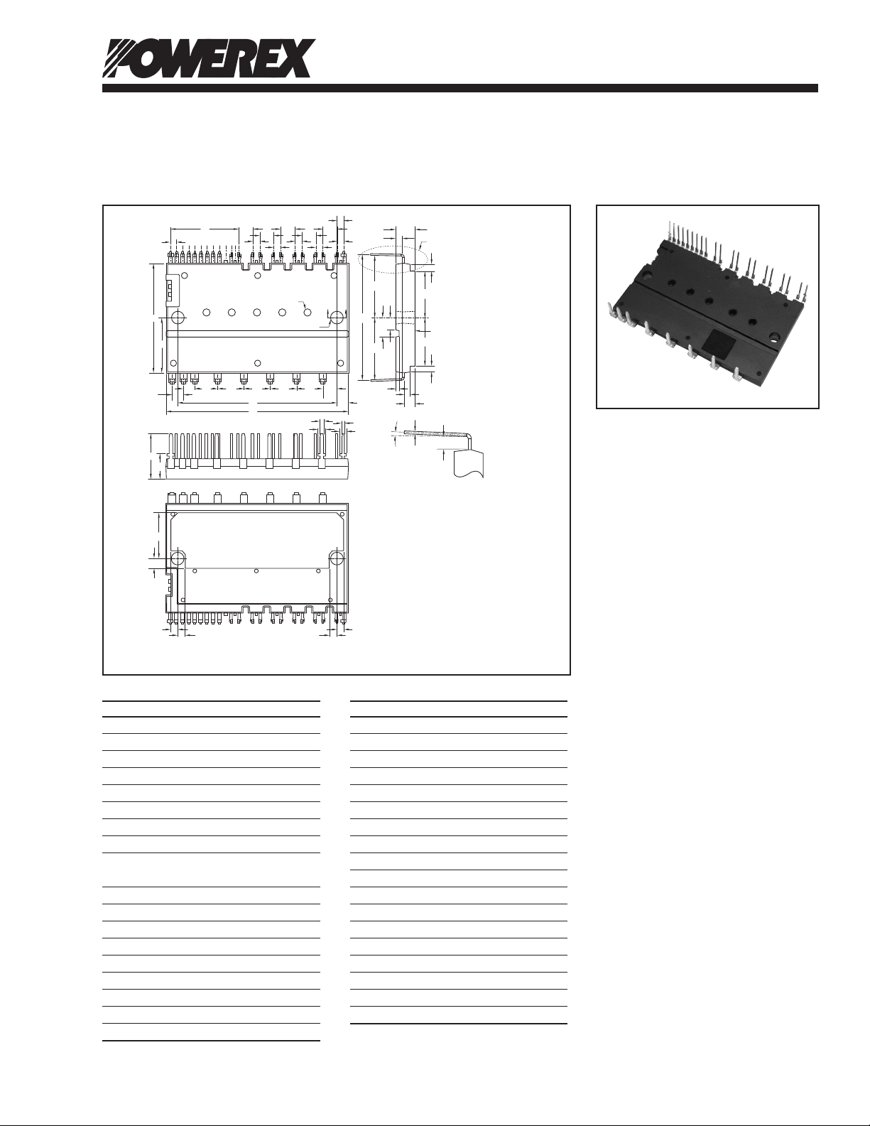
HEATSINK
SIDE
E F
F F
F F
L
M
T
S
U
V
W
Y
X
AG
AM
AL
N
P
P
R
Q
D
B
H
Z
Z
AE
AF
W
L
C
AG
V
TT
AJ
AK
AHAH
ACAB ABAB AB
AA
AD
A
D
D
D
D
D
G
K
J
20 VIN
21 VIN
22 GND
23 VD
24 VD
25 RG
26 RG
27 RG
28 RG
29 (VND)
30 (N2)
31 N
32 N
33 N
34 N
35 R
36 S
37 S
38 P
1 N
2
2 (N2)
3 N2
4 N2
5 (N2)
6 N2
7 N2
8 (N2)
9 N
2
10 N2
11 (N2)
12 N2
13 VND
14 (VNO)
15 VND
16 SG
17 (SG)
18 SG
19 (GND)
TERMINAL
CODE
DETAIL "A"
DETAIL "A"
1
1819202122232425262728
1234
567891011121314151617
3837363534333231
29
30
NOTE: Do not connect RG and SG terminal to any wire on the PCB.
Powerex, Inc., 173 Pavilion Lane, Youngwood, Pennsylvania 15697 (724) 925-7272
www.pwrx.com
Intellimod™ Module
Dual-In-Line Intelligent
Power Factor Correction Module
20 Amperes/600 Volts
Description:
DIPPFC™ is an intelligent power
factor correction module that
integrates power devices, drivers
and protection circuitry in an ultracompact dual-in-line package.
Design time is reduced by the
use of application-specific HVIC
and a bridge-less topology.
Overall efficiency and reliability
are increased by use of CSTBT
technology and low thermal
impedance.
Features:
Outline Drawing and Circuit Diagram
Dimensions Inches Millimeters
A 2.07 52.5
B 1.22 31.0
C 1.81±0.008 46.0±0.2
D 0.07±0.008 1.78±0.2
E 0.77 19.58
F 0.17±0.008 4.32±0.2
G 0.08±0.019 2.04±0.3
H 0.61 15.5
J 0.09 Dia. x 2.2 Dia. x
0.1 Depth 2.6 Depth
K 0.13 Dia. 3.3 Dia.
L 0.08 2.0
M 0.22 5.6
N 1.41±0.02 35.9±0.5
P 0.69 17.7
Q 0.216 5.5
R 0.14 3.5
S 0.503 12.78
T 0.09 2.2
Dimensions Inches Millimeters
U 0.53 13.5
V 0.06 1.5
W 0.04 1.0
X 0.12 3.1±0.1
Y 0.06 1.55
Z 0.13±0.019 3.3±0.3
AA 0.26±0.019 6.6±0.3
AB 0.3±0.019 7.62±0.3
AC 0.15±0.019 3.95±0.3
AD 0.13 3.25
AE 0.5 12.7
AF 0.28 7.1
AG 0.02 0.5
AH 0.067 1.7
AJ 0.11 2.8
AK 0.51 13.0
AL 0° ~ 5°
AM 0.078 1.96
Low-loss CSTBT IGBTs
Single Power Supply
Efficient bridge-less Topology
Integrated HVIC
Applications:
HVAC
Compressors
Pumps
Ordering Information:
PS51787 is a 600V, 20 A
RMS
DIPPFC™ Module.
103/10 Rev. 0
Page 2
Powerex, Inc., 173 Pavilion Lane, Youngwood, Pennsylvania 15697 (724) 925-7272 www.pwrx.com
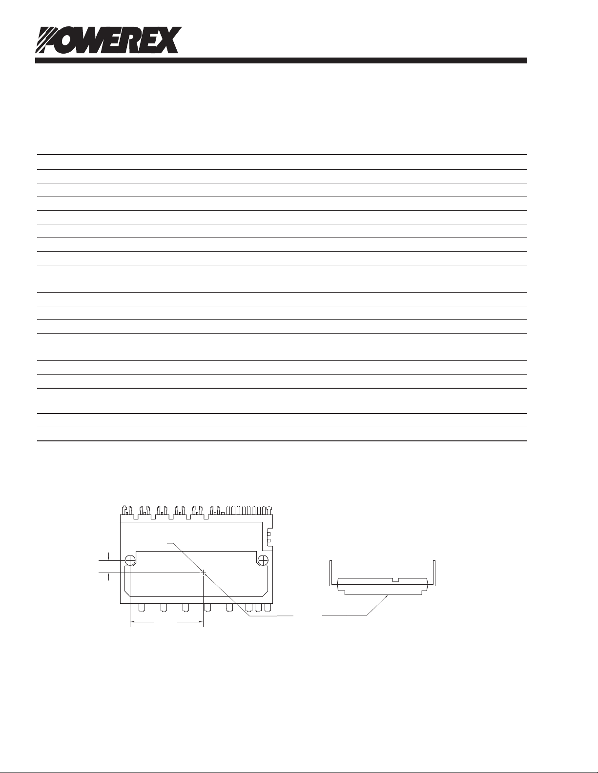
4.6 mm
25.4mm
IGBT
CONTROL TERMINALS
POWER TERMINALS
TC POINT
PS51787
Intellimod™ Module
Dual-In-Line Intelligent Power Factor Correction Module
20 Amperes/600 Volts
Absolute Maximum Ratings, Tj = 25°C unless otherwise specified
Characteristics Symbol PS51787 Units
Input Supply Voltage (Between S-R Terminals) Vi 264 V
Input Supply Voltage, Surge (Between S-R Terminals) V
500 Volts
i(surge)
Output Voltage (Between P-N Terminals) VO 450 Volts
Output Voltage, Surge (Between P-N Terminals) V
Collector-Emitter Voltage V
Repetative Peak Reverse Voltage V
Input Current, 100% Load (TC ≤ 100°C, Vi = 220V
Input Current, 125% Load (TC ≤ 100°C, Vi = 220V
f
= 20kHz, Non-repetative, within 1 Minute)
PWM
, VO = 390V, f
rms
, VO = 390V, I
rms
= 20kHz) Ii 20 A
PWM
500 Volts
O(surge)
600 Volts
CES
600 Volts
RRM
25 A
i(125%)
I2t for Fusing (Value for 1 Cycle of Surge Current, tw = 8.3ms, Non-repetitive) I2t 120 A2s
Junction Temperature* Tj -20 to 150 °C
Module Case Operation Temperature** TC -20 to 100 °C
Storage Temperature T
-40 to 125 °C
stg
Mounting Torque, M3 Mounting Screws — 8.7 in-lb
Module Weight (Typical) — 21 Grams
Isolation Voltage, AC 1 minute, 60Hz Sinusoidal, Connection Pins to Heatsink Plate V
2500 Vrms
ISO
rms
rms
rms
Control Sector
Control Supply Voltage (Applied between VD-GND) VD 20 Volts
Input Voltage (Applied between VIN-GND) VIN 0 ~ VD+0.5 Volts
*The maximum junction temperature rating of the power chips integrated within the DIPPFC is 150°C (@TC ≤ 100°C). However, to ensure safe operation of the DIPPFC,
the average junction temperature should be limited to T
≤ 125°C (@TC ≤ 100°C).
j(avg)
**TC Measurement Point
2 03/10 Rev. 0
Page 3

Powerex, Inc., 173 Pavilion Lane, Youngwood, Pennsylvania 15697 (724) 925-7272 www.pwrx.com
PS51787
Intellimod™ Module
Dual-In-Line Intelligent Power Factor Correction Module
20 Amperes/600 Volts
Electrical and Mechanical Characteristics, Tj = 25°C unless otherwise specified
Characteristics Symbol Test Conditions Min. Typ. Max. Units
Collector-Emitter Saturation Voltage V
H-Diode Forward Voltage* V
L-Diode Forward Voltage* V
Switching Times ton — 0.25 0.35 µs
t
t
t
t
Collector-Emitter Cutoff Current I
V
Reverse Current IR V
V
Diode Recovery Current Irr V
V
CE(sat)
I
F(H)
I
F(L)
V
C(on)
I
off
Inductive Load, VIN = 0 ⇔ 5V — 0.18 0.35 µs
C(off)
rr
V
CES
= 15V, VIN = 5V, IC = 30A — 1.9 2.5 Volts
D
= 30A, Applied Between R-P, S-P — 1.9 2.5 Volts
F
= 30A, Applied Between N2-R, N2-S — 1.0 1.3 Volts
F
= 300V, VD = 15V, — 0.14 0.23 µs
CC
= 30A, Tj = 125°C, — 0.40 0.65 µs
C
— 0.11 — µs
= 600V, Tj = 25°C — — 1.0 mA
CE
= 600V, Tj = 125°C — — 10 mA
CE
= 600V, Tj = 25°C — — 1.0 mA
R
= 600V, Tj = 125°C — — 10 mA
R
= 300V, VD = 15V, IC = 30A — 11 — Amperes
CC
Control Sector
Circuit Current I
D
V
Applied Between VD-GND, — 0.7 3.0 mA
V
Input Current IIN V
ON Threshold Voltage V
OFF Threshold Voltage V
Applied Between VIN-GND — 2.1 2.6 Volts
th(on)
Applied Between VIN-GND 0.8 1.3 — Volts
th(off)
Supply Circuit Undervoltage UVDt Trip Level, Tj ≤ 125°C 10.3 — 12.5 Volts
Protection UVDr Reset Level, Tj ≤ 125°C 10.8 — 13.0 Volts
Applied Between VD-GND, — 0.8 3.0 mA
= 15V, VIN = 5V
D
= 15V, VIN = 0V
D
= 15V, VIN = 5V — 0.3 0.45 mA
D
Thermal Characteristics, Tj = 25°C unless otherwise specified
Characteristic Symbol Condition Min. Typ. Max. Units
Thermal Resistance Junction to Case R
Thermal Resistance Junction to Case R
IGBT Part (Per 1 Chip) — — 0.96 °C/Watt
th(j-C)Q
FWDi Part (Per 1 Chip) — — 1.35 °C/Watt
th(j-C)D
Recommended Conditions for Use
Characteristic Symbol Condition Min. Typ. Max. Units
Input Supply Voltage Vi Applied between S-R 90 — 264 V
Control Supply Voltage VD Applied between VD-GND 13.5 15.0 16.5 Volts
Control Supply Variation
PWM Input Frequency f
*H-Diode and L-Diode corresponds to Diode1, Diode 2 and Diode 3, Diode 4 in the Application circuit.
∆VD -1 — 1 V/µs
T
PWM
≤ 100°C, Tj ≤ 125°C — 20 — kHz
C
rms
303/10 Rev. 0
Page 4

Powerex, Inc., 173 Pavilion Lane, Youngwood, Pennsylvania 15697 (724) 925-7272 www.pwrx.com
V
CC
CONTROL IC
R
OUT
RG
V
D
V
IN
V
NO
GND
SG
MCU
S
OUT
V
NO
V
IN
A
B
N2
N
C2
C1
+
S
R
P
GND
IGBT1
FWDi4 FWDi3
FWDi2 FWDi1
IGBT2
C4
C3
15V
LINE
NOTE:
1. Due to high speed and large surge voltage switching, the area P-C1-N should be a small as possible. (C1: good temperature,
frequency characteristic electrolytic type). Also add a bypass condenser (C2) with good frequency response such as polypropylene
as close as possible to the P and N terminals.
2. To prevent erroneous protection, the wiring of A, B should be as short as possible.
3. It is recommended to insert a high-speed clamp diode between V
NO
-GND terminals to prevent surge destruction.
4. C3 and C4 capacitors should be mounted as close to the terminals of the DIPPFC as possible. C3, good temperature, frequency
characteristic electrolytic type and C4, good temperature, frequency and DC bias characteristic ceramic type are recommended.
5. It is recommended to insert a Zener diode (24V/1W) between each pair of control supply terminals to prevent surge destruction.
6. Please connect adjacent terminals with the same name together on the PCB. (N, N2, V
NO
, VIN, VD, S)
7. Do not connect RG and SG terminals to any wire on the PCB.
PS51787
Intellimod™ Module
Dual-In-Line Intelligent Power Factor Correction Module
20 Amperes/600 Volts
Application Circuit
4 03/10 Rev. 0
 Loading...