

Page 1

6121 Baker Road,
Suite 108
Minnetonka, MN 55345
www.chtechnology.com
Phone (952) 933-6190
Fax (952) 933-6223
1-800-274-4284
Thank you for downloading this document from C&H Technology, Inc.
Please contact the C&H Technology team for the following questions -
Technical
Application
Assembly
Availability
Pricing
Phone – 1-800-274-4284
E-Mail – sales@chtechnology.com
www.chtechnology.com - SPECIALISTS IN POWER ELECTRONIC COMPONENTS AND ASSEMBLIES - www.chtechnology.com
Page 2
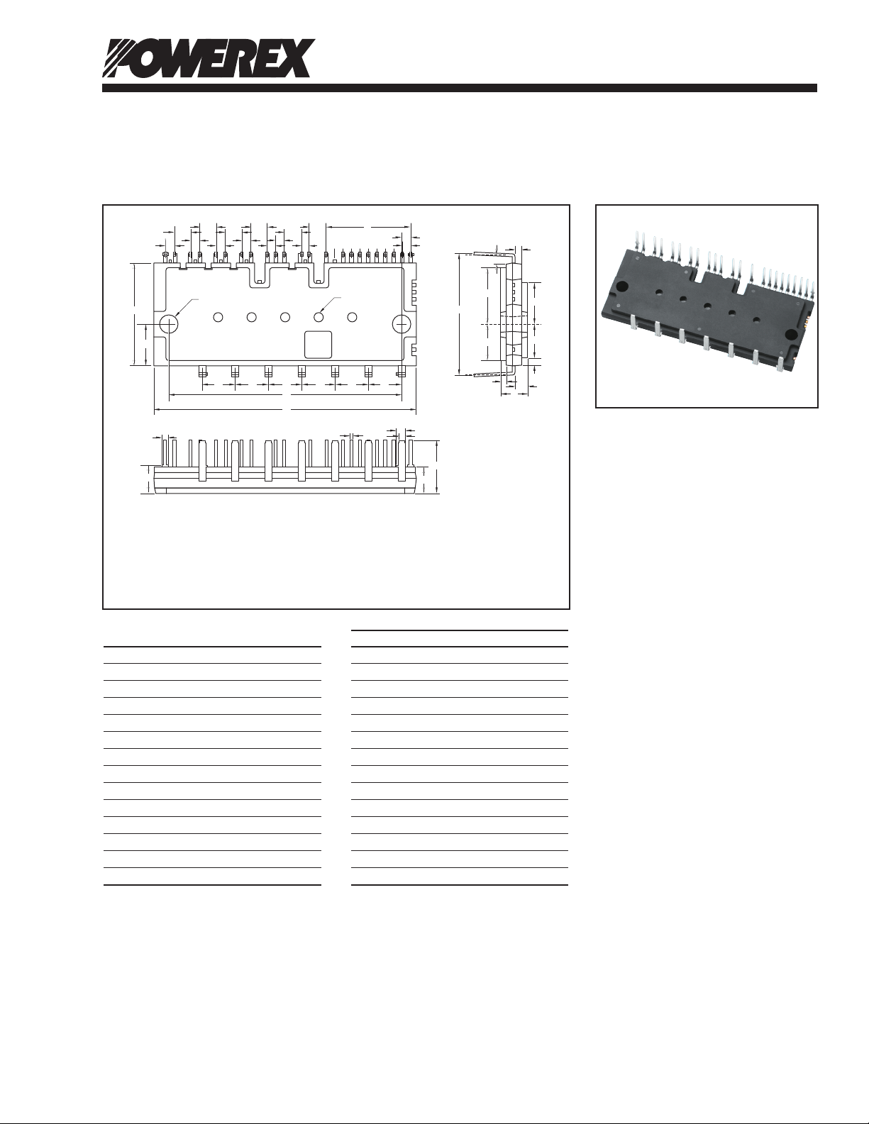
PS21A79
C
W
Q
AB
Z
X
Y
B
E
F
A
D
F F F F F
K
G
GG
GGG
GG
HH H
H J
N
R
S
T
W
AB
AC
U
V
Q
AD
HH
L (5 PLACES)
DEPTH 1.6
M (2 PLACES)
1 2 3 4 5 6 7 8 9 1011 12
41 42
13 14 15 16 17 18 19 29
30
31
32
33
3440
6 VUFS
5 (UPG)
3 V
P1
2 (VPC)
26 FO19 V
SC
24 C
IN
23 VOT
22 VNC
21 VN1
25 CFO
20 UNG
28 VN
27 UN
33 W
31 W
NG
30 VNC
29 WN
32 VNG
35 NV
34 NW
40 P
38 V
37 W
36 N
U
39 U
41 U
42 V
7 V
P
9 VP1
11 VPG
10 VVFB
12 VVFS
1 UP
4 VUFB
8 VPC
16 VWFB
15 VPC
17 WPG
18 VWFS
13 WP
14 VP1
TERMINAL CODE
Powerex, Inc., 173 Pavilion Lane, Youngwood, Pennsylvania 15697 (724) 925-7272
Outline Drawing and Circuit Diagram
Dimensions Inches Millimeters
A 3.11±0.02 79.0±0.5
B 1.22±0.02 31.0±0.5
C 0.63 16.0
D 2.76±0.01 70.0±0.3
E 0.5 12.7
F 0.39±0.01 10.0±0.3
G 0.1±0.01 2.54±0.3
H 0.2±0.01 5.08±0.3
J 1.0 25.4
K 0.11 2.8
L 0.12 Dia. 2.9 Dia.
M 0.18±0.01 Dia. 4.5±0.2 Dia.
N 1.42±0.02 36.2±0.5
P 0.03 0.7
Dimensions Inches Millimeters
Q 0.08 2.0
R 0.66 16.73
S 0.44 11.13
T 015.±0.04 3.8±1.0
U 0.082 2.1
V 0.086 2.2
W 0.31 8.0
X 0.07 1.8
Y 0.34 8.6
Z 0.03 0.8
AA 0.10 2.7
AB 0.48 12.33
AC 0.39 10.12
AD 0.068 1.75
Intellimod™ Module
Dual-In-Line Intelligent
Power Module
50 Amperes/600 Volts
Description:
DIPIPMs are intelligent power
modules that integrate power
devices, drivers, and protection
circuitry. Design time is reduced
by the use of application-specific
HVICs and value-added features
such as linear temperature feedback. Overall efficiency and
reliability are increased by the
use of full gate CSTBT technology
and low thermal impedance.
Features:
Low-loss, Full Gate
CSTBT IGBTs
Single Power Supply
Integrated HVICs
Direct Connection to CPU
Applications:
Variable Speed Pumps
Variable Speed Compressors
Small Motor Control
Ordering Information:
PS21A79 is a 600V, 50 Ampere
DIP Intelligent Power Module.
1Rev. 08/09
Page 3
Powerex, Inc., 173 Pavilion Lane, Youngwood, Pennsylvania 15697 (724) 925-7272
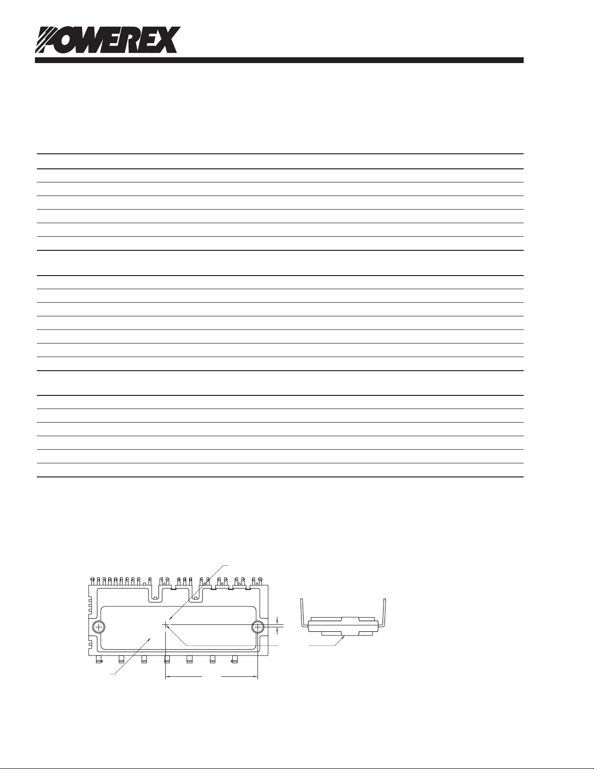
IGBT CHIP
BUILT-IN HEATSINK
1.2
40.5
TC POINT
PS21A79
Intellimod™ Module
Dual-In-Line Intelligent Power Module
50 Amperes/600 Volts
Absolute Maximum Ratings, Tj = 25°C unless otherwise specified
Characteristics Symbol PS21A79 Units
Self-protection Supply Voltage Limit (Short Circuit Protection Capability)* V
400 Volts
CC(prot.)
Module Case Operation Temperature (See TC Measurement Point Below) TC -20 to 100 °C
Storage Temperature T
-40 to 125 °C
stg
Mounting Torque, M4 Mounting Screws — 13 in-lb
Module Weight (Typical) — 65 Grams
Isolation Voltage, AC 1 minute, 60Hz Sinusoidal, Connection Pins to Heatsink Plate V
2500 Volts
ISO
IGBT Inverter Sector
Supply Voltage (Applied between P-NU, NV, NW) VCC 450 Volts
Supply Voltage, Surge (Applied between P-NU, NV, NW) V
CC(surge)
Collector-Emitter Voltage (TC = 25°C) V
Collector Current (TC = 25°C) ±IC 50 Amperes
Peak Collector Current (TC = 25°C, <1ms) ±ICP 100 Amperes
Collector Dissipation (TC = 25°C, per 1 Chip) PC 142 Watts
Power Device Junction Temperature** Tj -20 to 150 °C
500 Volts
600 Volts
CES
Control Sector
Supply Voltage (Applied between VP1-VPC, VN1-VNC) VD 20 Volts
Supply Voltage (Applied between V
UFB-VUFS, VVFB-VVFS
, V
WFB-VWFS
) VDB 20 Volts
Input Voltage (Applied between UP, VP, WP-VPC, UN, VN, WN-VNC) VIN -0.5 ~ VD+0.5 Volts
Fault Output Supply Voltage (Applied between FO-VNC) VFO -0.5 ~ VD+0.5 Volts
Fault Output Current (Sink Current at FO Terminal) IFO 1 mA
Current Sensing Input Voltage (Applied between CIN-VNC) VSC -0.5 ~ VD+0.5 Volts
*VD = 13.5 ~ 16.5V, Inverter Part, Tj = 125°C, Non-repetitive, Less than 2µs
**The maximum junction temperature rating of the power chips integrated within the DIPIPM is 150°C (@Tf ≤ 100°C). However, to ensure safe operation of the DIPIPM,
the average junction temperature should be limited to T
≤ 125°C (@Tf ≤ 100°C).
j(avg)
TC Measurement Point
2 Rev. 08/09
Page 4

Powerex, Inc., 173 Pavilion Lane, Youngwood, Pennsylvania 15697 (724) 925-7272
PS21A79
Intellimod™ Module
Dual-In-Line Intelligent Power Module
50 Amperes/600 Volts
Electrical and Mechanical Characteristics, Tj = 25°C unless otherwise specified
Characteristics Symbol Test Conditions Min. Typ. Max. Units
IGBT Inverter Sector
Collector-Emitter Saturation Voltage V
IC = 50A, Tj = 125°C, VD = VDB = 15V, VIN = 5V — 1.65 2.10 Volts
Diode Forward Voltage VEC T
Inductive Load Switching Times ton 1.80 2.40 — µs
t
t
t
t
Collector-Emitter Cutoff Current I
V
IC = 50A, Tj = 25°C, VD = VDB = 15V, VIN = 5V — 1.55 2.05 Volts
CE(sat)
= 25°C, -IC = 50A, VIN = 0V — 1.70 2.20 Volts
j
V
rr
I
C(on)
Inductive Load (Upper-Lower Arm) — 3.00 — µs
off
C(off)
V
CES
= 300V, VD = VDB = 15V, — 0.30 — µs
CC
= 50A, Tj = 125°C, VIN = 0 ⇔ 5V, — 0.40 — µs
C
— 0.65 — µs
= V
CE
CE
, Tj = 25°C — — 1.0 mA
CES
= V
, Tj = 125°C — — 10 mA
CES
Control Sector
Circuit Current I
D
Total of VP1-VPC, VN1-V
V
V
Total of VP1-VPC, VN1-V
V
V
Fault Output Voltage V
V
VSC = 0V, FO Terminal Pull-up to 5V by 10kΩ 4.9 — — Volts
FOH
V
FOL
Input Current IIN V
Short-Circuit Trip Level* ISC -20°C ≤ TC ≤ 100°C, VD = 15V, RS = 21.5Ω 85.0 — 150.0 Amps
Supply Circuit Undervoltage UV
Protection UV
Trip Level, TC ≤ 100°C 10.0 — 12.0 Volts
DBt
Reset Level, TC ≤ 100°C 10.5 — 12.5 Volts
DBr
UVDt Trip Level, TC ≤ 100°C 10.3 — 12.5 Volts
UVDr Reset Level, TC ≤ 100°C 10.8 — 13.0 Volts
Fault Output Pulse Width** tFO C
ON Threshold Voltage V
OFF Threshold Voltage V
Applied between UP, VP, WP-V
th(on)
U
th(off)
Temperature Output VOT At LVIC Temperature = 85°C 3.50 3.63 3.76 Volts
* Short-Circuit protection is functioning only at the lower ar ms. Please select the value of the external shunt resistor such that the SC trip level is less than 85A.
**Fault signal is asserted when the lower arm shor t circuit or control supply under-voltage protective functions operate. The fault output pulse-width tFO depends on the capacitance value
of CFO according to the following approximate equation: CFO = (12.2 x 10⁻⁶ x tFO [F]).
***When the temperature rises excessively, the controller (MCU) should stop the DIPIPM.
VD = VDB = 15V, VIN = 5V, — — 7.00 mA
NC
= VDB = 15V, VIN = 5V, — — 0.55 mA
D
UFB-VUFS
, V
VFB-VVFS
, V
WFB-VWFS
VD = VDB = 15V, VIN = 0V, — — 7.00 mA
NC
= VDB = 15V, VIN = 0V, — — 0.55 mA
D
UFB-VUFS
, V
VFB-VVFS
= 1V, IFO = 1mA — — 0.95 Volts
SC
IN
FO
, VN, WN-VNC 0.8 1.4 2.1 Volts
N
, V
WFB-VWFS
= 5V 1.0 1.5 2.0 mA
= 22nF 1.0 1.8 — ms
2.1 2.3 2.6 Volts
PC,
3Rev. 08/09
Page 5
Powerex, Inc., 173 Pavilion Lane, Youngwood, Pennsylvania 15697 (724) 925-7272
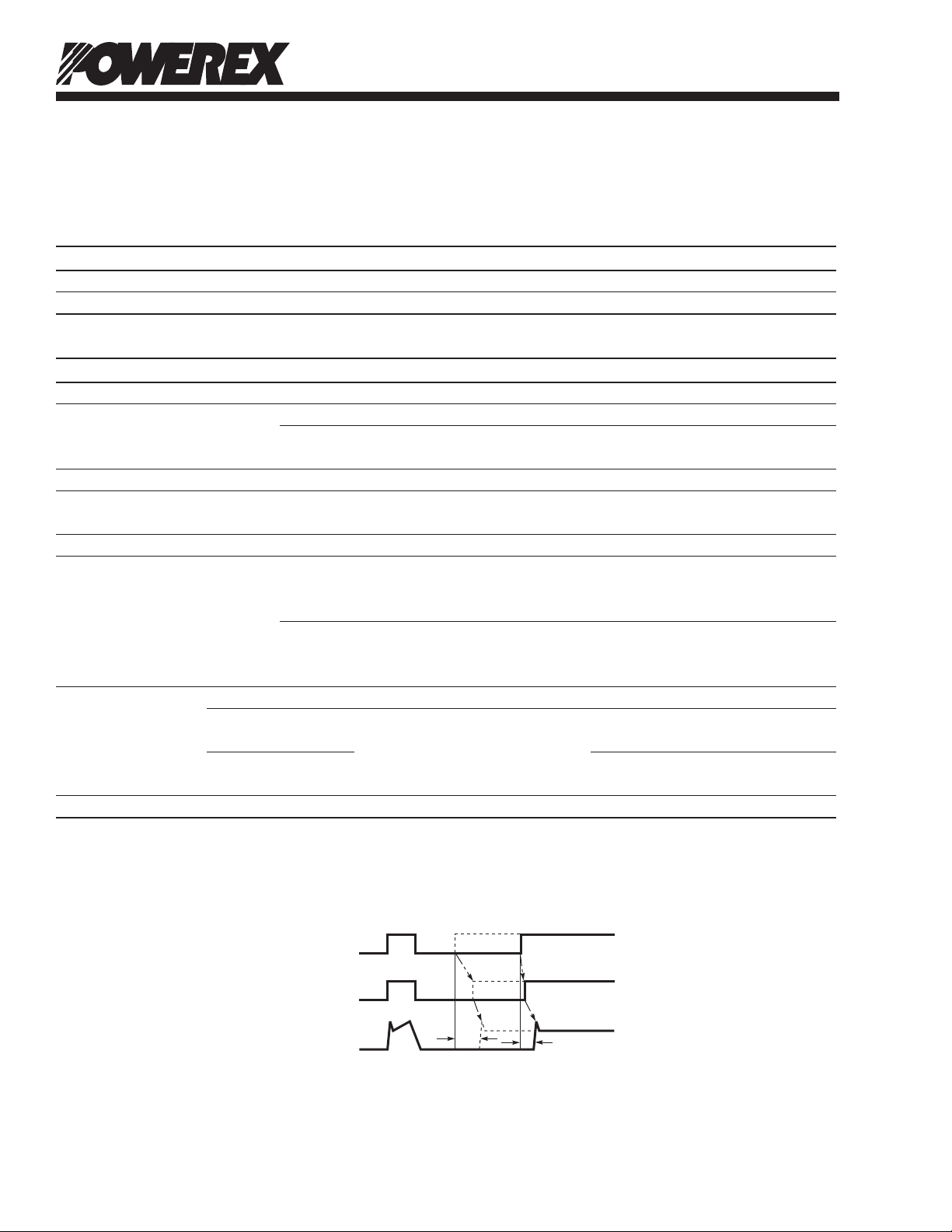
t2
t1
P-SIDE
CONTROL INPUT
INTERNAL
IGBT GATE
OUTPUT
CURRENT I
C
Solid Line – OFF Pulse Width > P
WIN(off)
: Turn ON time t1.
Dotted Line – OFF Pulse Width < P
WIN(off)
: Turn ON time t2.
PS21A79
Intellimod™ Module
Dual-In-Line Intelligent Power Module
50 Amperes/600 Volts
Thermal Characteristics, Tj = 25°C unless otherwise specified
Characteristic Symbol Condition Min. Typ. Max. Units
Thermal Resistance Junction to Case R
Thermal Resistance Junction to Case R
IGBT Part (Per 1/6 Module) — — 0.88 °C/Watt
th(j-C)Q
FWDi Part (Per 1/6 Module) — — 1.78 °C/Watt
th(j-C)D
Recommended Conditions for Use
Characteristic Symbol Condition Min. Typ. Max. Units
Supply Voltage VCC Applied between P-NU, NV, NW 0 300 400 Volts
Control Supply Voltage VD Applied between VP1-VPC, VN1-VNC 13.5 15.0 16.5 Volts
V
V
Control Supply Variation
ΔVD, ΔVDB -1 — 1 V/µs
Arm Shoot-through t
Blocking Time
PWM Input Frequency f
Allowable rms Current* IO V
f
T
V
f
T
Minimum Input P
Pulse Width P
50 ≤ IC ≤ 85A 13.5 ≤ VDB ≤ 18.5V, -20°C ≤ TC ≤ 100°C, 5.0 — — µs
N-line Wiring Inductance Less Than 10nH
VNC Variation VNC Between VNC-NU, NV, NW (Including Surge) -5.0 — 5.0 Volts
* The allowable rms current value depends on the actual application conditions.
**If input signal ON pulse is less than P
***The IPM may fail to respond to an ON pulse if the preceeding OFF pulse is less than P
WIN(on)
Applied between V
DB
VFB-VVFS
For Each Input Signal, TC ≤ 100°C 2.0 — — µs
DEAD
T
PWM
PWM
PWM
** 0.3 — — µs
WIN(on)
WIN(off)***
≤ 100°C, Tj ≤ 125°C — — 20 kHz
C
= 300V, VD = 15V, — — 23.6 Arms
CC
= 5kHz, PF = 0.8, Sinusoidal PWM,
≤ 125°C, TC ≤ 100°C
j
= 300V, VD = 15V, — — 13.8 Arms
CC
= 15kHz, PF = 0.8, Sinusoidal PWM,
≤ 125°C, TC ≤ 100°C
j
UFB-VUFS,
, V
WFB-VWFS
13.0 15.0 18.5 Volts
IC ≤ 50A 200 ≤ VCC ≤ 350V, 13.5 ≤ VD ≤ 16.5V, 3.0 — — µs
, the device may not respond.
WIN(off)
.
Delayed Response Against Shorter Input OFF Signal Than P
4 Rev. 08/09
WIN
, P-side only
(off)
Page 6
Powerex, Inc., 173 Pavilion Lane, Youngwood, Pennsylvania 15697 (724) 925-7272
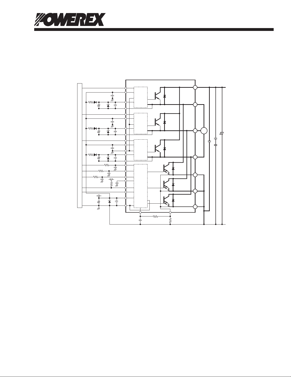
Component Selection:
Dsgn. Typ. Value Description
D1 1A, 600V Control and boot strap supply overvoltage suppression
DZ1 24V, 1W Control and boot strap supply over voltage suppression
C1 10-100µF, 50V Boot strap supply reservoir – electrolytic long lifem low impedance, 105°C
C2 0.22-2.0µF, 50V Local decoupling/High frequency noise filters – multilayer ceramic (Note 4)
C3 200 to 2500µF, 450V Main DC bus filter capacitor – electrolytic, long life, high ripple current, 105°C
C4 100pF, 50V Optional input signal noise filter – multilayer ceramic (Note 11)
C5 0.1-0.22µF, 1000V Surge voltage suppression (Note 2)
CSF 1000pF, 50V Shor t circuit detection filter capacitor – multilayer ceramic
RSF 1.8kΩ Short circuit detection filter resistor
R
SHUNT
20ohm-500ohm Current sensing resistor
R1 1-10Ω Boot strap supply inrush limiting resistor – non-inductive, temperature stable, tight tolerance (Note 5)
R2 330Ω Optional input signal noise filter (Note 11)
R3 10kΩ Fault signal pull-up resistor (Note 9)
Notes:
1) If control GND is connected to power GND by broad pattern, it may cause malfunction by power GND fluctuation.
It is recommended to connect control GND at only a point at which NU, NV, NW are connected to power GND line.
2) To prevent surge destruction, the wiring between the smoothing capacitor and the P-N1 terminals should be as short as
possible. Generally inserting a 0.1µ ~ 0.22µF snubber capacitor C3 between the P-N1 terminals is recommended.
3) The time constant R1,C4 of RC filter for preventing the protection circuit malfunction should be selected in the range of 1.5µ ~ 2µs.
SC interrupting time might vary with the wiring pattern. Tight tolerance, temp-compensated type is recommended for R1,C4.
4) All capacitors should be mounted as close to the terminals of the DIPIPM as possible. (C1: good temperature, frequency
characteristics electrolytic type, and C2 : good temperature, frequency and DC bias characteristic ceramic type are recommended.)
5) It is recommended to insert a Zener diode DZ1 (24V/1W) between each pair of control supply terminals to prevent surge destruction.
6) To prevent erroneous SC protection, the wiring from VSC terminals to CIN filter should be divided at the point D that is close
to the terminal of sense resistor and the wiring should be patterned as short as possible.
7) For sense resistor, the variation within 1% (including temperature characteristics), low inductance type is recommended.
1/8W is recommended, but an evaluation of your system is recommended.
8) To prevent erroneous operation, wiring A, B, and C should be as short as possible.
9) FO output is open drain type. It should be pulled up to the positive side of 5V or 15V power supply with a resistor that limits
FO sink current (IFO) under 1mA. (Over 5.1kΩ is needed and 10kΩ is recommended for 5V supply.)
10) Error signal output width (tFO) can be set by the capacitor connected to the CFO terminal. t
FO(typ)
= CFO / 9.1 x 10⁻⁶ (s).
11) Input drive is high-active type. There is a 3.3kΩ pull-down resistor integrated in the IC input circuit. To prevent malfunction, the wiring of each input
should be patterned as short as possible. When inserting the RC filter, make sure the input signal level meets the turn-on and turn-off threshold voltage.
Thanks to HVIC inside the module, connection to the MCU may be direct or with an opto-coupler.
V
N1
U
N
F
O
V
OT
V
NC
V
NO
V
SC
D
B
C
A
R
SHUNT
C
IN
C
SF
R
SF
V
N
W
N
CFO
HVIC1
IGBT1
FWDi1
IGBT2
FWDi2
IGBT3
IGBT4
IGBT5
IGBT6
FWDi3
FWDi4
FWDi5
FWDi6
LVIC
P
U
HVIC2
V
V
WFB
V
P1
V
WFS
W
P
V
PC
HVIC3
W
NU
NV
NW
C
2DZ1
C
1
V
D
15V
+
+
C
2
C
4
C
4
C
4
R
3
R
2
R
2
R
2
C
2
DZ
1
C
1
D
1
+
V
VFB
V
P1
V
VFS
V
P
C
2
C
2
DZ
1
C
1
D
1
MCU
+
V
UFB
V
P1
V
UFS
U
P
C
2
C
2
C
3
C
3
C
5
DZ
1
C
1
D
1
+
M
PS21A79
Intellimod™ Module
Dual-In-Line Intelligent Power Module
50 Amperes/600 Volts
Application Circuit
5Rev. 08/09
Page 7

Powerex, Inc., 173 Pavilion Lane, Youngwood, Pennsylvania 15697 (724) 925-7272
a1
SC
SC REFERENCE VOLTAGE
RC CIRCUIT TIME CONSTANT DELAY
a2
a3
a4
a8
a5
a7a6
SET
RESET
N-SIDE
CONTROL INPUT
PROTECTION
CIRCUIT STATE
INTERNAL IGBT GATE
SENSE VOLTAGE OF R
S
OUTPUT CURRENT I
C
FAULT OUTPUT F
O
Short Circuit Protection (N-side Only with External Shunt Resistor and RC Filter)
a1: Normal operation – IGBT turns on and carries current.
a2: Short circuit current is detected (SC trigger).
a3: All N-side IGBT's gate are hard interrupted.
a4: All N-side IGBT's turn off.
a5: FO output wirh a fixed pulse width (determined by the external capacitance CFO).
a6: Input "L" – IGBT off.
a7: Input "H" – IGBT on, but during the FO output perid the IGBT will not turn on.
a8: IGBT turns on when L→H signal is input after FO is reset.
b1
b4
b5
b2
UV
Dt
b7
b3
SET
RESETRESET
UV
Dr
b6
CONTROL INPUT
PROTECTION
CIRCUIT STATE
CONTRO L SUPPLY
VOLTAGE V
D
OUTPUT CURRENT I
C
FAULT OUTPUT F
O
Under-Voltage Protection (N-side , UVD)
b1: Control supply voltage VD rises – After VD level reaches under voltage reset level (UVDr), the circuits
start to operate when next input is applied.
b2 : Normal operation – IGBT turns on and carries current.
b3: VD level dips to under voltage trip level (UVDt).
b4: All N-side IGBT’s turn off in spite of control input condition.
b5: FO is low for a minimum period determined by the capacitance CFO but continuously during UV period.
b6: VD level reaches UVDr.
b7: Normal operation – IGBT turns on and carries current.
PS21A79
Intellimod™ Module
Dual-In-Line Intelligent Power Module
50 Amperes/600 Volts
Protection Function Timing Diagrams
6 Rev. 08/09
Page 8

Powerex, Inc., 173 Pavilion Lane, Youngwood, Pennsylvania 15697 (724) 925-7272
c1
c5
c6
c3
c2
UV
Dt
c4
SET
RESETRESET
HIGH LEVEL (NO FAULT OUTPUT)
UV
DBr
CONTROL INPUT
PROTECTION
CIRCUIT STATE
CONTROL SUPPLY
VOLTAGE V
DB
OUTPUT CURRENT I
C
FAULT OUTPUT F
O
Under-Voltage Protection (P-side, UVDB)
c1: Control supply voltage VDB rises – After VDB level reaches under voltage reset level (UV
DBr
),
the circuits starts to operate when next input is applied.
c2: Normal operation – IGBT turns on and carries current.
c3: V
DB
level dips to under voltage trip level (UV
DBt
).
c4: P-side IGBT turns off in spite of control input signal level, but there is no FO signal output.
c5: V
DB
level reaches UV
DBr
.
c6: Normal operation – IGBT on and carries current.
UP, VP, WP, UN, VN, W
N
MCU
5V LINE
10kΩ
2.5kΩ (MIN)
F
O
VNC (LOGIC)
DIP-IPM
NOTE: RC coupling at each input
(parts shown dotted) may change
depending on the PWM control
scheme used in the application and
the wiring impedance of the printed
circuit board. The DIPIPM input signal
section integrates a 2.5k
Ω (min)
pull-down resistor. Therefore, when
using an external filtering resistor, care
must be taken to satisfy the turn-on
threshold voltage requirement.
V
NC
NW
NV
NU
DIPIPM
It is recommended to make the inductance under 10nH.
For shunt resistors, it is recommended to use as low
inductance type as possible.
Shunt
Resistors
Connect the wiring from VNC terminal at the point as
close to shunt resistors’ terminal as possible.
It is recommended to divide the wiring to current detecting
circuit at the point as close to shunt resistor’s terminal as
possible.
To Current
Detecting Circuit
PS21A79
Intellimod™ Module
Dual-In-Line Intelligent Power Module
50 Amperes/600 Volts
Protection Function Timing Diagrams
Typical Interface Circuit
Wiring Method Around Shunt Resistor
7Rev. 08/09
 Loading...