

Page 1

6121 Baker Road,
Suite 108
Minnetonka, MN 55345
www.chtechnology.com
Phone (952) 933-6190
Fax (952) 933-6223
1-800-274-4284
Thank you for downloading this document from C&H Technology, Inc.
Please contact the C&H Technology team for the following questions -
Technical
Application
Assembly
Availability
Pricing
Phone – 1-800-274-4284
E-Mail – sales@chtechnology.com
www.chtechnology.com - SPECIALISTS IN POWER ELECTRONIC COMPONENTS AND ASSEMBLIES - www.chtechnology.com
Page 2
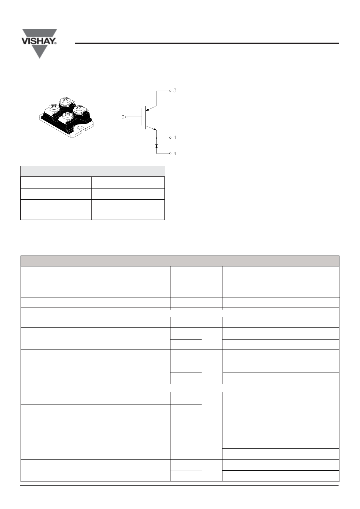
SOT-227
PRODUCT SUMMARY
Target Data 03/09
GT100NA120U
Vishay Semiconductor Italy
SOT 227 TRENCH IGBT, 100 A
High Side Chopper
Features
• Trench IGBT
• Very Low VCE
• 10 μs short circuit capability
• Hexfred clamping diode
• Minimal tail current
• Tighter distribution of parameters
• Higher reliability
• Electronic Power Supplies application
(ON)
I
C(DC)
I
F(DC)
V
CE(on) typ
V
CES
Absolute Maximum Ratings indicate sustained limits beyond which damage to the device may occur. All currents are
defined positive into any lead. The Thermal Resistance and Power Dissipation ratings are measured under board mounted
and still air conditions.
111 A @ 70°C
65 A @ 70°C
2.36 V @ 100 A, 25°C
1200V
Benefits
• Lower conduction losses and switching losses
• Higher switching frequency up to 25 KHz
ABSOLUTE MAXIMUMRATINGS
PARAMETERS VALUES UNITS CONDITIONS
T
J
T
STG
V
ISOL
Diode
V
RRM
I
FM
I
FSM
P
D
Maximum operating junction temperature 150 °C
Storage temperature range -55 to150
RMS isolation voltage, Any terminal to case 2500 V t = 1min, TJ = 25°C
Repetitive peak reverse voltage 1200 V
Continuous forward current 88 A TC = 25°C
60 TC = 80°C
Non repetitive peak surge current 400 A TJ = 25°C, 10 ms
Maximum power dissipation 338 W TC = 25°C
189 TC = 80°C
IGBT
V
CES
V
GES
I
CM
I
LM
I
C
P
D
Revision: 18-Mar-09
Collector to Emitter Voltage 1200 V
Gate to Emitter Voltage 20
Pulse collector current 270 A
Clump inductive load current 270 A
Continuous collector current 148 A TC = 25°C
Maximum power dissipation 521 W TC = 25°C
102 TC = 80°C
292 TC = 80°C
1
Page 3

GT100NA120U
Vishay Semiconductor Italy
THERMAL-MECHANICAL SPECIFICATION
PARAMETERS MIN TYP MAX UNITS
R
thCS
Case-to-Sink, flat, greased surface 0.05 °C/ W
T Mounting torque (M3 screw) 1.3 Nm
Wt Weight 30 g
Diode
R
thJC
Junction-to-Case, diode thermal resistance 0.37 °C/ W
IGBT
R
thJC
Junction-to-Case, IGBT thermal resistance 0.24 °C/ W
ELECTRICAL CHARACTERISTICS @ TJ = 25°C (unless otherwise specified)
PARAMETERS MIN TYP MAX UNITS TEST CONDITIONS
Clamping Diode
I
RM
V
FM
IGBT
BV
CES
ΔV
BR(CES)
V
CE(on)
V
GE(th)
ΔV
GE(th)
I
CES
I
GES
Reverse leakage current 10 μA 1200V
0.5 mA 1200V, TJ = 125°C
Forward voltage drop 4.4 V IC = 100A
5.2 IC = 100A, TJ = 125°C
Collector to emitter breakdown volt. 1200 V VGE = 0V, IC = 500μA
/ΔTJTemp. coefficient of breakdown 0.05 V/°C VGE = 0V, IC = 1mA (25°C-150°C)
Collector to emitter voltage 1.79 VGE = 15V, IC = 50A
2.4 V VGE = 15V, IC = 100A
2.0 VGE = 15V, IC = 50A TJ = 125°C
2.7 VGE = 15V, IC = 100A
Gate threshold voltage 5.8 V VCE = VGE, IC = 500μA
/ΔTJTemp.coeff. of threshold voltage -30 mV/°C VCE = VGE, IC = 1mA (25°C-150°C)
Zero gate voltage collector current 10 μAVGE = 0V, VCE = 1200V
100 VGE = 0V, VCE = 1200V, TJ = 125°C
Gate to emitter leakage current ± 200 nALoAVGE = ± 20V
2
Revision 18-Mar-09
Page 4

SWITCHING CHARACTERISTICS @ TJ = 25°C (unless otherwise specified)
PARAMETERS MIN TYP MAX UNITS TEST CONDITIONS
IGBT Switch
Q
g
Q
ge
Q
gc
E
on
E
off
E
ts
E
on
E
off
E
ts
t
d(on)
t
r
t
d(off)
t
f
RBSOA Reverse Bias safe operating area full square
I
rr
t
rr
Q
rr
Total Gate Charge (turn-on) 400 IC = 100A, VGE = 15V, VCC = 600V
Gate-Emitter Charge (turn-on) 120 nC
Gate-Collector Charge (turn-on) 170
Turn-On Switching Loss 21 IC = 100A
Turn-Off Switching Loss 5.5 mJ VGE = 15V, Rg = 5Ω
Total Switching Loss 26.5 L = 500μH
Turn-On Switching Loss 23.6
Turn-Off Switching Loss 7.6 mJ IC = 100A, VCC = 600V
Total Switching Loss 31.2 VGE = 15V, Rg = 5Ω
Turn-on Delay Time 195 ns L = 50 0μH, TJ = 125°C
Rise Time 280
Turn-off Delay Time 187
Fall Time 225
TJ = 150°C, IC = 270A,
Rg = 22 Ω, VGE = 15 to 0V
Diode
Peak reverse recovery current 11 A TJ = 25°C
18 TJ = 125°C
Reverse recovery time 128 ns TJ = 25°C IF = 50A, VR = 200V
208 T
= 125°C dI/dt = 200A/μs
J
Reverse recovery charge 704 nC TJ = 25°C
1872 TJ = 125°C
GT100NA120U
Vishay Semiconductor Italy
3Revision 18-Mar-09
Page 5

GT100NA120U
Vishay Semiconductor Italy
OUTLINE TABLE
SOT-227 Package Details
Dimensions are shown in millimeters ( inches )
4.40 (.173 )
4.20 (.165 )
12.50 ( .492 )
7.50 ( .295 )
2.10 ( .082 )
1.90 ( .075 )
4
1
38.30 ( 1.508 )
37.80 ( 1.488 )
-A-
30.20 ( 1.189 )
29.80 ( 1.173 )
4X
3
2
8.10 ( .319 )
7.70 ( .303 )
CHAMFER
2.00 ( .079 ) X 457
6.25 ( .246 )
15.00 ( .5 90 )
2.10 ( .0 82 )
1.90 ( .0 75 )
25.70 ( 1.012 )
25.20 ( .992 )
-B-
4
1
R FULL
0.25 ( .010 ) M C A M B M
-C-
0.12 ( .005 )
LEAD ASSIGMENTS
C
E
G
E
IGBT
A1
K2
3
2
K1 A2
HEXFRED
A
S
4
1
E,K
HEXFET
12.30 ( .484 )
11.80 ( .464 )
C
D
3
2
GS
G
Tube
QUANTITIES PER TUBE IS 10
M4 SREW AND WASHER INCLUDED
4
Revision 18-Mar-09
Page 6

ORDERING INFORMATION TABLE
Device Code
G T 100 N A 120 U
GT100NA120U
Vishay Semiconductor Italy
1
2 3
1 - Insulated Gate Bipolar Transistor (IGBT)
2 - T = Trench IGBT
3 - Current Rating (100 = 100 A)
4 - Circuit Configuration (N = High Side Chopper)
5 - Package Indicator (A = SOT-227)
6 Voltage Rating (120 = 1200V)
7 - Speed/ Type (U = Ultra Fast IGBT)
4
6
5
7
5Revision 18-Mar-09
 Loading...