

C&H Technology GT100DA60U User Manual

6121 Baker Road,
Suite 108
Minnetonka, MN 55345
www.chtechnology.com
Phone (952) 933-6190
Fax (952) 933-6223
1-800-274-4284
Thank you for downloading this document from C&H Technology, Inc.
Please contact the C&H Technology team for the following questions -
Technical
Application
Assembly
Availability
Pricing
Phone – 1-800-274-4284
E-Mail – sales@chtechnology.com
www.chtechnology.com - SPECIALISTS IN POWER ELECTRONIC COMPONENTS AND ASSEMBLIES - www.chtechnology.com
www.vishay.com
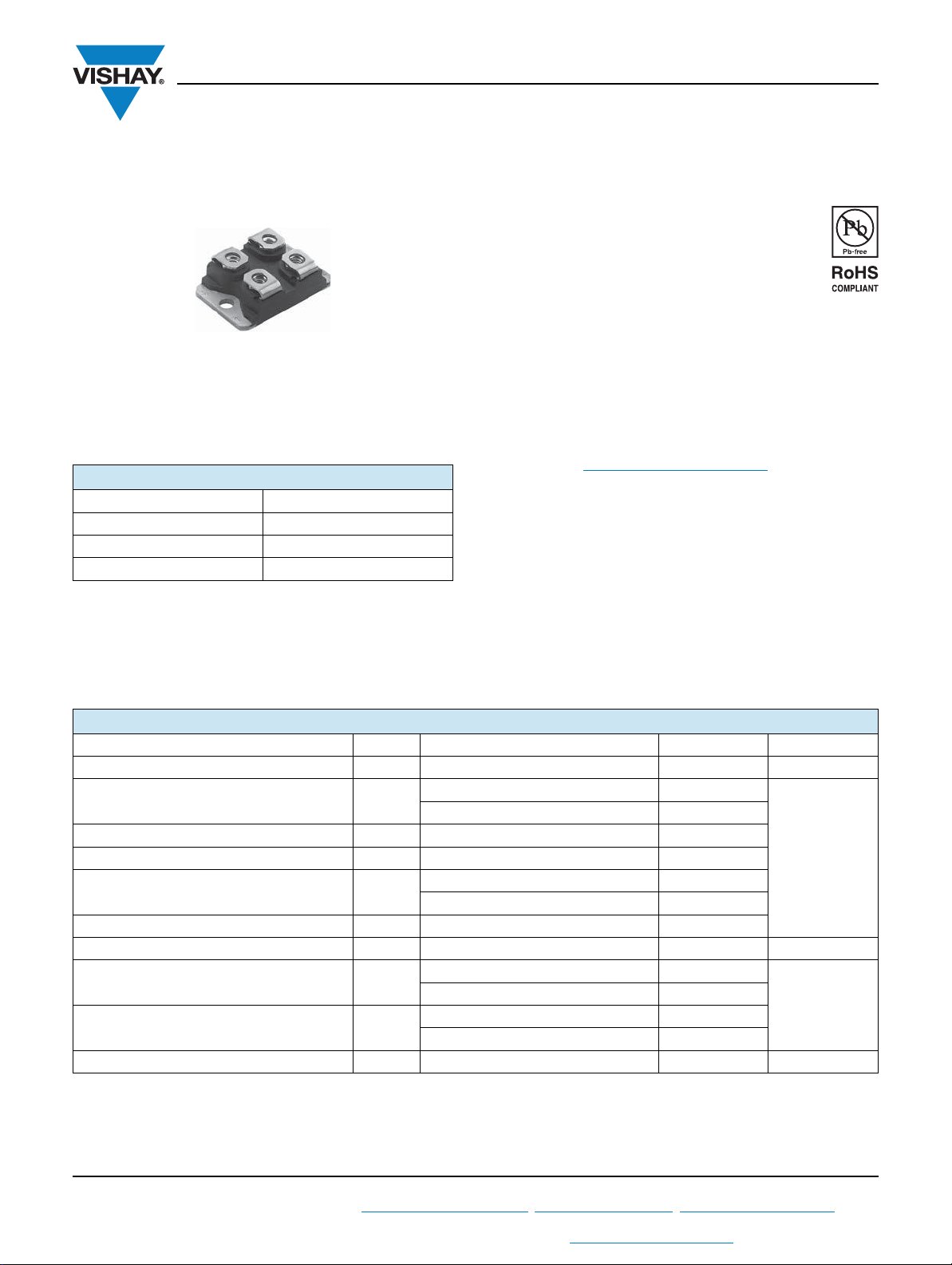
SOT-227
Insulated Gate Bipolar Transistor
PRODUCT SUMMARY
V
CES
I
DC 100 A at 117 °C
C
typical at 100 A, 25 °C 1.72 V
V
CE(on)
I
DC 100 A at 25 °C
F
(Trench IGBT), 100 A
FEATURES
• Trench IGBT technology with positive
temperature coefficient
•Square RBSOA
• 3 μs short circuit capability
®
600 V
•FRED Pt
reverse recovery
•TJ maximum = 175 °C
• Fully isolated package
• Very low internal inductance ( 5 nH typical)
• Industry standard outline
• Material categorization: For definitions of compliance
please see www.vishay.com/doc?99912
BENEFITS
• Designed for increased operating efficiency in power
conversion: UPS, SMPS, welding, induction heating
• Easy to assemble and parallel
• Direct mounting to heatsink
• Plug-in compatible with other SOT-227 packages
• Speed 4 kHz to 30 kHz
• Lower conduction losses and switching losses
• Low EMI, requires less snubbing
GT100DA60U
Vishay Semiconductors
antiparallel diodes with ultrasoft
ABSOLUTE MAXIMUM RATINGS
PARAMETER SYMBOL TEST CONDITIONS MAX. UNITS
Collector to emitter voltage V
Continuous collector current I
Pulsed collector current I
Clamped inductive load current I
Diode continuous forward current I
Peak diode forward current I
Gate to emitter voltage V
Power dissipation, IGBT P
Power dissipation, diode P
Isolation voltage V
Note
(1)
Maximum continuous collector current must be limited to 100 A to do not exceed the maximum temperature of terminals
Revision: 24-Oct-12
For technical questions within your region: DiodesAmericas@vishay.com
THIS DOCUMENT IS SUBJECT TO CHANGE WITHOUT NOTICE. THE PRODUCTS DESCRIBED HEREIN AND THIS DOCUMENT
ARE SUBJECT TO SPECIFIC DISCLAIMERS, SET FORTH AT www.vishay.com/doc?91000
CES
C
CM
LM
F
FSM
GE
ISOL
TC = 25 °C 184
(1)
T
= 80 °C 137
C
TC = 25 °C 100
T
= 80 °C 71
C
TC = 25 °C 577
D
D
= 117 °C 223
T
C
TC = 25 °C 205
= 117 °C 79
T
C
Any terminal to case, t = 1 min 2500 V
1
, DiodesAsia@vishay.com, DiodesEurope@vishay.com
600 V
350
350
200
± 20 V
Document Number: 93185
A
W
GT100DA60U
www.vishay.com
ELECTRICAL SPECIFICATIONS (TJ = 25 °C unless otherwise specified)
PARAMETER SYMBOL TEST CONDITIONS MIN. TYP. MAX. UNITS
Collector to emitter breakdown voltage V
BR(CES)
VGE = 0 V, IC = 250 μA 600 - -
VGE = 15 V, IC = 100 A - 1.72 2.0
Gate threshold voltage V
Temperature coefficient of
threshold voltage
V
GE(th)
Collector to emitter leakage current I
Forward voltage drop V
Gate to emitter leakage current I
CE(on)
GE(th)
/TJVCE = VGE, IC = 1 mA (25 °C to 125 °C) - - 16.8 - mV/°C
CES
FM
GES
= 15 V, IC = 100 A, TJ = 125 °C - 2.0 2.2
V
GE
VCE = VGE, IC = 250 μA 3.5 4.6 6.5
VGE = 0 V, VCE = 600 V - 0.6 100 μA
= 0 V, VCE = 600 V, TJ = 125 °C - 0.15 3 mA
V
GE
IF = 40 A, VGE = 0 V - 1.78 2.21
= 40 A, VGE = 0 V, TJ = 125 °C - 1.39 1.74
I
F
VGE = ± 20 V - - ± 200 nA
SWITCHING CHARACTERISTICS (TJ = 25 °C unless otherwise specified)
PARAMETER SYMBOL TEST CONDITIONS MIN. TYP. MAX. UNITS
Turn-on switching loss E
Turn-off switching loss E
Total switching loss E
Turn-on switching loss E
Turn-off switching loss E
Total switching loss E
Turn-on delay time t
Rise time t
Turn-off delay time t
Fall time t
Reverse bias safe operating area RBSOA
Diode reverse recovery time t
Diode peak reverse current I
Diode recovery charge Q
Diode reverse recovery time t
Diode peak reverse current I
Diode recovery charge Q
Short circuit safe operating area SCSOA
on
off
tot
on
off
tot
d(on)
d(off)
rr
rr
rr
rr
IC = 100 A, VCC = 360 V,
V
= 15 V, Rg = 5
GE
L = 500 μH, T
= 25 °C
J
Energy losses
include tail and
IC = 100 A, VCC = 360 V,
V
= 15 V, Rg = 5
GE
r
f
L = 500 μH, T
= 175 °C, IC = 350 A, Rg = 22
T
J
V
= 15 V to 0 V, VCC = 400 V,
GE
= 600 V, L = 500 μH
V
P
= 125 °C
J
diode recovery
(see fig. 18)
IF = 50 A, dIF/dt = 200 A/μs, VR = 200 V
rr
IF = 50 A, dIF/dt = 200 A/μs,
V
= 200 V, TJ = 125 °C
R
rr
= 175 °C, Rg = 22 ,
T
J
V
= 15 V to 0 V, VCC = 400 V,
GE
= 600 V
V
p
Vishay Semiconductors
VCollector to emitter voltage V
V
-0.35-
-2.08-
-2.43-
-0.41-
-2.83-
-3.24-
- 162 -
-55-
- 150 -
- 129 -
Fullsquare
-6185ns
-47A
- 120 297 nC
- 133 154 ns
-1215A
- 750 1150 nC
3μs
mJ
ns
Revision: 24-Oct-12
For technical questions within your region: DiodesAmericas@vishay.com
2
, DiodesAsia@vishay.com, DiodesEurope@vishay.com
Document Number: 93185
THIS DOCUMENT IS SUBJECT TO CHANGE WITHOUT NOTICE. THE PRODUCTS DESCRIBED HEREIN AND THIS DOCUMENT
ARE SUBJECT TO SPECIFIC DISCLAIMERS, SET FORTH AT www.vishay.com/doc?91000
GT100DA60U
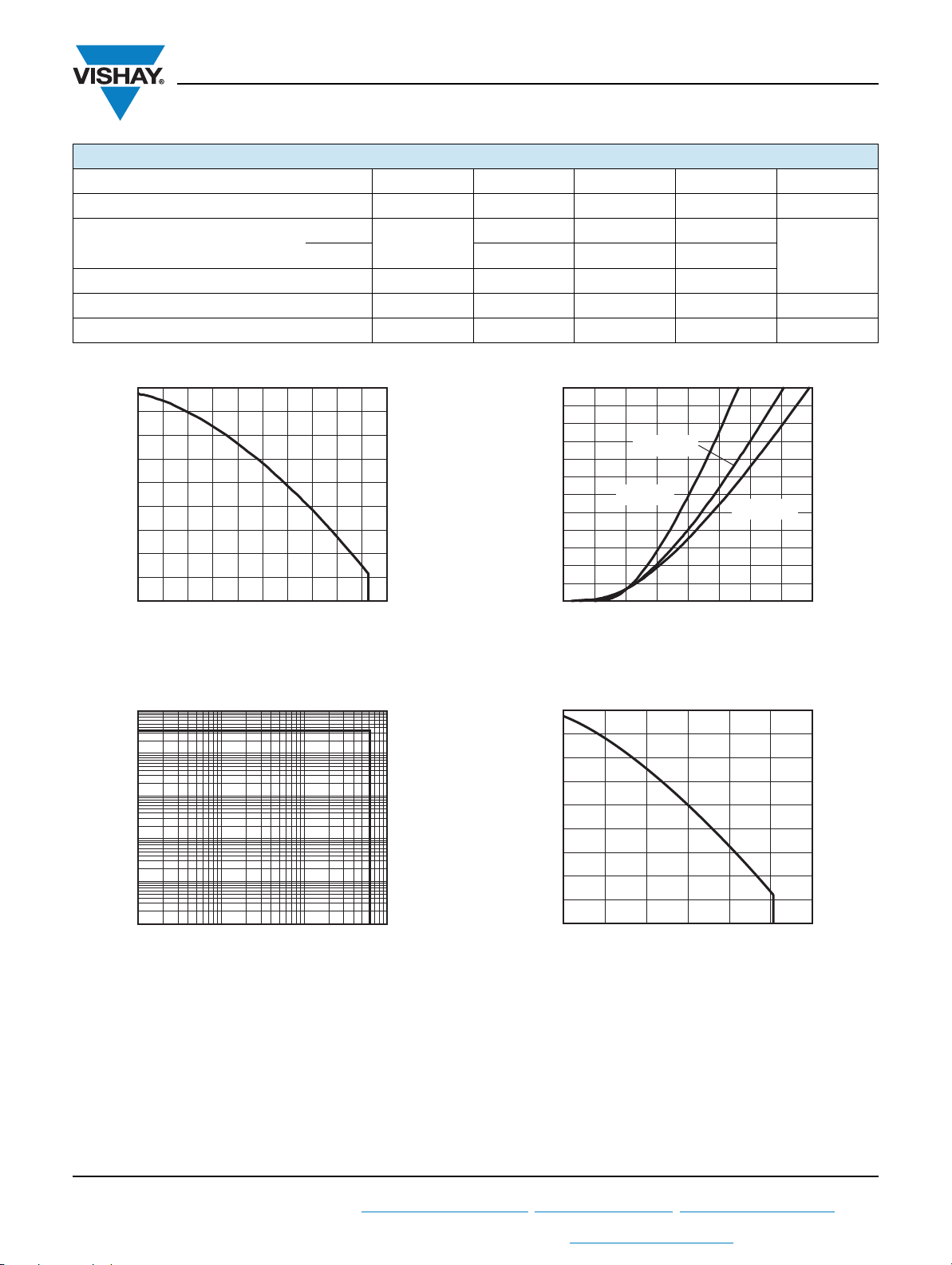
Allowable Case Temperature (°C)
IC - Continuous Collector Current (A)
0
93185_01
20 40 60 100 140 18080 120 160 200
0
180
160
100
120
140
20
40
60
80
I
C
(A)
VCE (V)
1 10 100 1000
0.01
0.1
1
93185_02
1000
10
100
Allowable Case Temperature (°C)
IF - Continuous Forward Current (A)
80604020 100
120
0
100
160
180
0
40
60
140
80
120
20
93185_04
www.vishay.com
THERMAL AND MECHANICAL SPECIFICATIONS
PARAMETER SYMBOL MIN. TYP. MAX. UNITS
Maximum junction and storage temperature range T
Junction to case
IGBT
Case to sink per module R
J
R
, T
thJC
thCS
Stg
Mounting torque, 6-32 or M3 screw - - 1.3 Nm
Weight - 30 - g
Fig. 1 - Maximum DC IGBT Collector Current vs.
Case Temperature
- 40 - 175 °C
- - 0.26
-0.05-
300
275
250
225
200
175
150
(A)
C
I
125
100
75
50
25
0
04.00.5 1.0 1.5 2.0 2.5 3.0 3.5
93185_02
Fig. 3 - Typical IGBT Collector Current Characteristics
Vishay Semiconductors
°C/WDiode - - 0.73
TJ = 125 °C
TJ = 25 °C
V
VCE (V)
= 15 V
GE
TJ = 175 °C
Fig. 2 - IGBT Reverse Bias SOA
Revision: 24-Oct-12
For technical questions within your region: DiodesAmericas@vishay.com
THIS DOCUMENT IS SUBJECT TO CHANGE WITHOUT NOTICE. THE PRODUCTS DESCRIBED HEREIN AND THIS DOCUMENT
T
= 175 °C, VGE = 15 V
J
Case Temperature
3
, DiodesAsia@vishay.com, DiodesEurope@vishay.com
Fig. 4 - Maximum DC Forward Current vs.
ARE SUBJECT TO SPECIFIC DISCLAIMERS, SET FORTH AT www.vishay.com/doc?91000
Document Number: 93185
 Loading...