

Page 1

6121 Baker Road,
Suite 108
Minnetonka, MN 55345
www.chtechnology.com
Phone (952) 933-6190
Fax (952) 933-6223
1-800-274-4284
Thank you for downloading this document from C&H Technology, Inc.
Please contact the C&H Technology team for the following questions -
Technical
Application
Assembly
Availability
Pricing
Phone – 1-800-274-4284
E-Mail – sales@chtechnology.com
www.chtechnology.com - SPECIALISTS IN POWER ELECTRONIC COMPONENTS AND ASSEMBLIES - www.chtechnology.com
Page 2
Insulated Gate Bipolar Transistor
(Ultrafast IGBT), 75 A
FEATURES
• NPT Generation V IGBT technology
• Square RBSOA
®
CE(on)
SOT-227
• HEXFRED
•Positive V
• Fully isolated package
• Speed 8 kHz to 60 kHz
• Very low internal inductance (≤ 5 nH typical)
• Industry standard outline
• Compliant to RoHS directive 2002/95/EC
GB75DA120UP
Vishay High Power Products
low Qrr, low switching energy
temperature coefficient
PRODUCT SUMMARY
V
CES
DC 75 A at 95 °C
I
C
typical at 75 A, 25 °C 3.3 V
V
CE(on)
1200 V
BENEFITS
• Designed for increased operating efficiency in power
conversion: UPS, SMPS, welding, induction heating
• Easy to assemble and parallel
• Direct mounting on heatsink
• Plug-in compatible with other SOT-227 packages
• Low EMI, requires less snubbing
ABSOLUTE MAXIMUM RATINGS
PARAMETER SYMBOL TEST CONDITIONS MAX. UNITS
Collector to emitter voltage V
Continuous collector current I
Pulsed collector current I
Clamped inductive load current I
Diode continuous forward current I
Gate to emitter voltage V
Power dissipation, IGBT P
Power dissipation, diode P
Isolation voltage V
CES
C
CM
LM
F
GE
D
D
ISOL
TC = 25 °C 131
= 80 °C 89
T
C
TC = 25 °C 59
= 80 °C 39
T
C
TC = 25 °C 658
= 80 °C 369
T
C
TC = 25 °C 240
= 80 °C 135
T
C
Any terminal to case, t = 1 min 2500 V
1200 V
200
200
± 20 V
A
W
Document Number: 93011 For technical questions, contact: ind-modules@vishay.com
Revision: 23-Apr-09 1
www.vishay.com
Page 3
GB75DA120UP
Vishay High Power Products
Insulated Gate Bipolar Transistor
(Ultrafast IGBT), 75 A
ELECTRICAL SPECIFICATIONS (TJ = 25 °C unless otherwise specified)
PARAMETER SYMBOL TEST CONDITIONS MIN. TYP. MAX. UNITS
Collector to emitter breakdown voltage V
Gate threshold voltage V
Temperature coefficient of
threshold voltage
Collector to emitter leakage current I
Forward voltage drop V
Gate to emitter leakage current I
BR(CES)VGE
CE(on)
GE(th)
V
/ΔTJVCE = VGE, IC = 1 mA (25 °C to 125 °C) - - 12 - mV/°C
GE(th)
CES
FM
GES
SWITCHING CHARACTERISTICS (TJ = 25 °C unless otherwise specified)
PARAMETER SYMBOL TEST CONDITIONS MIN. TYP. MAX. UNITS
Total gate charge (turn-on) Q
Gate to collector charge (turn-on) Q
Turn-on switching loss E
Turn-off switching loss E
Total switching loss E
Turn-on switching loss E
Turn-off switching loss E
Total switching loss E
Turn-on delay time t
Rise time t
Turn-off delay time t
Fall time t
Reverse bias safe operating area RBSOA
Diode reverse recovery time t
Diode peak reverse current I
Diode recovery charge Q
Diode reverse recovery time t
Diode peak reverse current I
Diode recovery charge Q
g
ge
gc
on
off
tot
on
off
tot
d(on)
r
d(off)
f
rr
rr
rr
rr
rr
rr
= 0 V, IC = 250 µA 1200 - -
VGE = 15 V, IC = 75 A - 3.3 3.8
= 15 V, IC = 75 A, TJ = 125 °C - 3.6 3.9
V
GE
VCE = VGE, IC = 250 µA 4 5 6
VGE = 0 V, VCE = 1200 V - 3 250 µA
= 0 V, VCE = 1200 V, TJ = 150 °C - 4 20 mA
V
GE
IC = 75 A, VGE = 0 V - 3.4 5.0
I
= 75 A, VGE = 0 V, TJ = 125 °C - 3.3 5.2
C
VGE = ± 20 V - - ± 200 nA
- 690 -
IC = 50 A, VCC = 600 V, VGE = 15 V
-65-
- 250 -
IC = 75 A, VCC = 600 V,
V
= 15 V, Rg = 5 Ω,
GE
L = 500 µH
IC = 75 A, VCC = 600 V,
V
= 15 V, Rg = 5 Ω,
GE
L = 500 µH, T
= 125 °C
J
Energy losses
include tail and
diode recovery
(see fig. 18)
-1.53-
-1.76-
-3.29-
-2.49-
-3.45-
-5.94-
- 281 -
-45-
- 300 -
- 126 -
= 150 °C, IC = 200 A, Rg = 22 Ω,
T
J
= 15 V to 0 V, VCC = 900 V,
V
GE
= 1200 V, L = 500 µH
V
P
Fullsquare
- 142 210 ns
IF = 50 A, dIF/dt = 200 A/µs, VR = 200 V
-1316A
- 923 1680 nC
- 202 260 ns
IF = 50 A, dIF/dt = 200 A/µs,
V
= 200 V, TJ = 125 °C
R
-1822A
- 1818 2860 nC
VCollector to emitter voltage V
V
nCGate to emitter charge (turn-on) Q
mJ
ns
www.vishay.com For technical questions, contact: ind-modules@vishay.com
Document Number: 93011
2 Revision: 23-Apr-09
Page 4
GB75DA120UP
Insulated Gate Bipolar Transistor
Vishay High Power Products
(Ultrafast IGBT), 75 A
THERMAL AND MECHANICAL SPECIFICATIONS
PARAMETER SYMBOL MIN. TYP. MAX. UNITS
Maximum junction and storage temperature range T
Junction to case
IGBT
Case to sink per module R
, T
J
Stg
R
thJC
thCS
Mounting torque, 6-32 or M3 screw - - 1.3 Nm
Weight -30-g
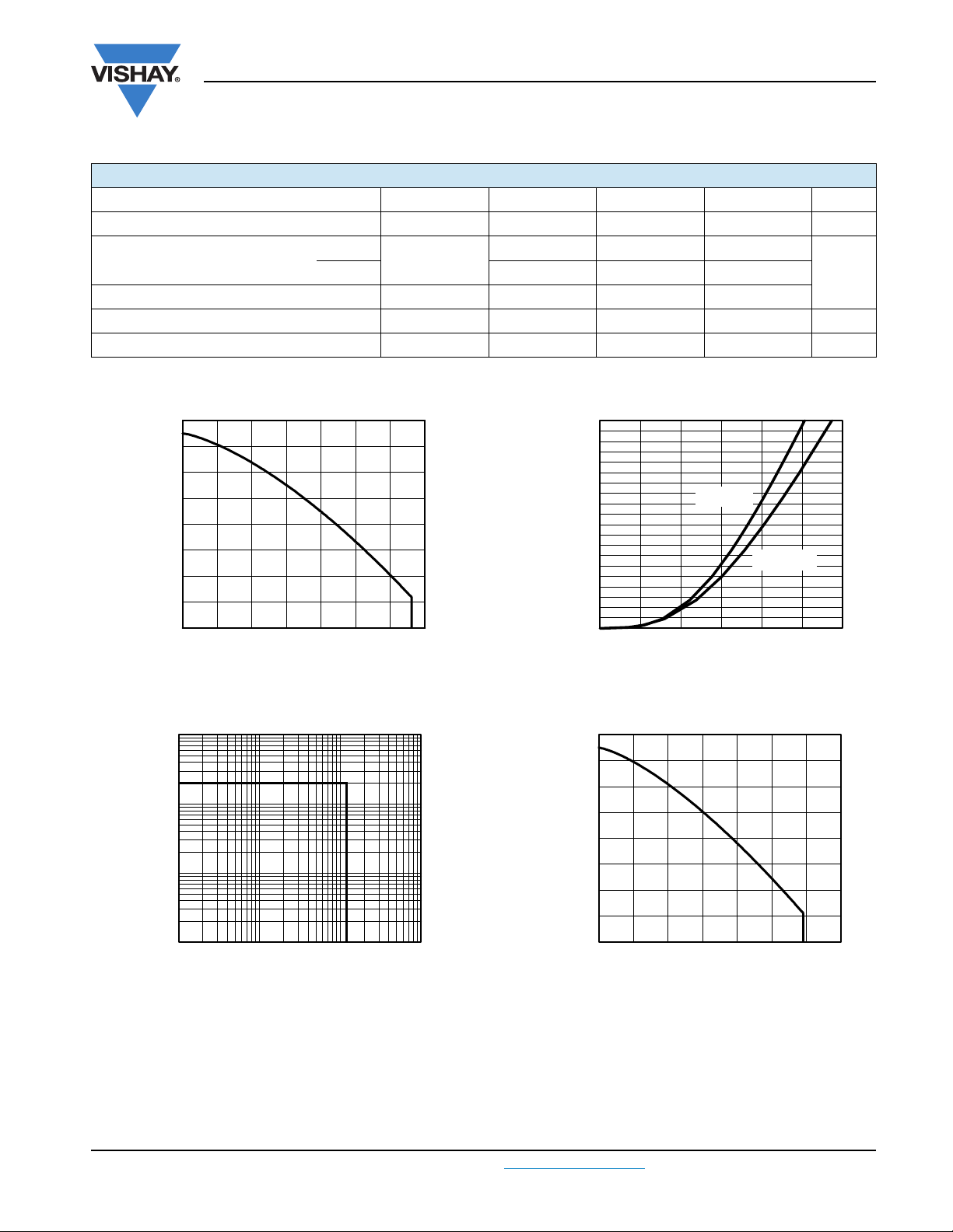
160
140
120
100
80
60
40
20
Allowable Case Temperature (°C)
0
020406080 100 120 140
IC - Continuous Collector Current (A)
Fig. 1 - Maximum DC IGBT Collector Current vs.
Case Temperature
- 40 - 150 °C
- - 0.19
°C/WDiode - - 0.52
-0.05-
200
150
TJ = 25 °C
100
(A)
C
I
TJ = 125 °C
50
0
0246135
VCE (V)
Fig. 3 - Typical IGBT Collector Current Characteristics
160
140
120
100
80
60
40
20
Allowable Case Temperature (°C)
0
0 10203040506070
IF - Continuous Forward Current (A)
Fig. 4 - Maximum DC Forward Current vs.
Case Temperature
(A)
C
I
1000
100
10
1
10 100 1000 10 000
VCE (V)
Fig. 2 - IGBT Reverse Bias SOA
T
= 150 °C, VGE = 15 V
J
Document Number: 93011 For technical questions, contact: ind-modules@vishay.com
www.vishay.com
Revision: 23-Apr-09 3
Page 5

GB75DA120UP
Vishay High Power Products
200
150
100
(A)
F
I
50
0
01 3245
Fig. 5 - Typical Diode Forward Characteristics
10
1
0.1
(mA)
CES
0.01
I
0.001
0.0001
0 200 400 600 800 1000 1200
Fig. 6 - Typical IGBT Zero Gate Voltage Collector Current
TJ = 125 °C
TJ = 125 °C
VFM (V)
V
CES
TJ = 25 °C
TJ = 25 °C
(V)
Insulated Gate Bipolar Transistor
(Ultrafast IGBT), 75 A
4.5
4.0
3.5
(V)
CE
V
3.0
2.5
2.0
25 50 75 125100 150
Fig. 8 - Typical IGBT Collector to Emitter Voltage vs.
4.0
3.5
3.0
2.5
2.0
1.5
Energy (mJ)
1.0
0.5
Junction Temperature, V
0
10 20 30 50 60 7040 80
Fig. 9 - Typical IGBT Energy Loss vs. I
TJ = 125 °C, L = 500 µH, VCC = 600 V,
100 A
75 A
27 A
TJ (°C)
E
off
IC (A)
R
= 5 Ω, VGE = 15 V
g
E
GE
on
= 15 V
C
(V)
geth
V
6.0
5.5
5.0
4.5
4.0
TJ = 25 °C
TJ = 125 °C
1000
100
t
d(off)
t
d(on)
t
f
t
r
Switching Time (µs)
3.5
3.0
0.0002 0.0004 0.0006 0.0008 0.001
IC (mA)
Fig. 7 - Typical IGBT Threshold Voltage
10
020 6040 80
IC (A)
Fig. 10 - Typical IGBT Switching Time vs. I
TJ = 125 °C, L = 500 µH, VCC = 600 V,
R
= 5 Ω, VGE = 15 V
g
C
www.vishay.com For technical questions, contact: ind-modules@vishay.com
Document Number: 93011
4 Revision: 23-Apr-09
Page 6

GB75DA120UP
14
12
10
8
6
Energy (mJ)
4
2
0
0 1020304050
Fig. 11 - Typical IGBT Energy Loss vs. R
TJ = 125 °C, IC = 75 A, L = 500 µH,
10 000
1000
100
Switching Time (µs)
10
0203010 40 50
Fig. 12 - Typical IGBT Switching Time vs. R
TJ = 125 °C, L = 500 µH, VCC = 600 V,
Insulated Gate Bipolar Transistor
RG (Ω)
V
= 600 V, VGE = 15 V
CC
t
f
t
r
RG (Ω)
R
= 5 Ω, VGE = 15 V
g
(Ultrafast IGBT), 75 A
E
on
E
off
g
t
d(on)
t
d(off)
g
Vishay High Power Products
250
230
210
190
170
(ns)
rr
150
t
130
110
90
70
100 1000
Fig. 13 - Typical t
40
35
30
25
20
(A)
rr
I
15
10
5
0
100 1000
Fig. 14 - Typical I
V
RR
TJ = 125 °C
TJ = 25 °C
dIF/dt (A/µs)
diode vs. dIF/dt
V
RR
rr
= 200 V, IF = 50 A
TJ = 125 °C
dIF/dt (A/µs)
diode vs. dIF/dt
rr
= 200 V, IF = 50 A
TJ = 25 °C
1
0.1
0.01
- Thermal Impedance
0.001
thJC
Junction to Case (°C/W)
Z
0.0001
0.00001 0.0001 0.001 0.01 0.1
(thermal response)
Single pulse
D = 0.50
D = 0.20
D = 0.10
D = 0.05
D = 0.02
D = 0.01
1
Rectangular Pulse Duration (t1)
Fig. 15 - Maximum Thermal Impedance Z
Characteristics (IGBT)
thJC
Document Number: 93011 For technical questions, contact: ind-modules@vishay.com
www.vishay.com
Revision: 23-Apr-09 5
Page 7

GB75DA120UP
r
Vishay High Power Products
1
0.1
0.01
- Thermal Impedance
thJC
Junction to Case (°C/W)
Z
0.001
0.00001 0.0001 0.001 0.01 0.1
50 V
* Dri
ver same type as D.U.T.; V
* Note: Due to the 50 V power supply, pulse width and inducto
will increase to obtain Id
1000 V
1
Single pulse
(thermal response)
Fig. 16 - Maximum Thermal Impedance Z
L
V
*
C
= 80 % of V
C
Insulated Gate Bipolar Transistor
(Ultrafast IGBT), 75 A
D = 0.50
D = 0.20
D = 0.10
D = 0.05
D = 0.02
D = 0.01
Rectangular Pulse Duration (t1)
Characteristics (diode)
thJC
D.U.T.
2
ce(max)
1
V
CC
R =
I
CM
+
-
D.U.T.
R
g
V
CC
Fig. 17a - Clamped Inductive Load Test Circuit Fig. 17b - Pulsed Collector Current Test Circuit
Diode clamp/
D.U.T.
-
- 5 V
+
R
g
L
D.U.T./
driver
+
-
V
CC
Fig. 18a - Switching Loss Test Circuit
www.vishay.com For technical questions, contact: ind-modules@vishay.com
Document Number: 93011
6 Revision: 23-Apr-09
Page 8

ORDERING INFORMATION TABLE
SOT-227 Package Details
Dimensions are shown in millimeters ( inches )
GB75DA120UP
Vishay Semiconductor Italy
4.40 (.173 )
4.20 (.165 )
12.50 ( .492 )
7.50 ( .295 )
2.10 ( .082 )
1.90 ( .075 )
4
1
38.30 ( 1.508 )
37.80 ( 1.488 )
-A-
30.20 ( 1.189 )
29.80 ( 1.173 )
4X
3
2
8.10 ( .319 )
7.70 ( .303 )
CHAMFER
2.00 ( .079 ) X 457
6.25 ( .246 )
15.00 ( .5 90 )
2.10 ( .0 82 )
1.90 ( .0 75 )
25.70 ( 1.012 )
25.20 ( .992 )
-B-
4
1
R FULL
0.25 ( .010 ) M C A M B M
-C-
0.12 ( .005 )
LEAD ASSIGMENTS
C
E
G
E
IGBT
A1
K2
3
2
K1 A2
HEXFRED
S
E
4
1
E
HEXFET
IGBT
12.30 ( .484 )
11.80 ( .464 )
D
C
3
2
GS
G
Tube
QUANTITIES PER TUBE IS 10
M4 SREW AND WASHER INCLUDED
Revision 31-Mar-08
3
Page 9

GB75DA120UP
Insulated Gate Bipolar Transistor
(Ultrafast IGBT), 75 A
1
2
3
V
C
90 %
10 %
5 %
I
C
t
d(on)
Fig. 18b - Switching Loss Waveforms Test Circuit
10 %
t
r
E
on
Ets = (Eon + E
90 %
t
d(off)
Vishay High Power Products
t
f
E
off
)
off
t = 5 µs
ORDERING INFORMATION TABLE
Device code
G B 75 D A 120 U P
1 - Insulated Gate Bipolar Transistor (IGBT)
2 - B = IGBT Generation 5
3 - Current rating (75 = 75 A)
4 - Circuit configuration (D = Single switch with antiparallel diode)
5 - Package indicator (A = SOT-227)
6 - Voltage rating (120 = 1200 V)
7 - Speed/type (U = Ultrafast IGBT)
8 - Totally lead (Pb)-free
51324678
Document Number: 93011 For technical questions, contact: ind-modules@vishay.com
www.vishay.com
Revision: 23-Apr-09 7
Page 10

GB75DA120UP
Vishay High Power Products
Insulated Gate Bipolar Transistor
(Ultrafast IGBT), 75 A
CIRCUIT CONFIGURATION
3 (C)
2 (G)
1, 4 (E)
LINKS TO RELATED DOCUMENTS
Dimensions http://www.vishay.com/doc?95036
Packaging information http://www.vishay.com/doc?95037
www.vishay.com For technical questions, contact: ind-modules@vishay.com
8 Revision: 23-Apr-09
Document Number: 93011
Page 11

Legal Disclaimer Notice
Vishay
Disclaimer
All product specifications and data are subject to change without notice.
Vishay Intertechnology, Inc., its affiliates, agents, and employees, and all persons acting on its or their behalf
(collectively, “Vishay”), disclaim any and all liability for any errors, inaccuracies or incompleteness contained herein
or in any other disclosure relating to any product.
Vishay disclaims any and all liability arising out of the use or application of any product described herein or of any
information provided herein to the maximum extent permitted by law. The product specifications do not expand or
otherwise modify Vishay’s terms and conditions of purchase, including but not limited to the warranty expressed
therein, which apply to these products.
No license, express or implied, by estoppel or otherwise, to any intellectual property rights is granted by this
document or by any conduct of Vishay.
The products shown herein are not designed for use in medical, life-saving, or life-sustaining applications unless
otherwise expressly indicated. Customers using or selling Vishay products not expressly indicated for use in such
applications do so entirely at their own risk and agree to fully indemnify Vishay for any damages arising or resulting
from such use or sale. Please contact authorized Vishay personnel to obtain written terms and conditions regarding
products designed for such applications.
Product names and markings noted herein may be trademarks of their respective owners.
Document Number: 91000 www.vishay.com
Revision: 18-Jul-08 1
 Loading...