

Page 1

6121 Baker Road,
Suite 108
Minnetonka, MN 55345
www.chtechnology.com
Phone (952) 933-6190
Fax (952) 933-6223
1-800-274-4284
Thank you for downloading this document from C&H Technology, Inc.
Please contact the C&H Technology team for the following questions -
Technical
Application
Assembly
Availability
Pricing
Phone – 1-800-274-4284
E-Mail – sales@chtechnology.com
www.chtechnology.com - SPECIALISTS IN POWER ELECTRONIC COMPONENTS AND ASSEMBLIES - www.chtechnology.com
Page 2
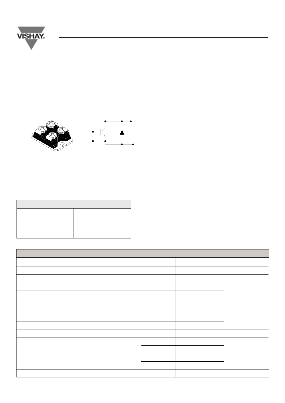
GB100DA60UP
Vishay Semiconductor Italy
IINSULATED GATE BIPOLAR TRANSISTOR
Warp2 Speed IGBT
FEATURES
• NPT Warp2 Speed IGBT Technology
with Positive Temperature Coefficient
• Hexfred Antiparallel Diodes with UltraSoft
Reverse Recovery
• Fully isolated package (2,500 volt AC)
• Very low internal inductance (5 nH typ.)
• Industry standard outline
• TOTALLY LEAD-FREE
SOT-227
PRODUCT SUMMARY
V
CES
V
CE(on) typ
I
C(DC)
I
F(DC)
2.4V @ 100A, 25°C
600V
100A @ 61°C
100A @ 85°C
ABSOLUTE MAXIMUM RATINGS
PARAMETERS MAX UNITS
V
I
I
I
I
I
V
P
CES
C
CM
LM
F
FM
GE
D
Collector-to-Emitter Voltage 600 V
Continuos Collector Current @ TC = 25°C 125 A
Pulsed Collector Current 300
Clamped Inductive Load Current 300
Diode Continuos Forward Current @ TC = 25°C 160
Peak Diode Forward Current 200
Gate-to-Emitter Voltage ± 20 V
Maximum Power Dissipation, IGBT @ TC = 25°C 447 W
BENEFITS
• Designed for increased operating efficiency in
power conversion: UPS, SMPS, Welding,
Induction heating
• Easy to assemble and parallel
• Direct mounting to heatsink
• Plug-in compatible with other SOT-227
packages
• Higher Switching Frequency up to 150kHz
• Lower Conduction Losses and Switching Losses
• Low EMI, requires Less Snubbing
@ TC = 80°C 85
@ TC = 80°C 105
@ TC = 80°C 250
P
D
V
ISOL
28-Mar-08
Maximum Power Dissipation, Diode @ TC = 25°C 313 W
@ TC = 80°C 175
Isolation Voltage, Any Terminal to Case, t = 1 min 2500 V
1
Page 3

GB100DA60UP
Vishay Semiconductor Italy
ELECTRICAL CHARACTERISTICS @ TJ = 25°C (unless otherwise specified)
PARAMETERS MIN TYP MAX UNITS TEST CONDITIONS
V
(BR)CES
V
CE(on)
V
GE(th)
I
CES
Collector-to-Emitter Breakdown Voltage 60 0 V VGE = 0V, IC = 500μA
Collector-to-Emitter Voltage 2.4 VGE = 15V, IC = 100A
3V
= 15V, IC = 100A, TJ = 125°C
GE
Gate Threshold Voltage 4 IC = 0.5mA
Collector-to-Emiter Leaking 7 μAVGE = 0V, VCE = 600V
Current 4 mA VGE = 0V, VCE = 600V, TJ = 150°C
I
GES
Gate-to-Emitter Leakage Current ± 2 00 nA VGE = ± 20V
SWITCHING CHARACTERISTICS @ TJ = 25°C (unless otherwise specified)
PARAMETERS MIN TYP MAX UNITS TEST CONDITIONS
Q
g
Q
ge
Q
gc
E
on
E
off
E
ts
E
on
E
off
E
ts
td
on
t
r
td
off
t
f
td
on
t
r
td
off
t
f
C
ies
C
oes
C
res
RBSOA Reverse Bias Safe Operating Area full square TJ = 150°C, IC = 300A
Total Gate Charge (turn-on) 460 690 nC IC = 100A
Gate-Emitter Charge (turn-on) 160 250 VCC = 480V
Gate-Collector Charge (turn-on) 70 1 30 VGE = 15V
Turn-On Switching Loss 360 μJRG = 5 Ω
Turn-Off Switching Loss 1420 I
= 100A, VCC = 360V, VGE = 15V, L = 500μH
C
Total Switching Loss 1780 Energy losses include tail and diode reverse
recovery
Turn-On Switching Loss 520 μJRG = 5 Ω
Turn-Off Switching Loss 1600 I
= 100A, VCC = 360V, VGE = 15V, L = 500μH
C
Total Switching Loss 2120 Energy losses include tail and diode reverse
recovery,
TJ = 125°C
Turn-On Delay Time 260 ns RG = 5 Ω
Rise Time 53 I
= 100A, VCC = 360V, VGE = 15V, L = 500μH
C
Turn-Off Delay Time 248 Energy losses include tail and diode reverse
Fail Time 76 recovery
Turn-On Delay Time 264 ns RG = 5 Ω
Rise Time 54 I
= 100A, VCC = 360V, VGE = 15V, L = 500μH
C
Turn-Off Delay Time 254 Energy losses include tail and diode reverse
Fail Time 80 recovery, TJ = 125°C
Input Capacitance 8000 pF VGE = 0V
Output Capacitance 790 VCC = 30V
Reverse Transfer Capacitance 110 f = 1.0 MHz
VCC = 400V, VP = 600V
RG = 22 Ω, VGE = +15V to 0V
2 Revision 28-Mar-08
Page 4

DIODE CHARACTERISTICS @ TJ = 25°C (unless otherwise specified)
PARAMETERS MIN TY P MAX UNITS TEST CONDITIONS
GB100DA60UP
Vishay Semiconductor Italy
V
FM
Diode Forward Voltage Drop 1.6 V IC = 100A, VGE = 0V
1.7 IC = 100A, VGE = 0V, TJ = 125°C
trr Diode Reverse Recovery Time 96 ns VCC = 200V, IC = 50A
Irr Diode Peak Reverse Current 10 A dI/dt = 200A/μsec
Qrr Diode Recovery Charge 480 nC
trr Diode Reverse Recovery Time 142 ns VCC = 200V, IC = 50A
Irr Diode Peak Reverse Current 16 A dI/dt = 200A/μsec
Qrr Diode Recovery Charge 1136 nC TJ = 125°C
THERMAL-MECHANICAL SPECIFICATIONS
PARAMETERS MIN TYP MAX UNITS
T
J
T
STG
R
thCS
R
thJC
T Mounting torque, 6-32 or M3 Screw 1.3 Nm
Wt Weight 30 g
Operating Junction - 40 150 °C
Storage Temperature Range - 4 0 15 0
Case-to-Sink, Flat, Greased Surface 0.05
Junction-to-case Diode 0.4 °C/W
Igbt 0.28
Revision 28-Mar-08
3
Page 5

GB100DA60UP
Vishay Semiconductor Italy
ORDERING INFORMATION TABLE
SOT-227 Package Details
Dimensions are shown in millimeters ( inches )
4.40 (.173 )
4.20 (.165 )
12.50 ( .492 )
7.50 ( .2 95 )
2.10 ( .082 )
1.90 ( .075 )
4
1
38.30 ( 1.508 )
37.80 ( 1.488 )
-A-
30.20 ( 1.189 )
29.80 ( 1.173 )
4X
3
2
8.10 ( .319 )
7.70 ( .303 )
CHAMFER
2.00 ( .079 ) X 457
6.25 ( .246 )
15.00 ( .590 )
2.10 ( .082 )
1.90 ( .075 )
25.70 ( 1.012 )
25.20 ( .992 )
-B-
4
1
R FULL
0.25 ( .010 ) M C A M B M
-C-
0.12 ( .005 )
LEAD ASSIGMENTS
C
E
G
E
IGBT
A1
K2
3
2
K1 A2
HEXFRED
S
E C
4
1
E
HEXFET
IGBT
12.30 ( .4 84 )
11.80 ( .4 64 )
D
3
2
GS
G
Tube
QUANTITIES PER TUBE IS 10
M4 SREW AND WASHER INCLUDED
4 Revision 28-Mar-08
Page 6

ORDERING INFORMATION TABLE
Device Code
G B 100 D A 60 U P
GB100DA60UP
Vishay Semiconductor Italy
1 2 3
1 - Insulated Gate Bipolar Transistor (IGBT)
2 - B = IGBT Gen V NPT
3 - Current Rating (100 = 100A)
4 - Single Switch, with diode
5 - Package Indicator (A = SOT-227)
6 Voltage Rating (60 = 600V)
7 - Speed/ Type (U = Ultra Fast)
8 - Lead-Free
4
5
6 7 8
Revision 28-Mar-08
Data and specifications subject to change without notice.
This product has been designed for Industrial Level and Lead-Free.
Qualification Standards can be found on Vishay' s Web site.
5
 Loading...