

Page 1

6121 Baker Road,
Suite 108
Minnetonka, MN 55345
www.chtechnology.com
Phone (952) 933-6190
Fax (952) 933-6223
1-800-274-4284
Thank you for downloading this document from C&H Technology, Inc.
Please contact the C&H Technology team for the following questions -
Technical
Application
Assembly
Availability
Pricing
Phone – 1-800-274-4284
E-Mail – sales@chtechnology.com
www.chtechnology.com - SPECIALISTS IN POWER ELECTRONIC COMPONENTS AND ASSEMBLIES - www.chtechnology.com
Page 2
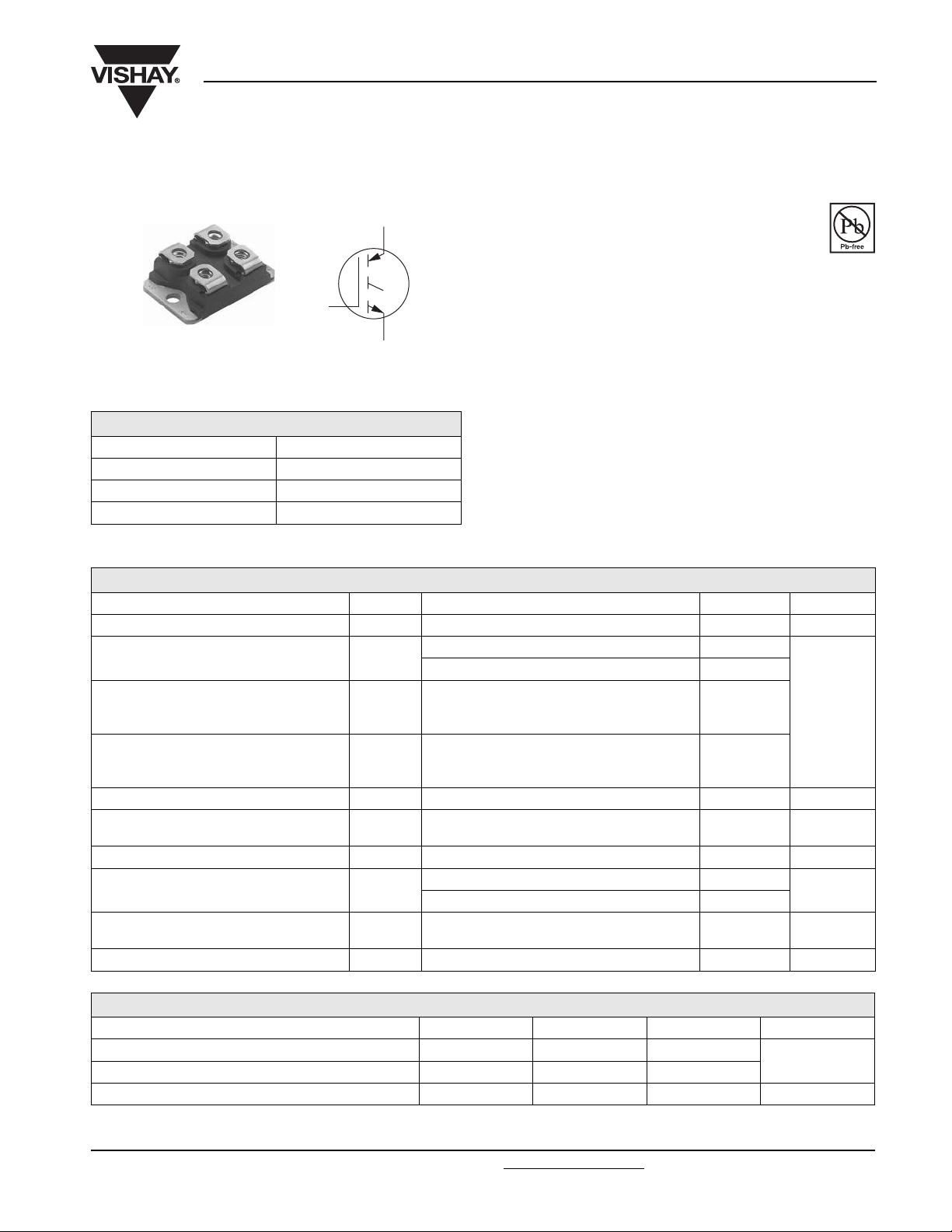
SOT-227
PRODUCT SUMMARY
V
CES
V
(typical) 1.10 V
CE(on)
V
GE
I
C
Vishay High Power Products
Insulated Gate Bipolar Transistor
(Standard Speed IGBT), 100 A
FEATURES
C
G
E
n-channel
600 V
15 V
100 A
• Standard: Optimized for minimum saturation
voltage and low operating frequencies up to 1 kHz
• Lowest conduction losses available
• Fully isolated package (2500 V
• Very low internal inductance (5 nH typical)
• Industry standard outline
• UL pending
• Completely lead (Pb)-free
• Designed and qualified for industrial level
BENEFITS
• Designed for increased operating efficiency in power
conversion: UPS, SMPS, welding, induction heating
• Easy to assemble and parallel
• Direct mounting to heatsink
• Plug-in compatible with other SOT-227 packages
GA200SA60SP
RoHS
AC
)
COMPLIANT
ABSOLUTE MAXIMUM RATINGS
PARAMETER SYMBOL TEST CONDITIONS MAX. UNITS
Collector to emitter breakdown voltage V
Continuous collector current I
Pulsed collector current I
Clamped Inductive load current I
Gate to emitter voltage V
Reverse voltage avalanche energy E
RMS isolation voltage V
Maximum power dissipation P
Operating junction and storage
temperature range
Mounting torque 6-32 or M3 screw 12 (1.3) lbf ⋅ in (N ⋅ m)
CES
C
CM
LM
GE
ARV
ISOL
T
, T
J
TC = 25 °C 200
T
= 100 °C 100
C
Repetitive rating; VGE = 20 V, pulse width limited
by maximum junction temperature
See fig. 15
VCC = 80 % (V
L = 10 µH, R
See fig. 14
Repetitive rating; pulse width limited by
maximum junction temperature
Any terminal to case, t = 1 min 2500 V
TC = 25 °C 630
D
T
= 100 °C 250
C
Stg
), VGE = 20 V,
CES
= 2.0 Ω,
G
600 V
400
400
± 20 V
155 mJ
W
- 55 to + 150 °C
A
THERMAL RESISTANCE
PARAMETER SYMBOL TYP. MAX. UNITS
Junction to case R
Case to sink, flat, greased surface R
Weight of module 30 - g
thJC
thCS
-0.20
0.05 -
°C/W
Document Number: 94363 For technical questions, contact: ind-modules@vishay.com
Revision: 29-Apr-08 1
www.vishay.com
Page 3
GA200SA60SP
Vishay High Power Products
Insulated Gate Bipolar Transistor
(Standard Speed IGBT), 100 A
ELECTRICAL CHARACTERISTICS (TJ = 25 °C unless otherwise noted)
PARAMETER SYMBOL TEST CONDITIONS MIN. TYP. MAX. UNITS
Collector to emitter breakdown voltage V
Emitter to collector breakdown voltage
Temperature coeff. of breakdown voltage ΔV
Collector to emitter saturation voltage V
Gate threshold voltage V
Temperature coeff. of threshold voltage ΔV
Forward transconductance g
Zero gate voltage collector current I
Gate to emitter leakage current I
Notes
(1)
Pulse width ≤ 80 µs; duty factor ≤ 0.1 %
(2)
Pulse width 5.0 µs, single shot
(BR)CES
V
(BR)ECS
/ΔTJVGE = 0 V, IC = 1.0 mA - 0.62 - V/°C
(BR)CES
CE(on)
GE(th)
/ΔT
GE(th)
(2)
fe
CES
GES
VGE = 0 V, IC = 250 µA 600 - -
(1)
VGE = 0 V, IC = 1.0 A 18 - -
IC = 100 A
V
= 15 V
I
= 200 A - 1.33 -
C
I
= 100 A, TJ = 150 °C - 1.02 -
C
GE
See fig. 2, 5
- 1.10 1.3
VCE = VGE, IC = 250 µA 3.0 - 6.0
VCE = VGE, IC = 2 mA - - 10 - mV/°C
J
VCE = 100 V, IC = 100 A 90 150 - S
VGE = 0 V, VCE = 600 V - - 1.0
V
= 0 V, VCE = 10 V, TJ = 150 °C - - 10
GE
VGE = ± 20 V - - ± 250 nA
V
V
mA
SWITCHING CHARACTERISTICS (TJ = 25 °C unless otherwise specified)
PARAMETER SYMBOL TEST CONDITIONS MIN. TYP. MAX. UNITS
Total gate charge (turn-on) Q
Gate collector charge (turn-on) Q
Turn-on delay time t
Rise time t
Turn-off delay time t
Fall time t
Turn-on switching loss E
Total switching loss E
Turn-on delay time t
Rise time t
Turn-off delay time t
Fall time t
Total switching loss E
Internal emitter inductance L
Input capacitance C
Reverse transfer capacitance C
ge
gc
d(on)
r
d(off)
f
on
off
ts
d(on)
r
d(off)
f
ts
E
ies
oes
res
g
IC = 100 A
= 400 V
V
CC
= 15 V; See fig. 8
V
GE
TJ = 25 °C
= 100 A
I
C
= 480 V
V
CC
= 15 V
V
GE
= 2.0 Ω
R
G
Energy losses include “tail”
See fig. 9, 10, 13
TJ = 150 °C
= 100 A, VCC = 480 V
I
C
= 15 V, RG = 2.0 Ω
V
GE
Energy losses include “tail”
See fig. 10, 11, 13
Between lead, and center of
the die contact
VGE = 0 V
V
= 30 V
CC
ƒ = 1.0 MHz; See fig. 7
- 770 1200
- 100 150
nCGate emitter charge (turn-on) Q
- 260 380
-78-
-56-
- 890 1300
ns
- 390 580
-0.98-
- 17.4 -
mJTurn-off switching loss E
- 18.4 25.5
-72-
-60-
-1500-
ns
-660-
- 35.7 - mJ
-5.0- nH
- 16 250 -
-1040-
pFOutput capacitance C
-190-
www.vishay.com For technical questions, contact: ind-modules@vishay.com
Document Number: 94363
2 Revision: 29-Apr-08
Page 4

GA200SA60SP
250
200
150
100
Load Current (A)
1000
100
50
0
0.1
TJ = 150 °C
Square wave:
60 % of rated
voltage
I
Ideal diodes
TJ = 25 °C
Insulated Gate Bipolar Transistor
(Standard Speed IGBT), 100 A
For both:
Duty cycle: 50 %
= 125 °C
T
J
= 90 °C
T
sink
Gate drive as specified
Power dissipation = 140 W
1 10 100
f - Frequency (kHz)
Fig. 1 - Typical Load Current vs. Frequency
(Load Current = I
of Fundamental)
RMS
200
150
100
Vishay High Power Products
Triangular wave:
I
Clamp voltage:
80 % of rated
10
VGE = 15 V
- Collector to Emitter Current (A)
C
I
1
0.5 1.0 1.5 2.0 2.5
20 µs pulse width
VCE - Collector to Emitter Voltage (V)
Fig. 2 - Typical Output Characteristics
1000
TJ = 150 °C
100
- Collector to Emitter Current (A)
C
I
10
567
TJ = 25 °C
VGE - Gate to Emitter Voltage (V)
Fig. 3 - Typical Transfer Characteristics
VCC = 50 V
5 µs pulse width
50
Maximum DC Collector Current (A)
0
25 50 75 100 125 150
TC - Case Temperature (°C)
Fig. 4 - Maximum Collector Current vs. Case Temperature
3
VGE = 15 V
80 µs pulse width
2
- Collector to Emitter Voltage (V)
CE
V
1
- 60 - 40 - 20 0 20 40 60 80 100 120 140 160
IC = 400 A
IC = 200 A
IC = 100 A
TJ - Junction Temperature (°C)
Fig. 5 - Typical Collector to Emitter Voltage vs.
Junction Temperature
Document Number: 94363 For technical questions, contact: ind-modules@vishay.com
www.vishay.com
Revision: 29-Apr-08 3
Page 5

GA200SA60SP
Vishay High Power Products
1
0.1
0.01
Thermal Response
-
30 000
24 000
18 000
thJC
Z
0.001
0.00001 0.0001 0.001 0.01 0.1 1
C
ies
Single pulse
(thermal resistance)
Fig. 6 - Maximum Effective Transient Thermal Impedance, Junction to Case
VGE = 0 V, f = 1 MHz
= Cge + Cgc, Cce shorted
C
ies
= C
C
res
gc
C
= Cce + C
oes
gc
Insulated Gate Bipolar Transistor
(Standard Speed IGBT), 100 A
D = 0.50
D = 0.20
D = 0.10
D = 0.05
D = 0.02
D = 0.01
t1 - Rectangular Pulse Duration (s)
25
24
23
22
VCC = 480 V
V
T
I
C
Notes:
1. Duty factor D = t
2. Peak TJ = PDM x Z
GE
= 25 °C
J
= 200 A
= 15 V
P
DM
t
1
t
2
1/t2
+ T
thJC
C
C
12 000
C - Capacitance (pF)
6000
0
1 10 100
oes
C
res
VCE - Collector to Emitter Voltage (V)
Fig. 7 - Typical Capacitance vs.
Collector to Emitter Voltage
20
VCC = 400 V
= 100 A
I
C
16
12
8
4
- Gate to Emitter Voltage (V)
GE
V
0
0 200 400 600 800
QG - Total Gate Charge (nC)
Fig. 8 - Typical Gate Charge vs. Gate to Emitter Voltage
21
20
19
Total Switching Losses (mJ)
18
01020304050
RG - Gate Resistance (Ω)
Fig. 9 - Typical Switching Losses vs. Gate Resistance
1000
RG = 2.0 Ω
= 15 V
V
GE
= 480 V
V
CC
IC = 350 A
100
IC = 200 A
IC = 100 A
Total Switching Losses (mJ)
10
- 60 - 40 - 20 0 20 40 60 80 100 120 140 160
TJ - Junction Temperature (°C)
Fig. 10 - Typical Switching Losses vs.
Junction Temperature
www.vishay.com For technical questions, contact: ind-modules@vishay.com
Document Number: 94363
4 Revision: 29-Apr-08
Page 6

GA200SA60SP
Insulated Gate Bipolar Transistor
(Standard Speed IGBT), 100 A
160
RG = 2.0 Ω
= 150 °C
T
J
= 480 V
V
120
Total Switching Losses (mJ)
Fig. 11 - Typical Switching Losses vs. Collector Current
50 V
CC
= 15 V
V
GE
80
40
0
100 150 200 250 300 350
IC - Collector Current (A)
L
V
*
C
1000 V
121
D.U.T.
Vishay High Power Products
1000
VGE = 20 V
= 125 °C
T
100
10
- Collector Current (A)
C
I
0 - 480 V
2
J
Safe operating area
1
1 10 100 1000
VCE - Collector to Emitter Voltage (V)
Fig. 14 - Turn-Off SOA
4 x I
480 V
C
480 µF
960 V
RL ==
at 25 °C
* Driver same type as D.U.T.; V
Note: Due to the 50 V power supply, pulse width and inductor
will increase to obtain rated I
= 80 % of VCE (max)
C
d
Fig. 13a - Clamped Inductive Load Test Circuit
50 V
1000 V
1
* Driver same type as D.U.T., VC = 480 V
Fig. 14a - Switching Lost Test Circuit
Driver*
2
Fig. 13b - Pulsed Collector Current Test Circuit
I
C
L
V
C
D.U.T.
3
Document Number: 94363 For technical questions, contact: ind-modules@vishay.com
www.vishay.com
Revision: 29-Apr-08 5
Page 7

GA200SA60SP
Vishay High Power Products
1
2
3
V
C
90 %
10 %
5 %
I
C
Insulated Gate Bipolar Transistor
(Standard Speed IGBT), 100 A
90 %
10 %
t
d (off)
t
t
d (on)
r
E
on
Ets = (Eon + E
Fig. 14b - Switching Loss Waveforms
t
f
E
off
)
off
t = 5 µs
ORDERING INFORMATION TABLE
Device code
Dimensions http://www.vishay.com/doc?95036
Packaging information http://www.vishay.com/doc?95037
G A 200 S A 60 S P
51324678
1 - Insulated Gate Bipolar Transistor (IGBT)
2 - Generation 4, IGBT silicon, DBC construction
3 - Current rating (200 = 200 A)
4 - Single switch, no diode
5 - SOT-227
6 - Voltage rating (60 = 600 V)
7 - Speed/type (S = Standard speed)
8 - None = Standard production
P = Lead (Pb)-free
LINKS TO RELATED DOCUMENTS
www.vishay.com For technical questions, contact: ind-modules@vishay.com
Document Number: 94363
6 Revision: 29-Apr-08
Page 8

Legal Disclaimer Notice
Vishay
Disclaimer
All product specifications and data are subject to change without notice.
Vishay Intertechnology, Inc., its affiliates, agents, and employees, and all persons acting on its or their behalf
(collectively, “Vishay”), disclaim any and all liability for any errors, inaccuracies or incompleteness contained herein
or in any other disclosure relating to any product.
Vishay disclaims any and all liability arising out of the use or application of any product described herein or of any
information provided herein to the maximum extent permitted by law. The product specifications do not expand or
otherwise modify Vishay’s terms and conditions of purchase, including but not limited to the warranty expressed
therein, which apply to these products.
No license, express or implied, by estoppel or otherwise, to any intellectual property rights is granted by this
document or by any conduct of Vishay.
The products shown herein are not designed for use in medical, life-saving, or life-sustaining applications unless
otherwise expressly indicated. Customers using or selling Vishay products not expressly indicated for use in such
applications do so entirely at their own risk and agree to fully indemnify Vishay for any damages arising or resulting
from such use or sale. Please contact authorized Vishay personnel to obtain written terms and conditions regarding
products designed for such applications.
Product names and markings noted herein may be trademarks of their respective owners.
Document Number: 91000 www.vishay.com
Revision: 18-Jul-08 1
 Loading...