

Page 1

6121 Baker Road,
Suite 108
Minnetonka, MN 55345
www.chtechnology.com
Phone (952) 933-6190
Fax (952) 933-6223
1-800-274-4284
Thank you for downloading this document from C&H Technology, Inc.
Please contact the C&H Technology team for the following questions -
Technical
Application
Assembly
Availability
Pricing
Phone – 1-800-274-4284
E-Mail – sales@chtechnology.com
www.chtechnology.com - SPECIALISTS IN POWER ELECTRONIC COMPONENTS AND ASSEMBLIES - www.chtechnology.com
Page 2
Vishay High Power Products
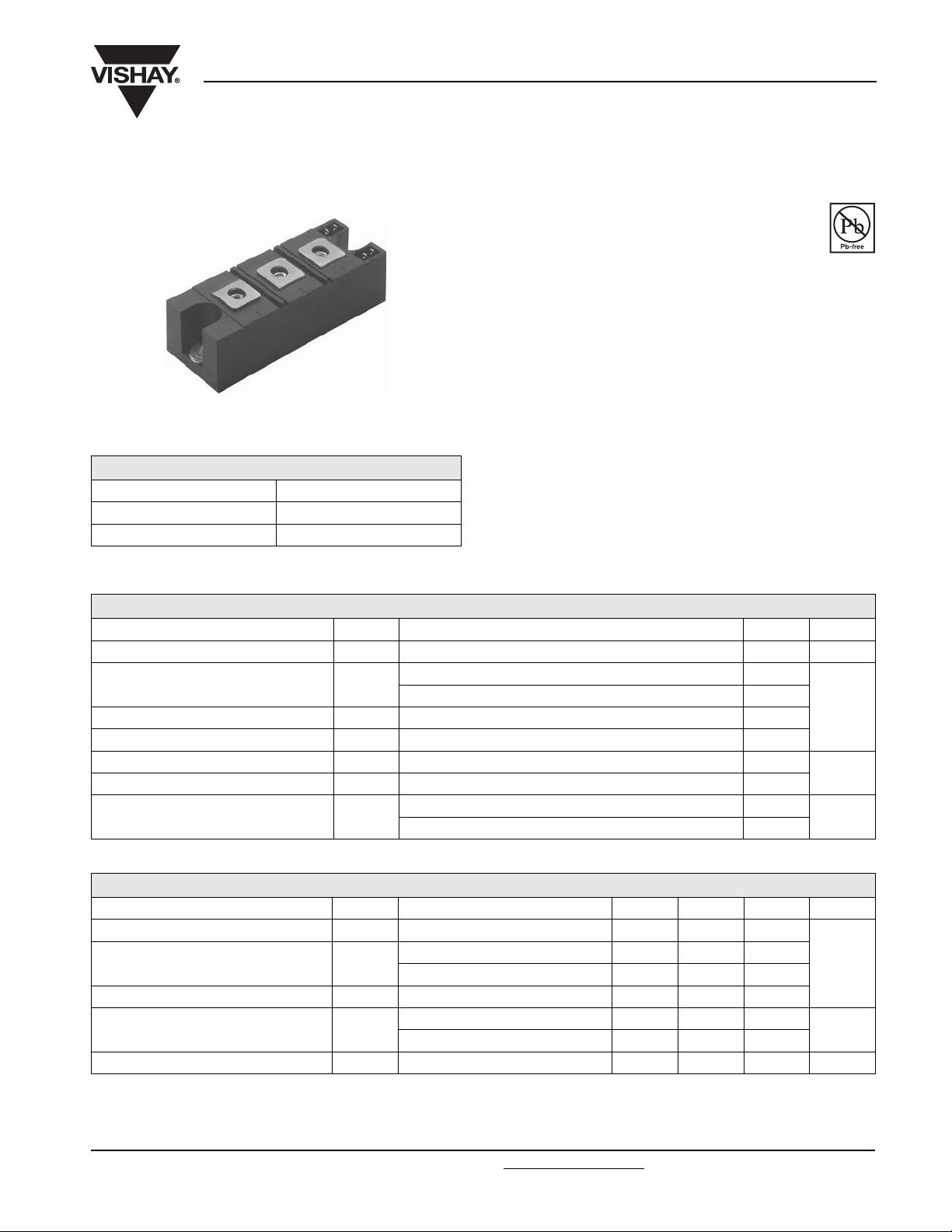
"Half-Bridge" IGBT INT-A-PAK
(Standard Speed IGBT), 200 A
FEATURES
• Generation 4 IGBT technology
GA200HS60S1PbF
• Standard speed: Optimized for hard switching
operating frequencies DC to 1 kHz
RoHS
COMPLIANT
• Very low conduction losses
• Industry standard package
• Completely lead (Pb)-free
• Designed and qualified for industrial level
INT-A-PAK
BENEFITS
PRODUCT SUMMARY
V
CES
I
DC 480 A
C
V
at 200 A, 25 °C 1.13 V
CE(on)
600 V
• Increased operating efficiency
• Direct mounting to heatsink
• Performance optimized as output inverter stage for TIG
welding machines
ABSOLUTE MAXIMUM RATINGS
PARAMETER SYMBOL TEST CONDITIONS MAX. UNITS
Collector to emitter voltage V
Continuous collector current I
Pulsed collector current I
Peak switching current I
Gate to emitter voltage V
RMS isolation voltage V
Maximum power dissipation P
CES
C
CM
LM
GE
ISOL
D
TC = 25 °C 480
= 116 °C 200
T
C
Any terminal to case, t = 1 min 2500
TC = 25 °C 830
T
= 85 °C 430
C
600 V
800
800
± 20
A
V
W
ELECTRICAL SPECIFICATIONS (TJ = 25 °C unless otherwise specified)
PARAMETER SYMBOL TEST CONDITIONS MIN. TYP. MAX. UNITS
Collector to emitter breakdown voltage V
Gate threshold voltage V
Collector to emitter leakage current I
Gate to emitter leakage current I
Document Number: 94362 For technical questions, contact: ind-modules@vishay.com
Revision: 29-Apr-08 1
BR(CES)VGE
CE(on)
GE(th)IC
CES
GES
= 0 V, IC = 1 mA 600 - -
VGE = 15 V, IC = 200 A - 1.13 1.21
V
= 15 V, IC = 200 A, TJ = 125 °C - 1.08 1.18
GE
= 0.25 mA 3 4.5 6
VGE = 0 V, VCE = 600 V - 0.025 1
V
= 0 V, VCE = 600 V, TJ = 125 °C - - 10
GE
VGE = ± 20 V - - ± 250 nA
www.vishay.com
mA
VCollector to emitter voltage V
Page 3

GA200HS60S1PbF
Vishay High Power Products
"Half-Bridge" IGBT INT-A-PAK
(Standard Speed IGBT), 200 A
SWITCHING CHARACTERISTICS (TJ = 25 °C unless otherwise specified)
PARAMETER SYMBOL TEST CONDITIONS MIN. TYP. MAX. UNITS
Total gate charge Q
Gate to collector charge Q
Turn-on switching loss E
Total switching loss E
Turn-on switching loss E
Total switching loss E
Input capacitance C
Reverse transfer capacitance C
g
ge
gc
on
off
ts
on
off
ts
ies
oes
res
IC = 200 A
= 400 V
V
CC
= 15 V
V
GE
IC = 200 A, VCC = 480 V, VGE = 15 V
= 10 Ω
R
G
Freewheeling diode: 30EPH06
IC = 200 A, VCC = 480 V, VGE = 15 V
= 10 Ω
R
G
Freewheeling diode: 30EPH06, T
= 125 °C
J
VGE = 0 V
= 30 V
V
CC
f = 1.0 MHz
THERMAL - MECHANICAL SPECIFICATIONS
PARAMETER SYMBOL MIN. TYP. MAX. UNITS
Operating junction temperature range T
Storage temperature range T
Junction to case per leg R
Case to sink R
Mounting torque
case to heatsink - - 4
case to terminal 1, 2, 3 - - 3
J
Stg
thJC
thCS
Weight - 185 - g
- 40 - 150
- 40 - 125
- - 0.15
-0.1-
- 1600 1700
- 260 340
- 580 670
-30-
-50-
-80-
-34-
-104-
- 138 151
- 32 500 -
-2080-
-380-
nCGate to emitter charge Q
mJTurn-off switching loss E
mJTurn-off switching loss E
pFOutput capacitance C
°C
°C/W
Nm
1000
VGE = 15 V
500 µs pulse width
TJ = 125 °C
100
TJ = 25 °C
- Collector to Emitter Current (A)
C
I
10
0.6
0.8
1.0
VCE - Collector to Emitter Voltage (V)
1.2 1.4
1.6
1000
100
- Collector to Emitter Current (A)
C
I
TJ = 125 °C
10
TJ = 25 °C
1
4.0
5.0 5.5 6.0 6.5 7.0 7.5
4.5
VGE - Gate to Emitter Voltage (V)
Fig. 1 - Typical Output Characteristics Fig. 2 - Typical Transfer Characteristics
www.vishay.com For technical questions, contact: ind-modules@vishay.com
Document Number: 94362
2 Revision: 29-Apr-08
Page 4

GA200HS60S1PbF
"Half-Bridge" IGBT INT-A-PAK
(Standard Speed IGBT), 200 A
160
140
120
100
80
60
40
- Case Temperature (°C)
C
T
20
0
Fig. 3 - Case Temperature vs. Maximum Collector Current
1.6
1.4
1.2
1.0
- Collector to Emitter Voltage (V)
CE
V
0.8
20 40 60 80 100 120 140
Fig. 4 - Typical Collector to Emitter Voltage vs.
100 200 300 400 500
0
Maximum DC Collector Current (A)
400 A
200 A
120 A
TJ - Junction Temperature (°C)
Junction Temperature
160
Vishay High Power Products
50
E
45
40
TJ = 25 °C
V
= 480 V
CE
= 15 V
V
GE
35
= 200 A
I
C
30
Switching Losses (mJ)
25
Freewheeling
diode 30EPH06
20
0 1020304050
RG - Gate Resistance (Ω)
Fig. 6 - Typical Switching Losses vs. Gate Resistance
80
T
= 125 °C
J
70
V
= 480 V
CE
V
= 15 V
GE
60
50
40
30
20
Switching Losses (mJ)
10
0
= 10 Ω
V
GE
Freewheeling
diode 30EPH06
50 75 100 175 200125 150
IC - Collector to Emitter Current (A)
Fig. 7 - Typical Switching Losses vs.
Collector to Emitter Current
typical
off
Eon typical
E
off
Eon typical
typical
- Gate to Emitter Voltage (V)
GE
V
16
14
12
10
8
6
4
2
0
0 300 600
Typical value
1200
900
1500
QG - Total Gate Charge (nC)
1800
6, 7
4, 5
Functional Diagram
3
6
7
1
4
5
2
3
1
2
Electrical Diagram
Fig. 5 - Typical Gate Charge vs. Gate to Emitter Voltage
Document Number: 94362 For technical questions, contact: ind-modules@vishay.com
www.vishay.com
Revision: 29-Apr-08 3
Page 5

GA200HS60S1PbF
Vishay High Power Products
ORDERING INFORMATION TABLE
Device code
GA 200 H S 60 S 1 PbF
1 - Essential part number IGBT modules
2 - Current rating (200 = 200 A)
3 - Circuit configuration (H = Half bridge without f/w diode)
4 - INT-A-PAK
5 - Voltage code (60 = 600 V)
6 - Speed/type (S = Standard speed IGBT)
7 - Assy location Italy
8 - PbF = Lead (Pb)-free
"Half-Bridge" IGBT INT-A-PAK
(Standard Speed IGBT), 200 A
51324678
LINKS TO RELATED DOCUMENTS
Dimensions http://www.vishay.com/doc?95067
www.vishay.com For technical questions, contact: ind-modules@vishay.com
4 Revision: 29-Apr-08
Document Number: 94362
Page 6

Legal Disclaimer Notice
Vishay
Disclaimer
All product specifications and data are subject to change without notice.
Vishay Intertechnology, Inc., its affiliates, agents, and employees, and all persons acting on its or their behalf
(collectively, “Vishay”), disclaim any and all liability for any errors, inaccuracies or incompleteness contained herein
or in any other disclosure relating to any product.
Vishay disclaims any and all liability arising out of the use or application of any product described herein or of any
information provided herein to the maximum extent permitted by law. The product specifications do not expand or
otherwise modify Vishay’s terms and conditions of purchase, including but not limited to the warranty expressed
therein, which apply to these products.
No license, express or implied, by estoppel or otherwise, to any intellectual property rights is granted by this
document or by any conduct of Vishay.
The products shown herein are not designed for use in medical, life-saving, or life-sustaining applications unless
otherwise expressly indicated. Customers using or selling Vishay products not expressly indicated for use in such
applications do so entirely at their own risk and agree to fully indemnify Vishay for any damages arising or resulting
from such use or sale. Please contact authorized Vishay personnel to obtain written terms and conditions regarding
products designed for such applications.
Product names and markings noted herein may be trademarks of their respective owners.
Document Number: 91000 www.vishay.com
Revision: 18-Jul-08 1
 Loading...