

Page 1

6121 Baker Road,
Suite 108
Minnetonka, MN 55345
www.chtechnology.com
Phone (952) 933-6190
Fax (952) 933-6223
1-800-274-4284
Thank you for downloading this document from C&H Technology, Inc.
Please contact the C&H Technology team for the following questions -
Technical
Application
Assembly
Availability
Pricing
Phone – 1-800-274-4284
E-Mail – sales@chtechnology.com
www.chtechnology.com - SPECIALISTS IN POWER ELECTRONIC COMPONENTS AND ASSEMBLIES - www.chtechnology.com
Page 2
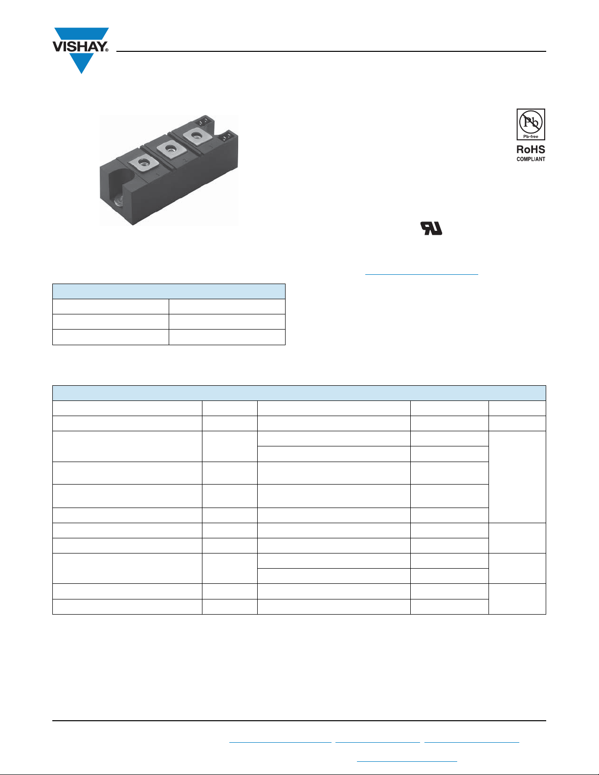
VS-GA100TS120UPbF
INT-A-PAK
www.vishay.com
Vishay Semiconductors
INT-A-PAK™ “Half-Bridge” (Ultrafast Speed IGBT), 100 A
FEATURES
• Generation 4 IGBT technology
• Ultrafast: Optimized for high speed 8 kHz to
40 kHz in hard switching, > 200 kHz in resonant
mode
• Very low conduction and switching losses
•HEXFRED
• Industry standard package
• UL approved file E78996
• Designed and qualified for industrial level
• Material categorization: For definitions of compliance
please see www.vishay.com/doc?99912
®
antiparallel diodes with ultrasoft recovery
PRODUCT SUMMARY
V
CES
DC 182 A
I
C
at 100 A, 25 °C 2.25 V
V
CE(on)
1200 V
BENEFITS
• Increased operating efficiency
• Direct mounting to heatsink
• Performance optimized for power conversion: UPS,
SMPS, welding
• Lower EMI, requires less snubbing
ABSOLUTE MAXIMUM RATINGS
PARAMETER SYMBOL TEST CONDITIONS MAX. UNITS
Collector to emitter voltage V
Continuous collector current I
Pulsed collector current I
Peak switching current
See fig. 17
Peak diode forward current I
Gate to emitter voltage V
RMS isolation voltage V
Maximum power dissipation P
Operating junction temperature range T
Storage temperature range T
CES
CM
I
LM
FM
ISOL
Stg
C
GE
TC = 25 °C 182
= 93 °C 100
T
C
Repetitive rating; VGE = 20 V, pulse width
limited by maximum junction temperature
Any terminal to case, t = 1 minute 2500
D
J
TC = 25 °C 520
T
= 85 °C 270
C
1200 V
200
200
200
± 20
- 40 to + 150
- 40 to + 125
A
V
W
°C
Revision: 26-Mar-12
For technical questions within your region: DiodesAmericas@vishay.com
THIS DOCUMENT IS SUBJECT TO CHANGE WITHOUT NOTICE. THE PRODUCTS DESCRIBED HEREIN AND THIS DOCUMENT
ARE SUBJECT TO SPECIFIC DISCLAIMERS, SET FORTH AT www.vishay.com/doc?91000
1
, DiodesAsia@vishay.com, DiodesEurope@vishay.com
Document Number: 94428
Page 3
VS-GA100TS120UPbF
www.vishay.com
ELECTRICAL SPECIFICATIONS (TJ = 25 °C unless otherwise specified)
PARAMETER SYMBOL TEST CONDITIONS MIN. TYP. MAX. UNITS
Collector to emitter breakdown voltage V
(BR)CES
VGE = 0 V, IC = 1 mA 1200 - -
VGE = 15 V, IC = 100 A - 2.25 3
Gate threshold voltage V
Temperature coefficient of threshold voltage V
GE(th)
Forward transconductance g
Collector to emitter leaking current I
Maximum diode forward voltage V
Gate to emitter leakage current I
CE(on)
GE(th)
fe
CES
FM
GES
V
= 15 V, IC = 100 A, TJ = 125 °C - 2 2.4
GE
IC = 1.25 mA 3.0 4.4 6.0
/TJVCE = VGE, IC = 1.25 mA - - 12 - mV/°C
VCE = 25 V, IC = 100 A
Pulse width 50 μs, single shot
VGE = 0 V, VCE = 1200 V - 0.03 1.0
V
= 0 V, VCE = 1200 V, TJ = 125 °C - 4.2 10
GE
VGE = 0 V, IF = 100 A - 3.3 4.0
V
= 0 V, IF = 100 A, TJ = 125 °C - 3.2 3.8
GE
VGE = ± 20 V - - 250 nA
SWITCHING CHARACTERISTICS (TJ = 25 °C unless otherwise noted)
PARAMETER SYMBOL TEST CONDITIONS MIN. TYP. MAX. UNITS
Total gate charge (turn-on) Q
Gate to collector charge (turn-on) Q
Turn-on delay time t
Rise time t
Turn-off delay time t
Fall time t
Turn-on switching energy E
Total switching energy E
Turn-on delay time t
Rise time t
Turn-off delay time t
Fall time t
Turn-on switching energy E
Total switching energy E
Input capacitance C
Reverse transfer capacitance C
Diode reverse recovery time t
Diode peak reverse current I
Diode recovery charge Q
Diode peak rate of fall of recovery during t
b
Note
(1)
Repetitive rating; VGE = 20 V, pulse width limited by maximum junction temperature
dI
d(on)
d(off)
off
ts
d(on)
d(off)
off
ts
oes
(rec)M
g
ge
gc
r
f
on
(1)
(1)
r
f
on
(1)
(1)
ies
res
rr
rr
rr
VCC = 400 V
I
= 124 A
C
Rg1 = 15
R
= 0
g2
I
= 100 A
C
= 720 V
V
CC
= ± 15 V
V
GE
T
= 25 °C
J
Rg1 = 15
= 0
R
g2
I
= 100 A
C
V
= 720 V
CC
= ± 15 V
V
GE
= 125 °C
T
J
VGE = 0 V
V
= 30 V
CC
f = 1 MHz
IC = 100 A
= 15
R
g1
R
= 0
g2
V
= 720 V
/dt - 1916 - A/μs
CC
dI/dt = 1300 A/μs
Vishay Semiconductors
- 136 - S
- 830 1245
- 140 210
- 275 412
- 570 -
-85-
- 581 -
- 276 -
-7.6-
-6.8-
- 14.4 -
- 571 -
-89-
- 606 -
- 649 -
-10-
-16-
-2645
- 18 672 -
- 830 -
- 161 -
- 149 - ns
- 104 - A
- 7664 - nC
VCollector to emitter voltage V
mA
V
nCGate to emitter charge (turn-on) Q
ns
mJTurn-off switching energy E
ns
mJTurn-off switching energy E
pFOutput capacitance C
Revision: 26-Mar-12
For technical questions within your region: DiodesAmericas@vishay.com
2
, DiodesAsia@vishay.com, DiodesEurope@vishay.com
Document Number: 94428
THIS DOCUMENT IS SUBJECT TO CHANGE WITHOUT NOTICE. THE PRODUCTS DESCRIBED HEREIN AND THIS DOCUMENT
ARE SUBJECT TO SPECIFIC DISCLAIMERS, SET FORTH AT www.vishay.com/doc?91000
Page 4
VS-GA100TS120UPbF
0.1 1 10 100
0
25
50
75
100
f - Frequency (kHz)
Load Current (A)
Duty cycle: 50 %
T
J
= 125 °C
T
sink
= 90 °C
Gate drive as specified
Power dissipation = 170 W
Ideal diodes
60 % of rated
voltage
Square wave:
-
0.5 1.0 1.5 2.0 2.5 3.0
1
10
100
1000
VGE = 15 V
500 µs pulse width
25 °C
125 °C
VCE - Collector to Emitter Voltage (V)
I
C
- Collector Current (A)
4.0 4.5 5.0 5.5 6.0 6.5 7.0 7.5
1
10
100
1000
VGE - Gate to Emitter Voltage (V)
I
C
- Collector to Emitter Current (A)
VGE = 20 V
500 µs pulse width
125 °C
25 °C
www.vishay.com
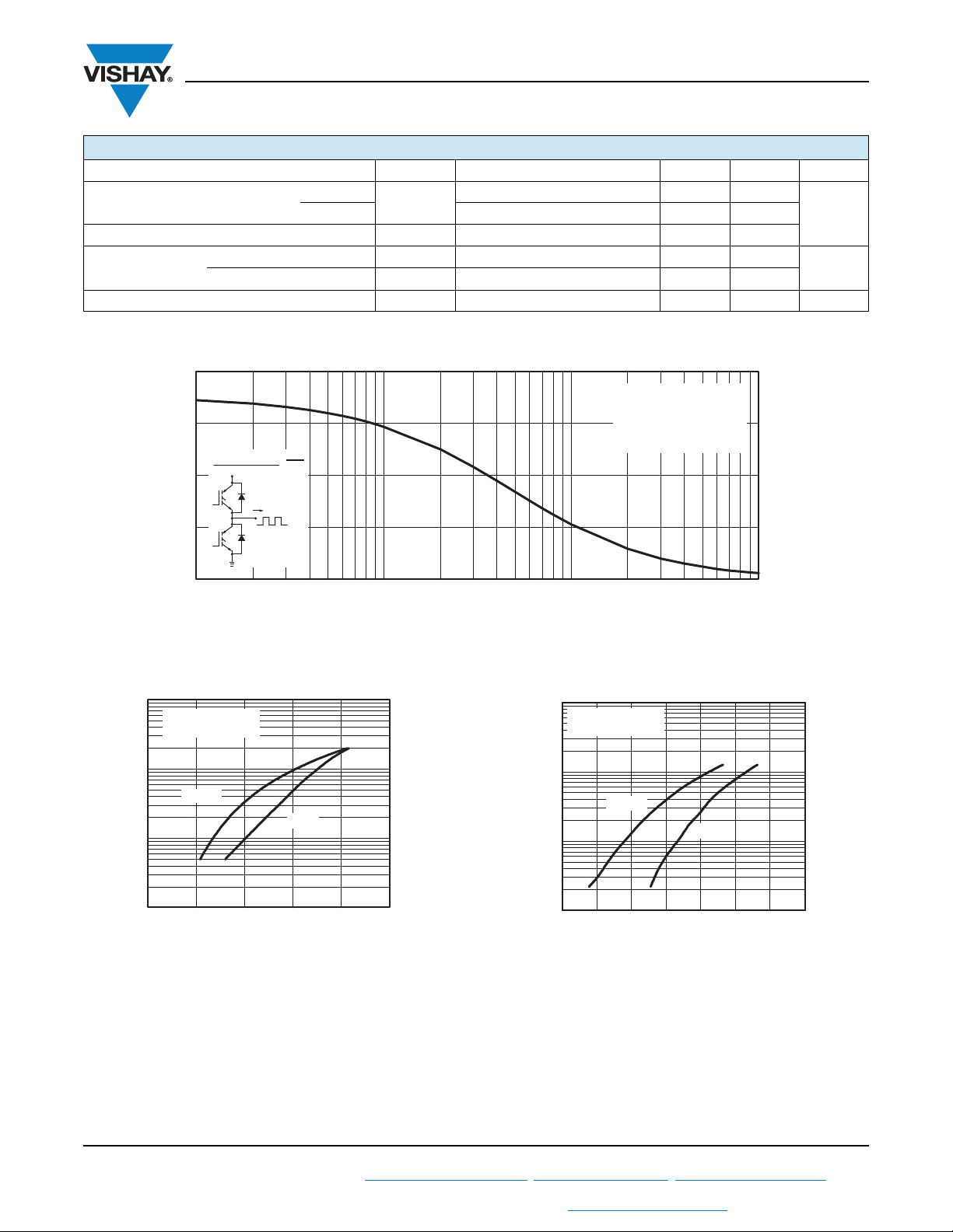
THERMAL AND MECHANICAL SPECIFICATIONS
PARAMETER SYMBOL TEST CONDITIONS TYP. MAX. UNITS
Thermal resistance, junction to case
Thermal resistance, case to sink per module R
Mounting torque
case to terminal 1, 2 and 3 For screws M5 x 0.8 - 3.0
case to heatsink - 4.0
Weight of module 200 - g
IGBT
R
thJC
thCS
Vishay Semiconductors
-0.24
°C/WDiode - 0.35
0.1 -
Nm
Fig. 1 - Typical Load Current vs. Frequency
(Load Current = I
Revision: 26-Mar-12
Fig. 2 - Typical Output Characteristics Fig. 3 - Typical Transfer Characteristics
For technical questions within your region: DiodesAmericas@vishay.com
THIS DOCUMENT IS SUBJECT TO CHANGE WITHOUT NOTICE. THE PRODUCTS DESCRIBED HEREIN AND THIS DOCUMENT
ARE SUBJECT TO SPECIFIC DISCLAIMERS, SET FORTH AT www.vishay.com/doc?91000
of Fundamental)
RMS
3
, DiodesAsia@vishay.com, DiodesEurope@vishay.com
Document Number: 94428
Page 5

www.vishay.com
0 40 80 120 160 200
0
20
40
60
80
100
120
140
160
T
C
- Case Temperature (°C)
Maximum DC Collector Current (A)
DC
0 30 60 90 120 150
1.5
2.0
2.5
3.0
VGE = 15 V
500 µs pulse width
TJ - Junction Temperature (°C)
V
CE
- Collector to Emitter Voltage (V)
IC = 50 A
IC = 200 A
IC = 100 A
0.01
0.1
1
0.0001 0.001 0.01 0.1 1
t1 - Rectangular Pulse Duration (s)
Z
thJC
- Thermal Response
10
.
P
DM
t
1
t
2
Notes:
1. Duty factor D = t
1/t2
2. Peak TJ = PDM x Z
thJC
+ T
C
Single pulse
(thermal resistance)
D = 0.50
D = 0.20
D = 0.10
D = 0.05
D = 0.02
D = 0.01
0 300 600 900
0
4
8
12
16
20
QG - Total Gate Charge (nC)
V
GE
- Gate to Emitter Voltage (V)
VCC = 400 V
I
C
= 113 A
VS-GA100TS120UPbF
Vishay Semiconductors
35 000
28 000
21 000
Fig. 4 - Case Temperature vs.
Maximum Collector Current
Fig. 6 - Maximum Effective Transient Thermal Impedance, Junction to Case
VGE = 0 V, f = 1 MHz
= Cge + Cgc, Cce shorted
C
ies
= C
C
res
gc
C
= Cce + C
C
ies
oes
gc
Fig. 5 - Typical Collector to Emitter Voltage vs.
Junction Temperature
C
14 000
C - Capacitance (pF)
7000
Revision: 26-Mar-12
THIS DOCUMENT IS SUBJECT TO CHANGE WITHOUT NOTICE. THE PRODUCTS DESCRIBED HEREIN AND THIS DOCUMENT
C
0
1 10 100
VCE - Collector to Emitter Voltage (V)
For technical questions within your region: DiodesAmericas@vishay.com
oes
res
Fig. 7 - Typical Capacitance vs.
Collector to Emitter Voltage
ARE SUBJECT TO SPECIFIC DISCLAIMERS, SET FORTH AT www.vishay.com/doc?91000
Fig. 8 - Typical Gate Charge vs. Gate to Emitter Voltage
4
, DiodesAsia@vishay.com, DiodesEurope@vishay.com
Document Number: 94428
Page 6

www.vishay.com
Total Switching Losses (mJ)
IC - Collector Current (A)
0 50 100 150 200
0
10
20
30
40
50
60
I
C
- Collector Current (A)
0
100
200
300
0 300 600 900 1200 1500
VCE - Collector to Emitter Voltage (V)
Safe operating area
VGE = 20 V
T
J
= 125 °C
V
CE
measured at terminal (peak voltage)
1
100
10
1000
0.5 1.0 1.5 2.0 2.5 3.0 3.5
VF - Forward Voltage Drop (V)
I
F
- Instantaneous Forward Current (A)
TJ = 125 °C
TJ = 25 °C
40
35
30
25
Total Switching Losses (mJ)
20
10 20 30 40 50
RG - Gate Resistance (Ω)
Fig. 9 - Typical Switching Losses vs. Gate Resistance
100
IC = 200 A
VS-GA100TS120UPbF
Vishay Semiconductors
Fig. 12 - Reverse Bias SOA
IC = 100 A
10
Total Switching Losses (mJ)
1
0 30 60 90 120 150
TJ - Junction Temperature (°C)
Fig. 10 - Typical Switching Losses vs.
Junction Temperature
Fig. 11 - Typical Switching Losses vs. Collector Current
Revision: 26-Mar-12
For technical questions within your region: DiodesAmericas@vishay.com
THIS DOCUMENT IS SUBJECT TO CHANGE WITHOUT NOTICE. THE PRODUCTS DESCRIBED HEREIN AND THIS DOCUMENT
IC = 50 A
Fig. 13 - Typical Forward Voltage Drop vs.
Instantaneous Forward Current
16 000
12 000
(nC)
rr
Q
VR = 720 V
= 125 °C
T
J
= 25 °C
T
J
8000
4000
0
400 1200 1600
800
dIF/dt (A/µs)
Fig. 14 - Typical Stored Charge vs. dI
5
, DiodesAsia@vishay.com, DiodesEurope@vishay.com
ARE SUBJECT TO SPECIFIC DISCLAIMERS, SET FORTH AT www.vishay.com/doc?91000
IF = 200 A
= 100 A
I
F
= 50 A
I
F
2000
/dt
F
Document Number: 94428
Page 7

www.vishay.com
∫
t2
t1
5 % V
CE
I
C
I
pk
V
CC
10 % I
C
V
CE
t1
t2
D.U.T. voltage
and current
Gate voltage D.U.T.
+ V
G
10 % + V
G
90 % I
C
t
r
t
d(on)
Eon =
VCE IC dt
VS-GA100TS120UPbF
Vishay Semiconductors
240
200
VR = 720 V
= 125 °C
T
J
= 25 °C
T
J
160
(ns)
rr
t
120
80
400 800 1600 2000
1200
dIF/dt (A/µs)
IF = 200 A
= 100 A
I
F
= 50 A
I
F
250
200
IF = 200 A
= 100 A
I
F
= 50 A
I
F
150
(A)
100
RRM
I
50
0
400 800 1600 2000
VR = 720 V
T
T
1200
= 125 °C
J
= 25 °C
J
dIF/dt (A/µs)
Fig. 15 - Typical Reverse Recovery Time vs. dIF/dt Fig. 16 - Typical Recovery Current vs. dIF/dt
L2
L1
+
V
CC
-
+ V
- V
G2
R
G2
R
+
G2
G1
R
G2
R
G1
L
L3
Fig. 17a - Test Circuit for Measurement of I
I
, t
rr
d(on)
90 % V
+ V
GE
V
CE
10 % V
CE
t
d(off)
t1
Defining E
ARE SUBJECT TO SPECIFIC DISCLAIMERS, SET FORTH AT www.vishay.com/doc?91000
Revision: 26-Mar-12
For technical questions within your region: DiodesAmericas@vishay.com
THIS DOCUMENT IS SUBJECT TO CHANGE WITHOUT NOTICE. THE PRODUCTS DESCRIBED HEREIN AND THIS DOCUMENT
I
C
Fig. 17b - Test Waveforms for Circuit of Fig. 18a,
V
= 60 % of BV
CC
LS = L1 + L2 + L3
= ± 15 V
V
GE
, tr, t
, t
d(off)
GE
90 % I
I
C
t
f
t2
, t
, t
off
d(off)
LM
f
E
f
, Eon, E
C
5 % I
=
off
∫
CES
off(diode)
C
t1 + 5 µs
Vce ic dt
VCE IC dt
t1
, trr, Qrr,
Fig. 17c - Test Waveforms for Circuit of Fig. 18a,
I
C
t
x
10 % V
V
pk
Diode reverse
recovery energy
I
Defining E
CC
rr
, t
, t
on
d(on)
r
t
t
rr
10 % I
Diode recovery
waveforms
E
rec
t3
t4
Qrr =
=
rr
VD IC dt
∫
t3
∫
t4
id dt
IC dt
t
x
rr
V
CC
Fig. 17d - Test Waveforms for Circuit of Fig. 18a,
Defining E
6
, trr, Qrr, I
rec
rr
Document Number: 94428
, DiodesAsia@vishay.com, DiodesEurope@vishay.com
Page 8

www.vishay.com
V
G
Gate signal
device under test
Current D.U.T.
Voltage in D.U.T.
Current in D1
t0
t1
t2
2 - Insulated gate bipolar transistor (IGBT)
1 - Vishay Semiconductors product
3 - Generation 4, IGBT silicon, DBC construction
4 - Current rating (100 = 100 A)
5 - Circuit configuration (T = Half-bridge)
6 - Package indicator (INT-A-PAK)
7 - Voltage rating (120 = 1200 V)
8 - Speed/type (U = Ultrafast)
9
- PbF = Lead (Pb)-free
Device code
51 32 4 6 7 8 9
GVS- A 100 T S 120 U PbF
VS-GA100TS120UPbF
Vishay Semiconductors
Fig. 17e - Macro Waveforms for Figure 18a‘s Test Circuit
L
1000 V
50 V
6000 µF
100 V
* Driver same type as D.U.T.; VC = 80 % of VCE (max)
Note: Due to the 50 V power supply, pulse width and inductor
will increase to obtain rated I
V
*
C
d
Fig. 18 - Clamped Inductive Load Test Circuit Fig. 19 - Pulsed Collector Current Test Circuit
ORDERING INFORMATION TABLE
D.U.T.
0 - 480 V
RL ==
4 x I
480 V
at 25 °C
C
Revision: 26-Mar-12
For technical questions within your region: DiodesAmericas@vishay.com
THIS DOCUMENT IS SUBJECT TO CHANGE WITHOUT NOTICE. THE PRODUCTS DESCRIBED HEREIN AND THIS DOCUMENT
ARE SUBJECT TO SPECIFIC DISCLAIMERS, SET FORTH AT www.vishay.com/doc?91000
7
Document Number: 94428
, DiodesAsia@vishay.com, DiodesEurope@vishay.com
Page 9

VS-GA100TS120UPbF
1
2
3
5
4
7
6
www.vishay.com
CIRCUIT CONFIGURATION
LINKS TO RELATED DOCUMENTS
Dimensions www.vishay.com/doc?95173
Vishay Semiconductors
Revision: 26-Mar-12
8
For technical questions within your region: DiodesAmericas@vishay.com
THIS DOCUMENT IS SUBJECT TO CHANGE WITHOUT NOTICE. THE PRODUCTS DESCRIBED HEREIN AND THIS DOCUMENT
ARE SUBJECT TO SPECIFIC DISCLAIMERS, SET FORTH AT www.vishay.com/doc?91000
, DiodesAsia@vishay.com, DiodesEurope@vishay.com
Document Number: 94428
Page 10

www.vishay.com
DIMENSIONS in millimeters (inches)
30
(1.18)
INT-A-PAK IGBT
9 (0.33)
7 (0.28)
28 (1.10)
Outline Dimensions
Vishay Semiconductors
29 (1.15)
14.5
35 (1.38)
3 screws M6 x 10
(0.57)
(Ø 0.25)
17 (0.67)
Ø 6.5
1
23 (0.91)
2
66 (2.60)
94 (3.70)
80 (3.15)
23 (0.91)
3
14.3
(0.56)
5 (0.20)
7
6
2.8 x 0.8
(0.11 x 0.03)
4
5
37 (1.44)
Revision: 27-Mar-13
For technical questions within your region: DiodesAmericas@vishay.com
1
, DiodesAsia@vishay.com, DiodesEurope@vishay.com
Document Number: 95173
THIS DOCUMENT IS SUBJECT TO CHANGE WITHOUT NOTICE. THE PRODUCTS DESCRIBED HEREIN AND THIS DOCUMENT
ARE SUBJECT TO SPECIFIC DISCLAIMERS, SET FORTH AT www.vishay.com/doc?91000
Page 11

Legal Disclaimer Notice
www.vishay.com
Vishay
Disclaimer
ALL PRODUCT, PRODUCT SPECIFICATIONS AND DATA ARE SUBJECT TO CHANGE WITHOUT NOTICE TO IMPROVE
RELIABILITY, FUNCTION OR DESIGN OR OTHERWISE.
Vishay Intertechnology, Inc., its affiliates, agents, and employees, and all persons acting on its or their behalf (collectively,
“Vishay”), disclaim any and all liability for any errors, inaccuracies or incompleteness contained in any datasheet or in any other
disclosure relating to any product.
Vishay makes no warranty, representation or guarantee regarding the suitability of the products for any particular purpose or
the continuing production of any product. To the maximum extent permitted by applicable law, Vishay disclaims (i) any and all
liability arising out of the application or use of any product, (ii) any and all liability, including without limitation special,
consequential or incidental damages, and (iii) any and all implied warranties, including warranties of fitness for particular
purpose, non-infringement and merchantability.
Statements regarding the suitability of products for certain types of applications are based on Vishay’s knowledge of typical
requirements that are often placed on Vishay products in generic applications. Such statements are not binding statements
about the suitability of products for a particular application. It is the customer’s responsibility to validate that a particular
product with the properties described in the product specification is suitable for use in a particular application. Parameters
provided in datasheets and/or specifications may vary in different applications and performance may vary over time. All
operating parameters, including typical parameters, must be validated for each customer application by the customer’s
technical experts. Product specifications do not expand or otherwise modify Vishay’s terms and conditions of purchase,
including but not limited to the warranty expressed therein.
Except as expressly indicated in writing, Vishay products are not designed for use in medical, life-saving, or life-sustaining
applications or for any other application in which the failure of the Vishay product could result in personal injury or death.
Customers using or selling Vishay products not expressly indicated for use in such applications do so at their own risk. Please
contact authorized Vishay personnel to obtain written terms and conditions regarding products designed for such applications.
No license, express or implied, by estoppel or otherwise, to any intellectual property rights is granted by this document or by
any conduct of Vishay. Product names and markings noted herein may be trademarks of their respective owners.
Material Category Policy
Vishay Intertechnology, Inc. hereby certifies that all its products that are identified as RoHS-Compliant fulfill the
definitions and restrictions defined under Directive 2011/65/EU of The European Parliament and of the Council
of June 8, 2011 on the restriction of the use of certain hazardous substances in electrical and electronic equipment
(EEE) - recast, unless otherwise specified as non-compliant.
Please note that some Vishay documentation may still make reference to RoHS Directive 2002/95/EC. We confirm that
all the products identified as being compliant to Directive 2002/95/EC conform to Directive 2011/65/EU.
Vishay Intertechnology, Inc. hereby certifies that all its products that are identified as Halogen-Free follow Halogen-Free
requirements as per JEDEC JS709A standards. Please note that some Vishay documentation may still make reference
to the IEC 61249-2-21 definition. We confirm that all the products identified as being compliant to IEC 61249-2-21
conform to JEDEC JS709A standards.
Revision: 02-Oct-12
1
Document Number: 91000
 Loading...