

Page 1

6121 Baker Road,
Suite 108
Minnetonka, MN 55345
www.chtechnology.com
Phone (952) 933-6190
Fax (952) 933-6223
1-800-274-4284
Thank you for downloading this document from C&H Technology, Inc.
Please contact the C&H Technology team for the following questions -
Technical
Application
Assembly
Availability
Pricing
Phone – 1-800-274-4284
E-Mail – sales@chtechnology.com
www.chtechnology.com - SPECIALISTS IN POWER ELECTRONIC COMPONENTS AND ASSEMBLIES - www.chtechnology.com
Page 2
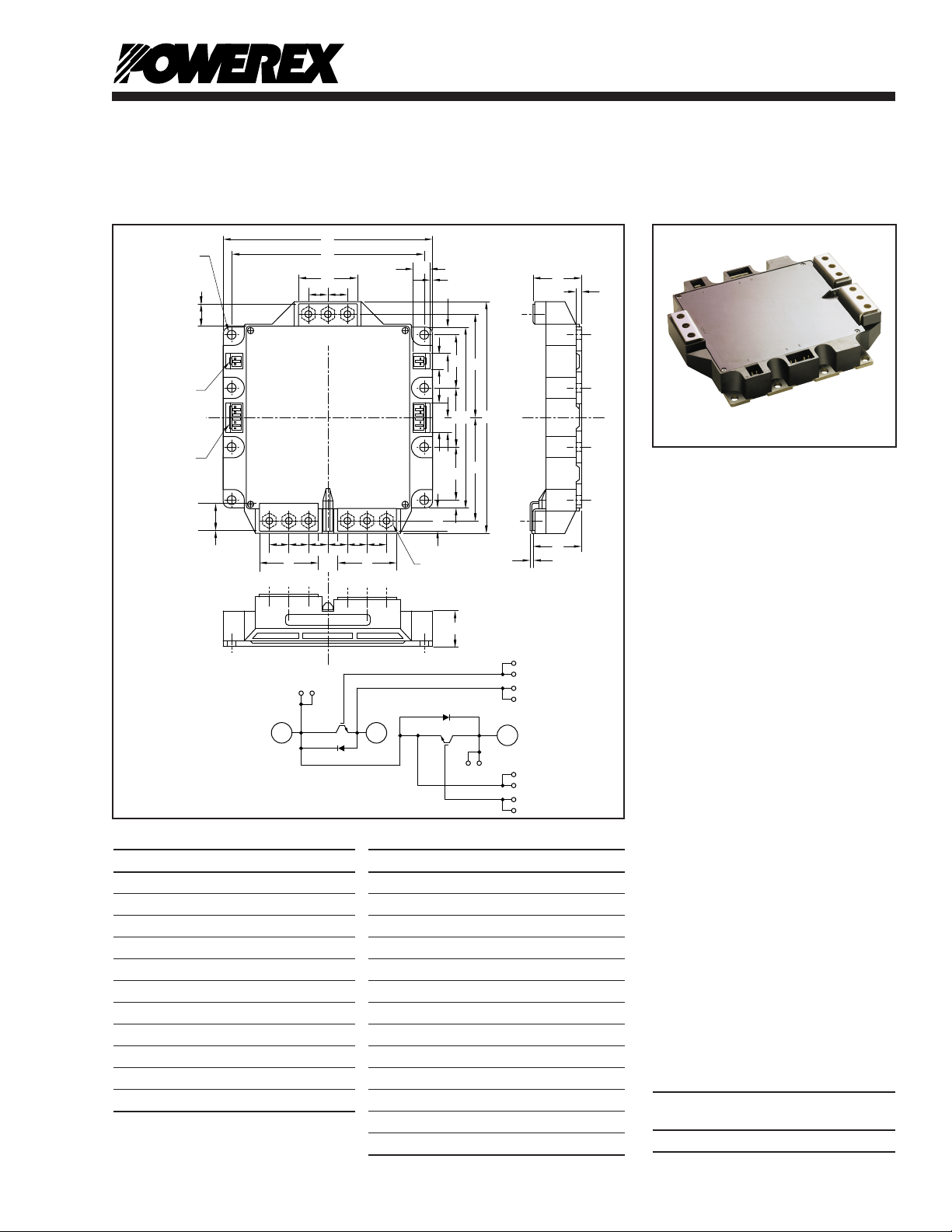
CM900DUC-24NF
A
D
P
(8 PLACES)
L
L
M
H H HHH H
K
G
U
H H
E
F
F
E2
C2
C2E1
C1
G2 E1
E2 G1
C1
V
BB
CC
B
C
J
J
G G
R (9 PLACES)
C2E1
E2
G2
E2
E1
G1
C2
Tr2
Di2
Di1
LABEL
U
W
S
N
X
Y
Z
AA
C1
C1
T
Tr1
Powerex, Inc., 173 Pavilion Lane, Youngwood, Pennsylvania 15697 (724) 925-7272
www.pwrx.com
Mega Power
Dual IGBTMOD™
900 Amperes/1200 Volts
Description:
Powerex Mega Power Dual (MPD)
Modules are designed for use in
switching applications. Each
module consists of two IGBT
Transistors having a reverseconnected super-fast recovery
free-wheel diode. All components
and interconnects are isolated
from the heat sinking baseplate,
Outline Drawing and Circuit Diagram
Dimensions Inches Millimeters
A 5.91 150.0
B 5.10 129.5
C 1.67±0.01 42.5±0.25
D 5.41±0.01 137.5±0.25
E 6.54 166.0
F 2.91±0.01 74.0±0.25
G 1.65 42.0
H 0.55 14.0
J 1.50±0.01 38.0±0.25
K 0.16 4.0
L 1.36 +0.04/-0.02 34.6 +1.0/-0.5
Housing Type (J.S.T. MFG. CO. LTD)
BB = VHR-2N
CC = VHR-5N
Dimensions Inches Millimeters
M 0.075±0.008 1.9±0.2
N 0.47 12.0
P 0.26 6.5
R M6 Metric M6
S 0.08 2.0
T 0.99 25.1
U 0.62 15.7
V 0.71 18.0
W 0.75 19.0
X 0.43 11.0
Y 0.83 21.0
Z 0.41 10.5
AA 0.22 5.5
offering simplified system assembly
and thermal management.
Features:
£ Low Drive Power
£ Low V
£
CE(sat)
Discrete Super-Fast Recovery
Free-Wheel Diode
£ Isolated Baseplate for Easy
Heatsinking
£ RoHS Compliant
Applications:
£ High Power DC Power Supply
£ Large DC Motor Drives
£ Utility Interface Inverters
Ordering Information:
Example: Select the complete
module number you desire from
the table - i.e. CM900DUC-24NF
is a 1200V (V
Dual IGBTMOD Power
Module.
Current Rating V
Type Amperes Volts (x 50)
CM 900 24
), 900 Ampere
CES
CES
101/10 Rev. 0
Page 3

Powerex, Inc., 173 Pavilion Lane, Youngwood, Pennsylvania 15697 (724) 925-7272 www.pwrx.com
CM900DUC-24NF
Mega Power Dual IGBTMOD™
900 Amperes/1200 Volts
Absolute Maximum Ratings, Tj = 25°C unless otherwise specied
Ratings Symbol CM900DUC-24NF Units
Junction Temperature Tj -40 to 150 °C
Storage Temperature T
Collector-Emitter Voltage (G-E SHORT) V
Gate-Emitter Voltage (C-E SHORT) V
Collector Current DC (TC = 96°C)*1 I
Peak Collector Current (Pulse, Tj ≤ 150°C)*4 I
Emitter Current (TC = 25°C) I
Peak Emitter Current (Pulse)*4 I
Maximum Collector Dissipation (Tj < 150°C, TC = 25°C)*1 P
Mounting Torque, M6 Mounting Screws – 40 in-lb (max.)
Mounting Torque, M6 Main Terminal Screw – 40 in-lb (max.)
Weight (Typical) – 1450 Grams
Isolation Voltage (Main Terminal to Baseplate, AC 1 min.) V
*1 Case temperatureTC and heatsink temperature (Tf) measured point is just under the chips.
*3 IE, IEM, VEC, I
*4 Pulse width and repetition rate should be such that device junction temperature (Tj) does not exceed T
, I2t, trr, Qrr represent ratings and characteristics of the anti-parallel, emitter-to-collector free-wheel diode (FWDi).
FSM
-40 to 125 °C
stg
1200 Volts
CES
±20 Volts
GES
900 Amperes
C
CM
*3
900 Amperes
E
*3
1800 Amperes
EM
5900 Watts
C
2500 Volts
iso
1800 Amperes
rating.
j(max)
2 01/10 Rev. 0
Page 4

Powerex, Inc., 173 Pavilion Lane, Youngwood, Pennsylvania 15697 (724) 925-7272 www.pwrx.com
CM900DUC-24NF
Mega Power Dual IGBTMOD™
900 Amperes/1200 Volts
Electrical Characteristics, Tj = 25°C unless otherwise specied
Characteristics Symbol Test Conditions Min. Typ. Max. Units
Collector-Cutoff Current I
Gate-Emitter Threshold Voltage V
Gate Leakage Current I
Collector-Emitter Saturation Voltage (Chip) V
CES
I
GE(th)
V
GES
IC = 900A, VGE = 15V, Tj = 25°C*6 – 1.8 2.5 Volts
CE(sat)
(Without Lead Resistance) IC = 900A, VGE = 15V, Tj = 125°C*6 – 2.0 – Volts
Module Lead Resistance R
Input Capacitance C
Output Capacitance C
Reverse Transfer Capacitance C
I
(lead)
– – 140 nF
ies
V
oes
– – 3 nF
res
Total Gate Charge QG VCC = 600V, IC = 900A, VGE = 15V – 4800 – nC
Inductive Turn-on Delay Time t
V
d(on)
Load Rise Time tr V
Switch Turn-off Delay Time t
R
d(off)
Times Fall Time tf Switching Operation – – 300 ns
Reverse Recovery Time t
Reverse Recovery Charge Q
Emitter-Collector Voltage (Chip) V
*3
I
rr
*3
– 50 – µC
rr
*3
I
EC
(Without Lead resistance)
External Gate Resistance RG 0.35 – 2.2 Ω
VCE = V
= 90mA, VCE = 10V 6 7 8 Volts
C
GE
= 900A, Terminal-Chip – 0.286 – mΩ
C
CE
CC
GE1
= 0.35Ω, Inductive Load – – 800 ns
G
= 900A, VGE = 0V*6 – – 3.2 Volts
E
, VGE = 0V – – 1 mA
CES
= V
, VCE = 0V – – 1.0 µA
GES
= 10V, VGE = 0V – – 16 nF
= 600V, IC = 900A, – – 600 ns
= V
= 15V, – – 200 ns
GE2
= 900A – – 500 ns
E
Thermal and Mechanical Characteristics, Tj = 25°C unless otherwise specied
Characteristics Symbol Test Conditions Min. Typ. Max. Units
Thermal Resistance, Junction to Case*1 R
Thermal Resistance, Junction to Case*1 R
Contact Thermal Resistance*1 R
*1 Case temperatureTC and heatsink temperature (Tf) measured point is just under the chips.
*3 IE, IEM, VEC, I
*6 Pulse width and repetition rate should be such as to cause negligible teperature rise.
, I2t, trr, Qrr represent ratings and characteristics of the anti-parallel, emitter-to-collector free-wheel diode (FWDi).
FSM
Q Per IGBT (1/2 Module) – – 0.021 °C/W
th(j-c)
D Per Clamp Diode (1/2 Module) – – 0.034 °C/W
th(j-c)
Thermal Grease Applied (1/2 Module) – 0.012 – °C/W
th(c-f)
301/10 Rev. 0
Page 5

Powerex, Inc., 173 Pavilion Lane, Youngwood, Pennsylvania 15697 (724) 925-7272 www.pwrx.com
COLLECTOR-EMITTER VOLTAGE, VCE, (VOLTS)
CAPACITANCE, C
ies
, C
oes
, C
res
, (nF)
CAPACITANCE VS. V
CE
(TYPICAL)
10
0
10
2
10
3
10
2
10
1
10
-1
10
0
10
1
0.5 1.5 1.0 3.0 3.52.0 2.5 4.0
10
2
EMITTER-COLLECTOR VOLTAGE, V
EC
, (VOLTS)
FREE-WHEEL DIODE
FORWARD CHARACTERISTICS
(TYPICAL)
10
3
10
4
EMITTER CURRENT, I
E
, (AMPERES)
GATE-EMITTER VOLTAGE, VGE, (VOLTS)
COLLECTOR-EMITTER
SATURATION VOLTAGE, V
CE(sat)
, (VOLTS)
COLLECTOR-EMITTER
SATURATION VOLTAGE CHARACTERISTICS
(TYPICAL)
10
0 4 8 12 16 20
8
6
4
2
0
Tj = 25°C
COLLECTOR-CURRENT, IC, (AMPERES)
COLLECTOR-EMITTER
SATURATION VOLTAGE, V
CE(sat)
, (VOLTS)
COLLECTOR-EMITTER
SATURATION VOLTAGE CHARACTERISTICS
(TYPICAL)
5
3
4
0 400
2
1
0
2000800 1200 1600
VGE = 15V
Tj = 25°C
T
j
= 125°C
Tj = 25°C
T
j
= 125°C
VGE = 0V
C
ies
C
oes
C
res
IC = 360A
IC = 1800A
IC = 900A
COLLECTOR-EMITTER VOLTAGE, VCE, (VOLTS)
COLLECTOR CURRENT, I
C
, (AMPERES)
OUTPUT CHARACTERISTICS
(TYPICAL)
0 2 4 6 8 10
VGE = 20V
10
11
12
15
13
9
8
Tj = 25°C
COLLECTOR CURRENT, I
C
, (AMPERES)
0
1200
1400
200
1000
800
600
400
1600
1800
0
1200
1400
200
1000
800
600
400
1600
1800
GATE-EMITTER VOLTAGE, VGE, (VOLTS)
TRANSFER CHARACTERISTICS
(TYPICAL)
0 8 12 16 20
VCE = 10V
Tj = 25°C
T
j
= 125°C
4
10
-1
COLLECTOR CURRENT, IC, (AMPERES)
10
3
10
1
10
2
10
2
10
1
SWITCHING TIME, (ns)
t
d(off)
t
d(on)
t
r
VCC = 600V
V
GE
= ±15V
R
G
= 0.35Ω
T
j
= 125°C
Inductive Load
t
f
EMITTER CURRENT, I
E
, (AMPERES)
REVERSE RECOVERY TIME, t
rr
, (ns)
10
3
10
2
10
3
10
2
10
1
10
3
10
2
10
1
REVERSE RECOVERY CURRENT, I
rr
, (AMPERES)
t
rr
I
rr
VCC = 600V
V
GE
= ±15V
R
G
= 0.35Ω
T
j
= 25°C
Inductive Load
10
3
10
4
HALF-BRIDGE
SWITCHING CHARACTERISTICS
(TYPICAL)
GATE RESISTANCE, RG, (Ω)
10
3
10
-1
10
0
10
2
10
1
SWITCHING TIME, (ns)
t
d(off)
t
d(on)
t
r
VCC = 600V
V
GE
= ±15V
I
C
= 900A
T
j
= 125°C
Inductive Load
t
f
10
1
HALF-BRIDGE
SWITCHING CHARACTERISTICS
(TYPICAL)
REVERSE RECOVERY CHARACTERISTICS
(TYPICAL)
CM900DUC-24NF
Mega Power Dual IGBTMOD™
900 Amperes/1200 Volts
4 01/10 Rev. 0
Page 6

Powerex, Inc., 173 Pavilion Lane, Youngwood, Pennsylvania 15697 (724) 925-7272 www.pwrx.com
EMITTER CURRENT, IE, (AMPERES)
10
1
10
2
10
3
10
-1
10
0
10
1
10
-1
10
0
10
1
10
1
10
2
10
3
VCC = 600V
V
GE
= ±15V
T
j
= 125°C
R
G
= 0.35Ω
Inductive Load
COLLECTOR CURRENT, IC, (AMPERES)
SWITCHING LOSS, E
on
, E
off
, (mJ/PULSE)
10
1
10
2
10
3
10
1
10
2
10
3
VCC = 600V
V
GE
= ±15V
T
j
= 125°C
R
G
= 0.35Ω
E
on
E
off
Inductive Load
GATE RESISTANCE, RG, (Ω)
VCC = 600V
V
GE
= ±15V
T
j
= 125°C
I
C
= 900A
Inductive Load
GATE RESISTANCE, RG, (Ω)
SWITCHING LOSS, E
on
, E
off
, (mJ/PULSE)
10
1
10
2
10
3
VCC = 600V
V
GE
= ±15V
T
j
= 125°C
I
C
= 900A
E
on
E
off
Inductive Load
10
1
10
2
10
3
SWITCHING LOSS, E
rr
, (mJ/PULSE)
REVERSE RECOVERY ENERGY VS.
FORWARD CURRENT
(TYPICAL)
SWITCHING LOSS VS. COLLECTOR CURRENT
(TYPICAL)
SWITCHING LOSS, E
rr
, (mJ/PULSE)
REVERSE RECOVERY ENERGY VS.
EXTERNAL GATE RESISTANCE
(TYPICAL)
SWITCHING ENERGY VS.
EXTERNAL GATE RESISTANCE
(TYPICAL)
TIME, (s)
10
-5
10
-4
10
-3
10
-1
10
-2
10
-3
10-310
-2
10
-1
10
0
10
1
Z
th
= R
th
• (NORMALIZED VALUE)
TRANSIENT THERMAL
IMPEDANCE CHARACTERISTICS
(IGBT & CLAMP DIODE)
10
0
NORMALIZED TRANSIENT THERMAL IMPEDANCE, Z
th(j-c)
Single Pulse
T
C
= 25°C
Per Unit Base
R
th(j-c')
=
0.021°C/W
(IGBT)
R
th(j-c')
=
0.034°C/W
(Clamp)
GATE CHARGE, QG, (nC)
GATE-EMITTER VOLTAGE, V
GE
, (VOLTS)
20
0
16
12
8
4
0
1000 2000 70005000 600040003000
VCC = 600V
VCC = 400V
IC = 900A
GATE CHARGE, V
GE
CM900DUC-24NF
Mega Power Dual IGBTMOD™
900 Amperes/1200 Volts
501/10 Rev. 0
 Loading...