

Page 1

6121 Baker Road,
Suite 108
Minnetonka, MN 55345
www.chtechnology.com
Phone (952) 933-6190
Fax (952) 933-6223
1-800-274-4284
Thank you for downloading this document from C&H Technology, Inc.
Please contact the C&H Technology team for the following questions -
Technical
Application
Assembly
Availability
Pricing
Phone – 1-800-274-4284
E-Mail – sales@chtechnology.com
www.chtechnology.com - SPECIALISTS IN POWER ELECTRONIC COMPONENTS AND ASSEMBLIES - www.chtechnology.com
Page 2
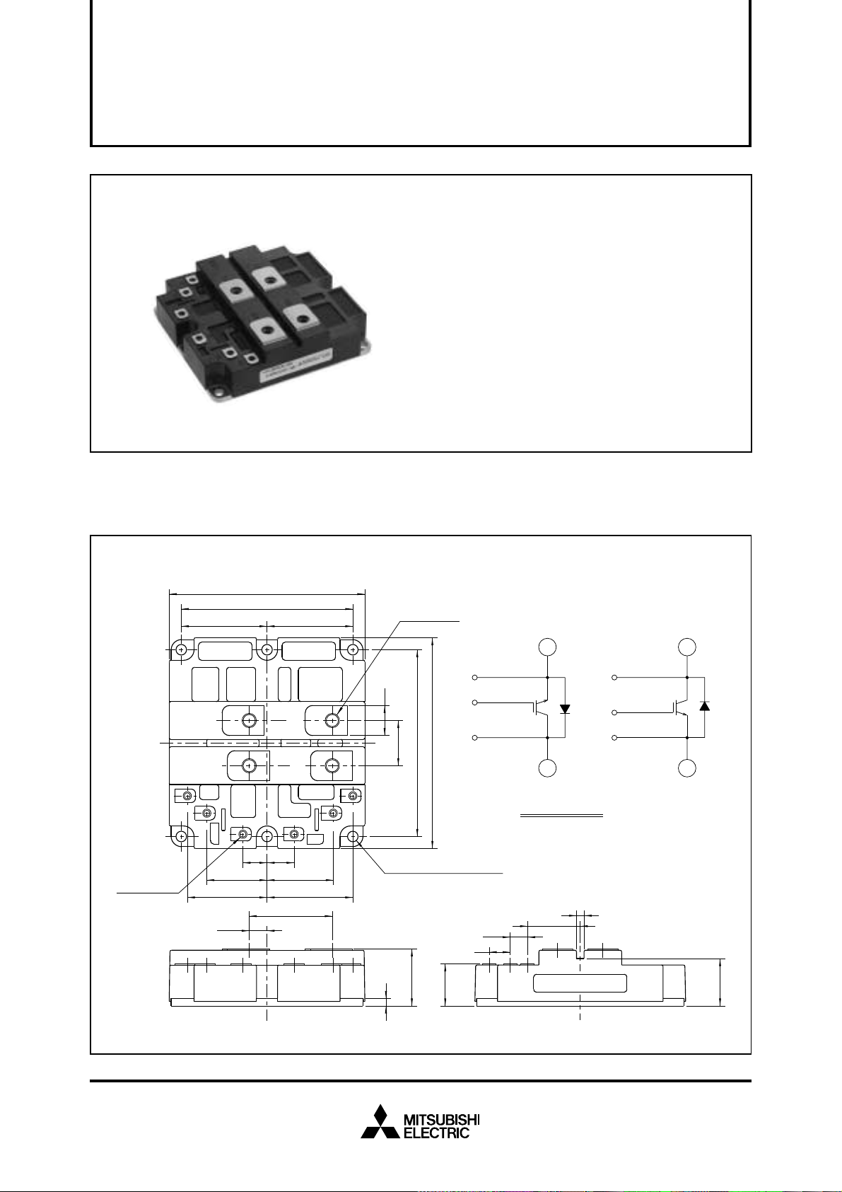
MITSUBISHI HVIGBT MODULES
CM800DZ-34H
3rd-Version HVIGBT (High Voltage Insulated Gate Bipolar Transistor) Modules
INSULATED TYPE
CM800DZ-34H
● IC...................................................................800A
HIGH POWER SWITCHING USE
● V
CES ....................................................... 1700V
● Insulated T ype
● 2-elements in a pack
APPLICATION
Inverters, Converters, DC choppers, Induction heating, DC to DC converters.
OUTLINE DRAWING & CIRCUIT DIAGRAM Dimensions in mm
130
6 - M4 NUTS
114
57±0.25 57±0.25
E1
C1
CM
E1 E2
C1
G1 G2
11.85
C2
E2
C2
16
18
4440
5753
55.2
4 - M8 NUTS
E1
20
±0.25
30
124
6 - φ 7 MOUNTING HOLES
140
G1
C1
14
11.5
E1
C1
CIRCUIT DIAGRAM
5
35
C2
C2
G2
E2
E2
38
5
HVIGBT MODULES (High Voltage Insulated Gate Bipolar Transistor Modules)
28
LABEL
31.5
Oct. 2002
Page 3
MITSUBISHI HVIGBT MODULES
CM800DZ-34H
HIGH POWER SWITCHING USE
3rd-Version HVIGBT (High Voltage Insulated Gate Bipolar Transistor) Modules
MAXIMUM RATINGS (Tj = 25°C)
Symbol Item Conditions UnitRatings
VCES
VGES
IC
ICM
IE
IEM
PC
Tj
Tstg
Viso
Collector-emitter voltage
Gate-emitter voltage
Collector current
(Note 2)
Emitter current
(Note 2)
Maximum collector dissipation
(Note 3)
Junction temperature
Storage temperature
Isolation voltage
—
Mounting torque
—
Mass
VGE = 0V
CE = 0V
V
T
C = 25°C
Pulse (Note 1)
T
C = 25°C
Pulse (Note 1)
C = 25°C, IGBT part
T
—
—
Charged part to base plate, rms, sinusoidal, AC 60Hz 1min.
Main terminals screw M8
Mounting screw M6
Auxiliary terminals screw M4
Typical value
–40 ~ +150
–40 ~ +125
6.67 ~ 13.00
2.84 ~ 6.00
0.88 ~ 2.00
INSULATED TYPE
1700
±20
800
1600
800
1600
5000
4000
N·m
N·m
N·m
1.0
V
V
A
A
A
A
W
°C
°C
V
kg
ELECTRICAL CHARACTERISTICS (Tj = 25°C)
Symbol
I
CES
V
GE(th)
IGES
VCE(sat)
Cies
Coes
Cres
QG
td (on)
tr
td (off)
tf
VEC
trr
Qrr
Rth(j-c)Q
Rth(j-c)R
Rth(c-f)
Note 1. Pulse width and repetition rate should be such that the device junction temp. (Tj) does not exceed Tjmax rating.
Collector cutoff current
Gate-emitter
threshold voltage
Gate-leakage current
Collector-emitter
saturation voltage
Input capacitance
Output capacitance
Reverse transfer capacitance
Total gate charge
Turn-on delay time
Turn-on rise time
Turn-off delay time
Turn-off fall time
(Note 2)
Emitter-collector voltage
(Note 2)
Reverse recovery time
(Note 2)
Reverse recovery charge
Thermal resistance
Contact thermal resistance
2. I
E, VEC, trr, Qrr & die/dt represent characteristics of the anti-parallel, emitter to collector free-wheel diode.
3. Junction temperature (T
4. Pulse width and repetition rate should be such as to cause negligible temperature rise.
Item Conditions
V
CE = VCES, VGE = 0V
IC = 80mA, VCE = 10V
V
GE = VGES, VCE = 0V
T
j = 25°C
j = 125°C
T
CE = 10V
V
V
GE = 0V
CC = 850V, IC = 800A, VGE = 15V
V
V
CC = 850V, IC = 800A
V
GE1 = VGE2 = 15V
R
G = 3.3Ω
I
C = 800A, VGE = 15V (Note 4)
Resistive load switching operation
I
E = 800A, VGE = 0V
I
E = 800A
die / dt = –1600A / µs
Junction to case, IGBT part (Per 1/2 module)
Junction to case, FWDi part (Per 1/2 module)
Case to fin, conductive grease applied (Per 1/2 module)
j) should not increase beyond 150°C.
Min Typ Max
Limits
—
—
5.54.5 6.5
—
—
—
—
—
—
—
—
—
—
—
—
—
—
—
—
—
—
2.80
3.20
72
9.0
3.6
6.6
—
—
—
—
2.60
—
150
—
—
0.020
0.025
0.043
12
0.5
3.64
—
—
—
—
—
1.60
2.00
2.70
0.80
3.38
2.70
—
—
Unit
mA
V
µA
V
nF
nF
nF
µC
µs
µs
µs
µs
V
µs
µC
K/W
K/W
K/W
HVIGBT MODULES (High Voltage Insulated Gate Bipolar Transistor Modules)
Oct. 2002
Page 4

SECURITY
CODE
SPEC.NAME
Application
Note
Prepared by S.Iura S.Iura
Checked by M.Yamamoto I.Umesaki
Approved by M.Yamamoto M.Tabata
DATE Apr.8.2002
MITSUBISHI ELECTRIC CORPORATION
A
R
E
V
Aug.2.2002
Data Sheet
(CM800DZ−34H)
1. Output characteristics Page 2
2. Transfer characteristics Page 3
3. Collector-emitter saturation voltage characteristics Page 4 / 5
4. Free wheel diode forward characteristics Page 6
5. Capacitance characteristics Page 7
6. Gate charge characteristics Page 8
7. Half-bridge Switching time characteristics Page 9
8. Half-bridge Switching energy characteristics Page 10
9. Reverse recovery characteristics Page 11
10. Transient thermal impedance characteristics Page 12
A
11. Turn-off switching safe operating area Page 13
12. Short circuit safe operating area Page 14
13. Reverse recovery safe operating area Page 15
HVIGBT
HVM-1005-A
(P2-OU)
PAGE
1 / 15
Page 5
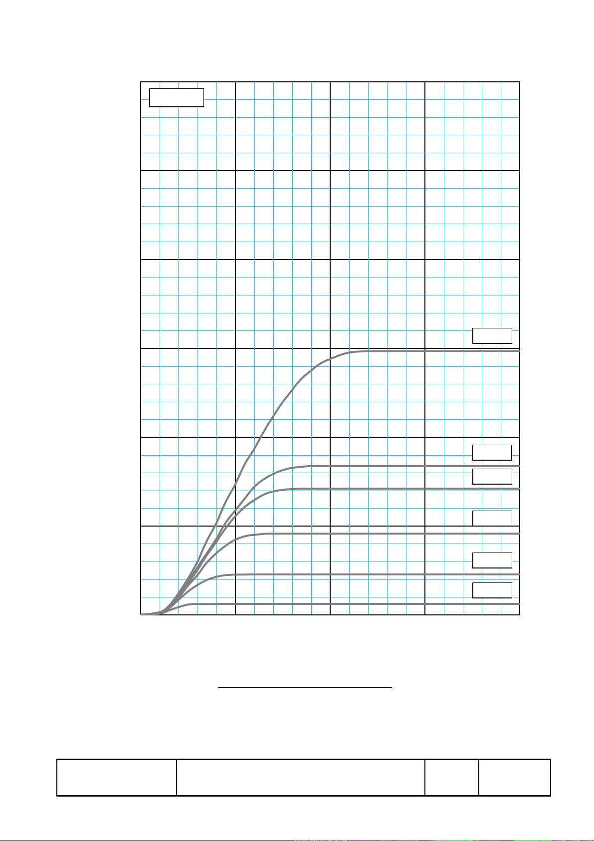
12000
Tj=25°C
10000
8000
6000
COLLECTOR CURRENT [A]
4000
2000
0
0 5 10 15 20
VGE=20V
VGE=15V
VGE=14V
VGE=12V
VGE=10V
VGE= 8V
HVIGBT
COLLECTOR-EMITTER VOLTAGE [V]
Output characteristics (typical)
HVM-1005-A
PAGE
(P2-OU)
2 / 15
Page 6
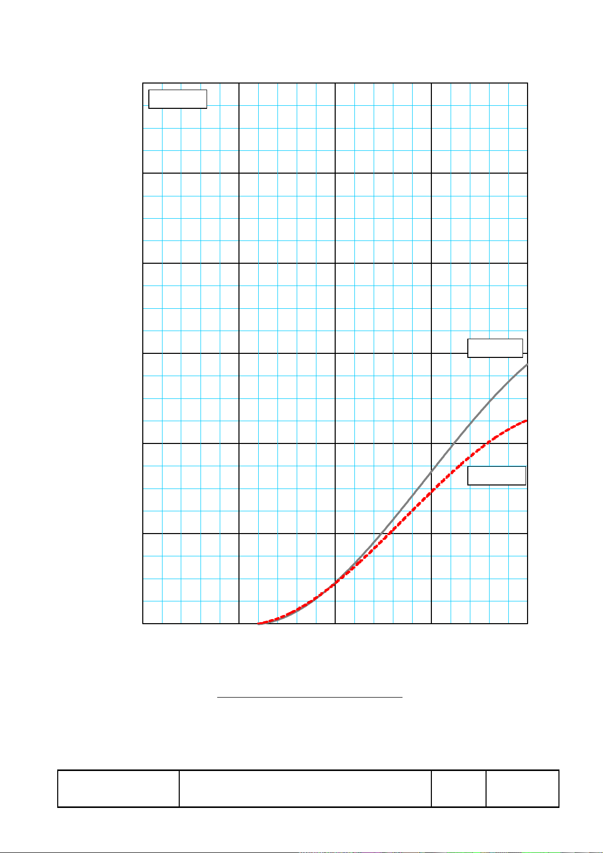
12000
VCE=10V
10000
8000
6000
COLLECTOR CURRENT [A]
4000
2000
0
0 5 10 15 20
Tj=25°C
Tj=125°C
HVIGBT
GATE-EMITTER VOLTAGE [V]
Transfer characteristics (typical)
HVM-1005-A
PAGE
(P2-OU)
3 / 15
Page 7

6
VGE=15V
5
Tj=125°C
4
Tj=25°C
3
2
COLLECTOR-EMITTER VOLTAGE [V]
1
0
0 500 1000 1500 2000
HVIGBT
COLLECTOR CURRENT [A]
Collector-emitter saturation voltage characteristics (typical)
HVM-1005-A
(P2-OU)
PAGE
4 / 15
Page 8

10
Tj=25°C
9
8
7
6
5
4
3
COLLECTOR-EMITTER SATURATION VOLTAGE [V]
2
1
0
0 5 10 15 20
Ic = 1600A
Ic = 800A
Ic = 400A
HVIGBT
GATE-EMITTER VOLTAGE [V]
Collector-emitter saturation voltage characteristics (typical)
HVM-1005-A
(P2-OU)
PAGE
5 / 15
Page 9

5
4
Tj=25°C
3
Tj=125°C
2
EMITTER-COLLECTOR VOLTAGE [V]
1
0
0 500 1000 1500 2000
HVIGBT
EMITTER CURRENT [A]
Free wheel diode forward voltage characteristics (typical)
HVM-1005-A
(P2-OU)
PAGE
6 / 15
Page 10

1000
VGE=15V, Tj=25°C
: f=100kHz
C
ies
: f=100kHz
C
oes
: f=1MHz
C
res
100
CAPACITANCE [nF]
10
C
ies
C
oes
C
res
HVIGBT
1
0.1 1 10 100
COLLECTOR-EMITTER VOLTAGE [V]
Capacitance characteristics (typical)
PAGE
HVM-1005-A
(P2-OU)
7 / 15
Page 11

20
VCC=850V
=800A
I
C
18
16
14
12
10
8
GATE-EMITTER VOLTAGE [V]
6
4
2
0
0 2500 5000 7500 10000
HVIGBT
GATE CHARGE [nC]
Gate charge characteristics (typical)
HVM-1005-A
(P2-OU)
PAGE
8 / 15
Page 12

10
VCC=850V, VGE=±15V
=3.3Ω, Tj=125°C, LS=150nH
R
G
Inductive load
t
t
tr
d(off)
d(on)
1
s]
µ
SWITCHING TIME [
0.1
0.01
10 100 1000 10000
tf
COLLECTOR CURRENT [A]
HVIGBT
Half-bridge switching time characteristics (typical)
HVM-1005-A
(P2-OU)
PAGE
9 / 15
Page 13

1.2
VCC=850V, VGE=±15V
=3.3Ω, Tj=125°C, LS=150nH
R
G
Inductive load
Integrated over range of 10%
1
0.8
0.6
SWITCHING ENERGY [J/P]
0.4
0.2
Eon
E
off
E
rec
0
HVIGBT
0 400 800 1200 1600
COLLECTOR / EMITTER CURRENT [A]
Half-bridge switching energy characteristics (typical)
HVM-1005-A
(P2-OU)
PAGE
10 / 15
Page 14

s]
µ
100
10
VCC=850V, Tj=125°C
=150nH, Inductive load
L
S
IGBT drive conditions
=±15V, RG=3.3Ω
V
GE
10000
1000
Irr
trr
REVERSE RECOVERY TIME [
1
0.1
10 100 1000 10000
EMITTER CURRENT [A]
Reverse recovery characteristics (typical)
100
10
REVERSE RECOVERY CURRENT [A]
HVIGBT
HVM-1005-A
(P2-OU)
PAGE
11 / 15
Page 15

j
=0.034 K/W
=0.020 K/W
-c)
th(
th(j-c)
: R
.
Single pulse
Tc = 25°C
IGBT part
FWDi part: R
TIME [second]
0.001 0.010 0.100 1.000 10.000
1.2
1.0
0.8
0.6
0.4
0.2
0.0
NORMALIZED TRANSIENT THERMAL IMPEDANCE
Transient thermal impedance characteristics
HVIGBT
HVM-1005-A
(P2-OU)
PAGE
12 / 15
Page 16

3000
VCC≤1150V, VGE=±15V
≥3.3Ω, Tj=125°C
R
G
2500
2000
1500
COLLECTOR CURRENT [A]
1000
500
0
0 500 1000 1500 2000
HVIGBT
COLLECTOR-EMITTER VOLTAGE [V]
Turn-off switching safe operating area (SWSOA / RBSOA)
HVM-1005-A
(P2-OU)
PAGE
13 / 15
Page 17

6000
VCC≤1150V, VGE=±15V
≥3.3Ω, Tj=125°C
R
G
tw≤10µs
5000
4000
3000
COLLECTOR CURRENT [A]
2000
1000
0
0 500 1000 1500 2000
HVIGBT
COLLECTOR-EMITTER VOLTAGE [V]
Short circuit safe operating area (SCSOA)
HVM-1005-A
(P2-OU)
PAGE
14 / 15
Page 18

2500
VCC≤1150V, Tj=125°C
di/dt≤1800A/µs
2000
1500
1000
REVERSE RECOVERY CURRENT [A]
500
0
0 500 1000 1500 2000
EMITTER-COLLECTOR VOLTAGE [V]
Reverse recovery safe operating area (RRSOA / Di-SOA)
HVIGBT
HVM-1005-A
(P2-OU)
PAGE
15 / 15
 Loading...