

Page 1

6121 Baker Road,
Suite 108
Minnetonka, MN 55345
www.chtechnology.com
Phone (952) 933-6190
Fax (952) 933-6223
1-800-274-4284
Thank you for downloading this document from C&H Technology, Inc.
Please contact the C&H Technology team for the following questions -
Technical
Application
Assembly
Availability
Pricing
Phone – 1-800-274-4284
E-Mail – sales@chtechnology.com
www.chtechnology.com - SPECIALISTS IN POWER ELECTRONIC COMPONENTS AND ASSEMBLIES - www.chtechnology.com
Page 2
CM75TX-24S
Powerex, Inc., 173 Pavilion Lane, Youngwood, Pennsylvania 15697 (724) 925-7272
www.pwrx.com
AE
DETAIL "A"
AJ
AH
AG
DETAIL "B"
2
A
E
F
G
K
KQ
JMMM
52 51 50 49 48 47 46 45 44 43 42 41 40 39 38 37 36 35 34 33 32 31
53
54
N
K
55
(4 PLACES)
K
56
57
L
58
59
K
60
K
61
V
12345678910111213141516171819202122
W
U
X
P(54~56)
N(59~61)
Caution: Each (three) pin terminal of P/N/P1/N1/U/V/W is connected in the module,
however, all three pins should be used for external wiring.
LHLLLL
UP(1)
G
E
UP(2)
U(48~50) V(42~44) W(36~38)
G
UN(5)
K
K
D
DETAIL "A"
K
DETAIL "B"
VP(9)
G
E
VP(10)
G
VN(13)
K
K
30
K
29
K
28
27
R B
L
26
25
K
24
K
23
KKKKKK
Tolerance Otherwise Specified (mm)
Y
WP(17)
G
E
WP(18)
WN(21)
G
EWN(22)EVN(14)EUN(6)
AD
K
AC
AA
AB
C
Z
S
P
AH
T
Division of Dimension Tolerance
0.5 to 3 ±0.2
over 3 to 6 ±0.3
over 6 to 30 ±0.5
over 30 to 120 ±0.8
over 120 to 400 ±1.2
The tolerance of size between
terminals is assumed to ±0.4
P1(28~30)
TH
TH1
(31)
(32)
N1(23~25)
Outline Drawing and Circuit Diagram
Dimensions Inches Millimeters
A 4.79 121.7
B 2.44 62.0
C 0.51 13.0
D 4.49 114.05
E 4.33±0.02 110.0±0.5
F 3.9 99.0
G 3.72 94.5
H 0.59 15.0
J 0.96 24.52
K 0.15 3.81
L 0.45 11.43
M 0.6 15.24
N 0.22 Dia. 5.5 Dia.
P 2.13 54.2
Q 0.30 7.75
R 1.97±0.02 50.0±0.5
S 2.26 57.5
Dimensions Inches Millimeters
U 0.16 4.06
V 0.46 11.66
W 0.14 3.75
X 0.14 3.5
Y 0.03 0.8
Z 0.28 7.0
AA 0.81 20.5
AB 0.67 17.0
AC 0.03 0.65
AD 0.05 1.15
AE 0.29 7.4
AF 0.047 1.2
AG 0.49 12.5
AH 0.12 3.0
AJ 0.17 Dia. 4.3 Dia.
AK 0.102 Dia. 2.6 Dia.
AL 0.088 Dia. 2.25 Dia.
T 0.165 4.2
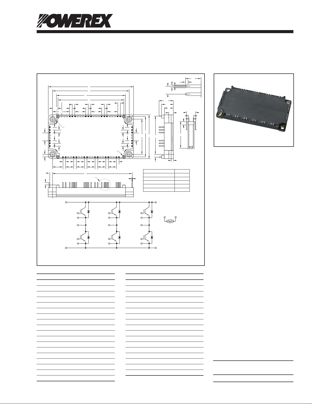
Six IGBTMOD™
NX-S Series Module
75 Amperes/1200 Volts
AF
AK
AL
Description:
Powerex IGBTMOD™ Modules
are designed for use in switching
applications. Each module
consists of six IGBT Transistors in
a three phase bridge configuration
with each transistor having a
reverse-connected super-fast
recovery free-wheel diode. All
components and interconnects
are isolated from the heat sinking
baseplate, offering simplified
system assembly and thermal
management.
Features:
£ Low Drive Power
£ Low V
£ Discrete Super-Fast Recovery
£ Isolated Baseplate for Easy
Applications:
£ AC Motor Control
£ Motion/Servo Control
£ Photovoltaic/Fuel Cell
Ordering Information:
Example: Select the complete
module number you desire from
the table below -i.e.
CM75TX-24S is a 1200V (V
75 Ampere Six IGBTMOD™ Power
Module.
Type Current Rating
Amperes Volts (x 50)
CM 75 24
CE(sat)
Free-Wheel Diode
Heat Sinking
V
CES
CES
),
106/11 Rev. 2
Page 3
Powerex, Inc., 173 Pavilion Lane, Youngwood, Pennsylvania 15697 (724) 925-7272 www.pwrx.com
CM75TX-24S
Six IGBTMOD™ NX-S Series Module
75 Amperes/1200 Volts
Absolute Maximum Ratings, Tj = 25°C unless otherwise specied
Inverter Part IGBT/FWDi
Characteristics Symbol Rating Units
Collector-Emitter Voltage (VGE = 0V) V
Gate-Emitter Voltage (VCE = 0V) V
Collector Current (DC, TC = 122°C)
*2,*3
IC 75 Amperes
Collector Current (Pulse)*4 I
Total Power Dissipation (TC = 25°C)
Emitter Current (TC = 25°C)
*2,*3
P
*2,*3
I
Emitter Current (Pulse)*4 I
1200 Volts
CES
±20 Volts
GES
150 Amperes
CRM
600 Watts
tot
*1
75 Amperes
E
*1
150 Amperes
ERM
Module
Characteristics Symbol Rating Units
Maximum Junction Temperature T
Maximum Case Temperature*2 T
Operating Junction Temperature T
Storage Temperature T
Isolation Voltage (Terminals to Baseplate, f = 60Hz, AC 1 minute) V
*1 Represent ratings and characteristics of the anti-parallel, emitter-to-collector free wheeling
diode (FWDi).
*2 Case temperature (TC) and heatsink temperature (Ts) is measured on the surface
(mounting side) of the baseplate and the heatsink side just under the chips.
Refer to the figure to the right for chip location.
The heatsink thermal resistance should be measured just under the chips.
*3 Junction temperature (Tj) should not increase beyond maximum junction
temperature (T
*4 Pulse width and repetition rate should be such that device junction temperature (Tj)
does not exceed T
j(max)
) rating.
j(max)
rating.
0 0
19.9
28.4
Each mark points to the center position of each chip.
Tr*P / Tr*N: IGBT Di*P / Di*N: FWDi Th: NTC Thermistor
175 °C
j(max)
125 °C
C(max)
-40 to +150 °C
j(op)
-40 to +125 °C
stg
2500 Volts
ISO
20.6033.1
52 51 50 49 48 47 46 45 44 4342 41 40 39 38 37 36 35 34 33 32 31
53
Di
54
UP
55
56
Tr
57
UP
58
59
60
61
1 2 3 4 5 6 7 8 9 10 11 12 13 14 15 16 17 18 19 20 21 22
51.6
64.1
82.6
96.1
104.5
Di
Di
VP
UN
Tr
Tr
VP
UN
Di
Di
WP
VN
Tr
Tr
WP
VN
30
Di
29
WN
Th
28
27
Tr
26
WN
25
24
23
LABEL SIDE
21.6
24.1
30.0
2 06/11 Rev. 2
Page 4

Powerex, Inc., 173 Pavilion Lane, Youngwood, Pennsylvania 15697 (724) 925-7272 www.pwrx.com
CM75TX-24S
Six IGBTMOD™ NX-S Series Module
75 Amperes/1200 Volts
Electrical Characteristics, Tj = 25°C unless otherwise specied
Inverter Part IGBT/FWDi
Characteristics Symbol Test Conditions Min. Typ. Max. Units
Collector-Emitter Cutoff Current I
Gate-Emitter Leakage Current I
Gate-Emitter Threshold Voltage V
Collector-Emitter Saturation Voltage V
(Terminal) IC = 75A, VGE = 15V, Tj = 125°C*5 — 2.00 — Volts
IC = 75A, VGE = 15V, Tj = 150°C*5 — 2.05 — Volts
Collector-Emitter Saturation Voltage V
(Chip) IC = 75A, VGE = 15V, Tj = 125°C*5 — 1.90 — Volts
IC = 75A, VGE = 15V, Tj = 150°C*5 — 1.95 — Volts
Input Capacitance C
Output Capacitance C
Reverse Transfer Capacitance C
Gate Charge QG VCC = 600V, IC = 75A, VGE = 15V — 175 — nC
Turn-on Delay Time t
Rise Time tr VCC = 600V, IC = 75A, VGE = ±15V, — — 200 ns
Turn-off Delay Time t
Fall Time tf — — 300 ns
Emitter-Collector Voltage V
(Terminal) IE = 75A, VGE = 0V, Tj = 125°C*5 — 1.80 — Volts
IE = 75A, VGE = 0V, Tj = 150°C*5 — 1.80 — Volts
Emitter-Collector Voltage V
(Chip) IE = 75A, VGE = 0V, Tj = 125°C*5 — 1.70 — Volts
IE = 75A, VGE = 0V, Tj = 150°C*5 — 1.70 — Volts
Reverse Recovery Time t
Reverse Recovery Charge Q
Internal Lead Resistance R
Per Switch,TC = 25°C
Internal Gate Resistance rg Per Switch — 0 — Ω
*1 Represent ratings and characteristics of the anti-parallel, emitter-to-collector free wheeling
diode (FWDi).
*2 Case temperature (TC) and heatsink temperature (Ts) is measured on the surface
(mounting side) of the baseplate and the heatsink side just under the chips.
Refer to the figure to the right for chip location.
The heatsink thermal resistance should be measured just under the chips.
*5 Pulse width and repetition rate should be such as to cause negligible temperature rise.
VCE = V
CES
VGE = V
GES
IC = 7.5mA, VCE = 10V 5.4 6 6.6 Volts
GE(th)
IC = 75A, VGE = 15V, Tj = 25°C*5 — 1.80 2.25 Volts
CE(sat)
IC = 75A, VGE = 15V, Tj = 25°C*5 — 1.70 2.15 Volts
CE(sat)
— — 7.5 nF
ies
VCE = 10V, VGE = 0V — — 1.5 nF
oes
— — 0.13 nF
res
— — 300 ns
d(on)
RG = 8.2Ω, Inductive Load — — 600 ns
d(off)
*1
IE = 75A, VGE = 0V, Tj = 25°C*5 — 1.80 2.25 Volts
EC
*1
IE = 75A, VGE = 0V, Tj = 25°C*5 — 1.70 2.15 Volts
EC
*1
VCC = 600V, IE = 75A, VGE = ±15V — — 300 ns
rr
*1
RG = 8.2Ω, Inductive Load — 4.0 — µC
rr
CC' + EE'
Main Terminals-Chip, — — 2.4 mΩ
, VGE = 0V — — 1 mA
CES
, VCE = 0V — — 0.5 µA
GES
*2
0 0
19.9
28.4
20.6033.1
52 51 50 49 48 47 46 45 44 4342 41 40 39 38 37 36 35 34 33 32 31
53
Di
54
UP
55
56
Tr
57
UP
58
59
60
61
1 2 3 4 5 6 7 8 9 10 11 12 13 14 15 16 17 18 19 20 21 22
Each mark points to the center position of each chip.
Tr*P / Tr*N: IGBT Di*P / Di*N: FWDi Th: NTC Thermistor
51.6
64.1
82.6
96.1
104.5
Di
Di
VP
UN
Tr
Tr
VP
UN
Di
Di
WP
VN
Tr
Tr
WP
VN
30
Di
29
WN
Th
28
27
Tr
26
WN
25
24
23
LABEL SIDE
21.6
24.1
30.0
306/11 Rev. 2
Page 5

Powerex, Inc., 173 Pavilion Lane, Youngwood, Pennsylvania 15697 (724) 925-7272 www.pwrx.com
CM75TX-24S
Six IGBTMOD™ NX-S Series Module
75 Amperes/1200 Volts
Electrical Characteristics, Tj = 25°C unless otherwise specied (continued)
NTC Thermistor Part
Characteristics Symbol Test Conditions Min. Typ. Max. Units
Zero Power Resistance R25 TC = 25°C*2 4.85 5.00 5.15 kΩ
Deviation of Resistance ∆R/R TC = 100°C, R
B Constant B
Approximate by Equation*6 — 3375 — K
(25/50)
= 493Ω -7.3 — +7.8 %
100
Power Dissipation P25 TC = 25°C*2 — — 10 mW
Thermal Resistance Characteristics
Thermal Resistance, Junction to Case*2 R
Thermal Resistance, Junction to Case*2 R
Contact Thermal Resistance, R
Case to Heatsink*2 Per 1 Module
Q IGBT Part, Per 1/6 Module — — 0.25 K/W
th(j-c)
D FWDi Part, Per 1/6 Module — — 0.40 K/W
th(j-c)
Thermal Grease Applied, — 0.015 — K/W
th(c-f)
*7
Mechanical Characteristics
Mounting Torque Ms Mounting to Heatsink, M5 Screw 22 27 31 in-lb
Weight m — 300 — Grams
Creepage Distance ds Terminal to Terminal 10.28 — — mm
Terminal to Baseplate 14.27 — — mm
Clearance da Terminal to Terminal 10.28 — — mm
Terminal to Baseplate 12.33 — — mm
Flatness of Baseplate ec On Centerline X, Y*8 ±0 — ±100 µm
Recommended Operating Conditons, Ta = 25°C
DC Supply Voltage VCC Applied Across P-N/P1-N1 Terminals — 600 850 Volts
Gate-Emitter Drive Voltage V
G*P-Es*P/G*N-Es*N Terminals
External Gate Resistance RG Per Switch 8.2 — 82 Ω
*2 Case temperature (TC) and heatsink temperature (Ts) is measured on the surface
(mounting side) of the baseplate and the heatsink side just under the chips.
Refer to the figure to the right for chip location.
The heatsink thermal resistance should be measured just under the chips.
*6 B
(25/50)
R
R25; Resistance at Absolute Temperature T25 [K]; T25 = 25 [°C] + 273.15 = 298.15 [K]
R50; Resistance at Absolute Temperature T50 [K]; T50 = 50 [°C] + 273.15 = 323.15 [K]
*7 Typical value is measured by using thermally conductive grease of λ = 0.9 [W/(m • K)].
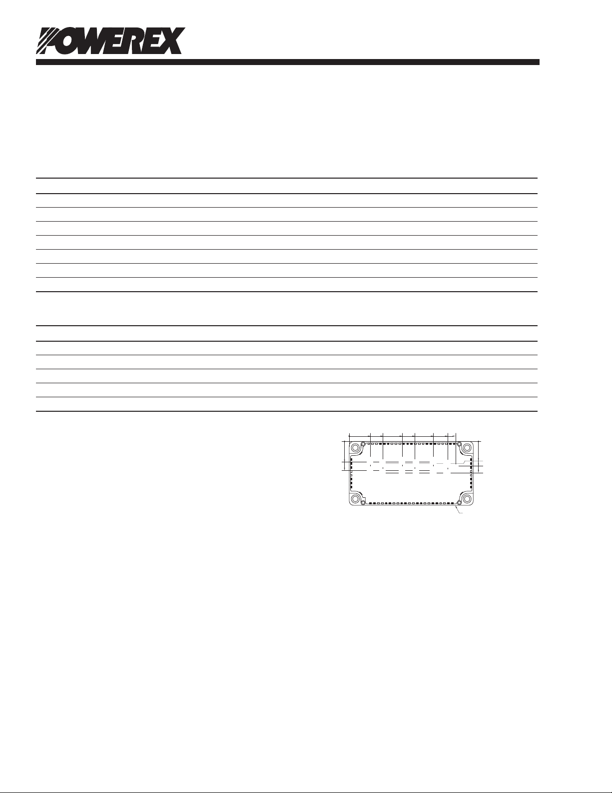
*8 Baseplate (mounting side) flatness measurement points (X, Y) are shown in the figure below.
= In(
R
25
)/( 1 –
50 T25 T50
MOUNTING SIDE
1
)
MOUNTING SIDE
+ : CONVEX
– : CONCAVE
X
Applied Across 13.5 15.0 16.5 Volts
GE(on)
Y
MOUNTING
SIDE
0 0
19.9
28.4
20.6033.1
52 51 50 49 48 47 46 45 44 4342 41 40 39 38 37 36 35 34 33 32 31
53
Di
54
UP
55
56
Tr
57
UP
58
59
60
61
1 2 3 4 5 6 7 8 9 10 11 12 13 14 15 16 17 18 19 20 21 22
Each mark points to the center position of each chip.
Tr*P / Tr*N: IGBT Di*P / Di*N: FWDi Th: NTC Thermistor
51.6
64.1
82.6
Di
Di
VP
UN
Tr
Tr
VP
UN
Di
Di
VN
Tr
VN
Di
WP
WN
Tr
Tr
WP
WN
– : CONCAVE
+ : CONVEX
96.1
104.5
Th
30
29
28
27
26
25
24
23
LABEL SIDE
21.6
24.1
30.0
4 06/11 Rev. 2
Page 6
Powerex, Inc., 173 Pavilion Lane, Youngwood, Pennsylvania 15697 (724) 925-7272 www.pwrx.com
CM75TX-24S
Six IGBTMOD™ NX-S Series Module
75 Amperes/1200 Volts
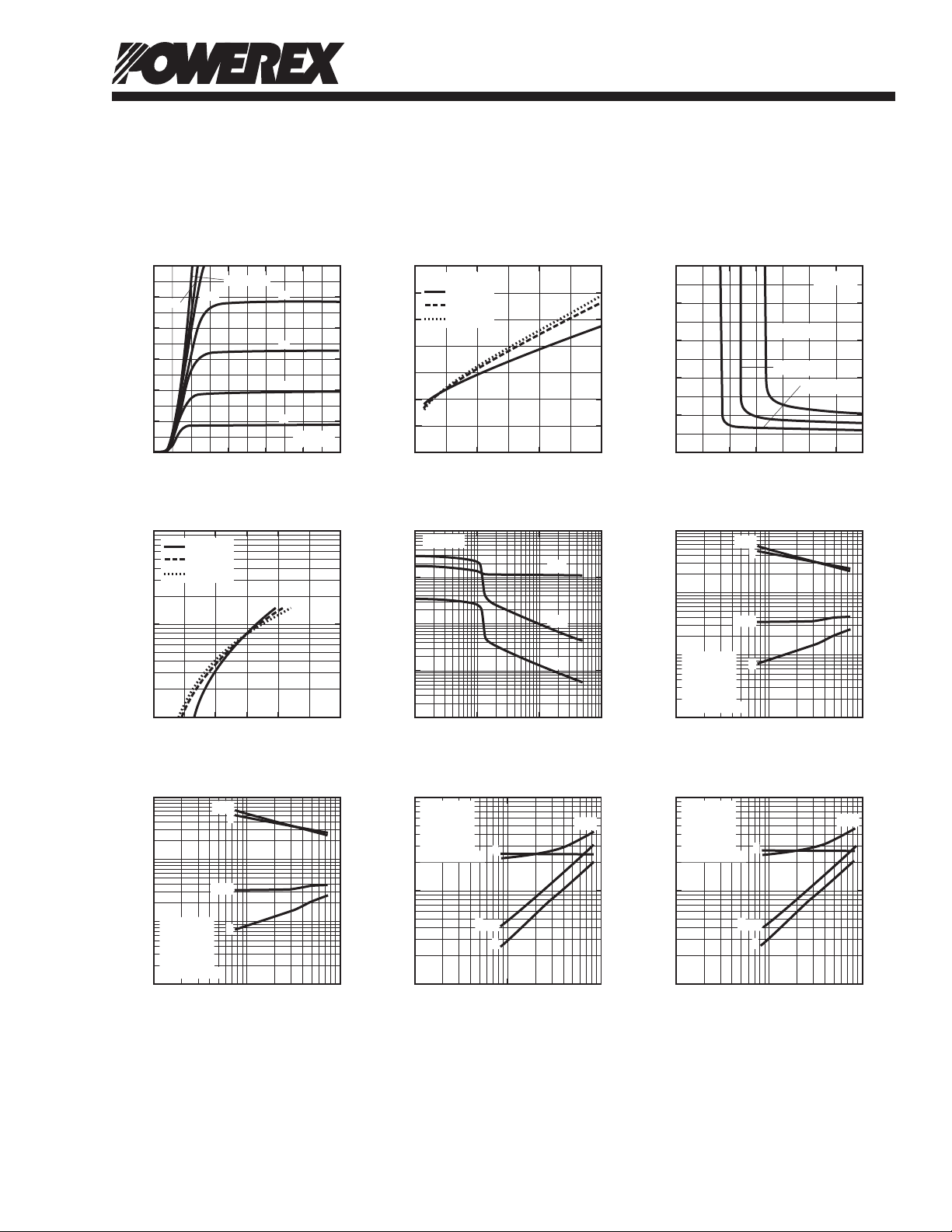
OUTPUT CHARACTERISTICS
(TYPICAL)
150
VGE = 20V
125
13.5
15
100
, (AMPERES)
C
75
50
25
COLLECTOR CURRENT, I
0
0 2 4 6 8 10
COLLECTOR-EMITTER VOLTAGE, VCE, (VOLTS)
FREE-WHEEL DIODE
FORWARD CHARACTERISTICS
3
10
, (AMPERES)
E
2
10
EMITTER CURRENT, I
1
10
0 1.0 0.5 2.51.5 2.0 3.0
EMITTER-COLLECTOR VOLTAGE, V
SWITCHING CHARACTERISTICS
3
10
2
10
Tj = 25°C
= 125°C
T
j
= 150°C
T
j
t
t
d(on)
(TYPICAL)
HALF-BRIDGE
(TYPICAL)
d(off)
t
f
12
11
10
9
Tj = 25°C
, (VOLTS)
EC
SATURATION VOLTAGE CHARACTERISTICS
3.5
3.0
, (VOLTS)
2.5
CE(sat)
2.0
COLLECTOR-EMITTER
VGE = 15V
Tj = 25°C
= 125°C
T
j
= 150°C
T
j
(TYPICAL)
1.5
COLLECTOR-EMITTER
1.0
0.5
SATURATION VOLTAGE, V
0
0
COLLECTOR CURRENT, IC, (AMPERES)
CAPACITANCE VS. V
2
10
VGE = 0V
, (nF)
1
10
res
, C
oes
, C
ies
0
10
-1
10
CAPACITANCE, C
-2
10
-1
10
COLLECTOR-EMITTER VOLTAGE, VCE, (VOLTS)
3
10
VCC = 600V
V
GE
I
= 75A
C
T
= 125°C
j
Inductive Load
2
10
(TYPICAL)
0
10
SWITCHING TIME VS.
GATE RESISTANCE
(TYPICAL)
= ±15V
t
f
SATURATION VOLTAGE CHARACTERISTICS
10
8
, (VOLTS)
CE(sat)
6
4
COLLECTOR-EMITTER
COLLECTOR-EMITTER
(TYPICAL)
Tj = 25°C
IC = 150A
IC = 75A
IC = 30A
2
SATURATION VOLTAGE, V
0
15010050
CE
C
ies
C
oes
C
res
t
d(off)
2
10
1
10
6 8 10 1412 16 18 20
GATE-EMITTER VOLTAGE, VGE, (VOLTS)
HALF-BRIDGE
SWITCHING CHARACTERISTICS
3
10
2
10
1
10
VCC = 600V
SWITCHING TIME, (ns)
V
GE
R
= 8.2Ω
G
T
= 125°C
j
Inductive Load
0
10
0
10
COLLECTOR CURRENT, IC, (AMPERES)
3
10
VCC = 600V
V
GE
I
= 75A
C
T
= 150°C
j
Inductive Load
2
10
(TYPICAL)
t
d(off)
t
f
t
d(on)
t
= ±15V
r
10
SWITCHING TIME VS.
GATE RESISTANCE
(TYPICAL)
= ±15V
t
f
1
t
d(off)
2
10
1
10
VCC = 600V
SWITCHING TIME, (ns)
V
= ±15V
GE
R
= 8.2Ω
G
T
= 150°C
j
Inductive Load
0
10
0
10
COLLECTOR CURRENT, I
t
t
r
1
10
, (AMPERES)
C
10
2
SWITCHING TIME, (ns)
1
10
0
10
d(on)
t
r
1
EXTERNAL GATE RESISTANCE, R
10
SWITCHING TIME, (ns)
1
2
10
, (Ω)
G
10
0
10
t
d(on)
t
r
1
EXTERNAL GATE RESISTANCE, R
10
2
10
, (Ω)
G
506/11 Rev. 2
Page 7

Powerex, Inc., 173 Pavilion Lane, Youngwood, Pennsylvania 15697 (724) 925-7272 www.pwrx.com
CM75TX-24S
Six IGBTMOD™ NX-S Series Module
75 Amperes/1200 Volts
REVERSE RECOVERY CHARACTERISTICS
3
10
VCC = 600V
V
GE
R
= 8.2Ω
2
10
1
10
10
G
T
= 125°C
j
Inductive Load
0
(ns)
rr
(A), t
rr
REVERSE RECOVERY, I
CHARACTERISTICS (TYPICAL)
1
10
V
CC
V
GE
R
, (mJ)
rr
, (mJ)
off
, E
on
SWITCHING ENERGY, E
REVERSE RECIVERY ENERGY, E
10
= 8.2Ω
G
T
= 125°C
j
0
10
-1
0
10
COLLECTOR CURRENT, IC, (AMPERES)
CHARACTERISTICS (TYPICAL)
2
10
V
CC
V
GE
I
= 75A
C
, (mJ)
rr
, (mJ)
T
= 150°C
off
, E
on
SWITCHING ENERGY, E
j
1
10
REVERSE RECIVERY ENERGY, E
0
10
0
10
(TYPICAL)
= ±15V
I
rr
t
rr
1
EMITTER CURRENT, IE, (AMPERES)
10
HALF-BRIDGE SWITCHING
= 600V
= ±15V
E
on
E
off
E
rr
1
10
EMITTER CURRENT, I
HALF-BRIDGE SWITCHING
= 600V
= ±15V
E
on
E
off
E
rr
1
10
GATE RESISTANCE, RG, (Ω)
, (AMPERES)
E
2
10
2
10
2
10
REVERSE RECOVERY CHARACTERISTICS
3
10
VCC = 600V
V
= ±15V
GE
R
= 8.2Ω
rr
rr
2
10
1
10
10
G
T
= 150°C
j
Inductive Load
0
(ns)
(A), t
REVERSE RECOVERY, I
CHARACTERISTICS (TYPICAL)
1
10
VCC = 600V
V
GE
R
, (mJ)
rr
, (mJ)
off
, E
on
SWITCHING ENERGY, E
REVERSE RECIVERY ENERGY, E
10
= 8.2Ω
G
T
= 150°C
j
0
10
-1
0
10
COLLECTOR CURRENT, IC, (AMPERES)
IMPEDANCE CHARACTERISTICS
10-310
0
th(j-c')
10
-1
10
Single Pulse
T
= 25°C
C
Per Unit Base =
R
th(j-c)
• (NORMALIZED VALUE)
-2
0.25°C/W
10
th
(IGBT)
= R
th
R
Z
th(j-c)
0.40°C/W
(FWDi)
-3
10
NORMALIZED TRANSIENT THERMAL IMPEDANCE, Z
(TYPICAL)
I
rr
t
rr
1
EMITTER CURRENT, IE, (AMPERES)
10
HALF-BRIDGE SWITCHING
= ±15V
E
on
E
off
E
rr
1
10
EMITTER CURRENT, I
, (AMPERES)
E
TRANSIENT THERMAL
(MAXIMUM)
-2
-1
10
10
=
=
-5
10
TIME, (s)
10
20
15
, (VOLTS)
GE
GATE CHARGE VS. V
VCC = 600V
I
= 75A
C
T
= 25°C
j
GE
10
5
GATE-EMITTER VOLTAGE, V
2
10
2
10
0
1
10
10
10
-4
10
-3
10
0
0
CHARACTERISTICS (TYPICAL)
2
10
V
= 600V
CC
V
= ±15V
GE
I
= 75A
C
, (mJ)
rr
, (mJ)
T
= 125°C
off
, E
on
SWITCHING ENERGY, E
-1
-2
-3
j
1
10
REVERSE RECIVERY ENERGY, E
0
10
0
10
50 100 150 200 250
GATE CHARGE, QG, (nC)
HALF-BRIDGE SWITCHING
E
on
E
off
E
rr
1
10
GATE RESISTANCE, RG, (Ω)
10
2
6 06/11 Rev. 2
 Loading...