

Page 1

6121 Baker Road,
Suite 108
Minnetonka, MN 55345
www.chtechnology.com
Phone (952) 933-6190
Fax (952) 933-6223
1-800-274-4284
Thank you for downloading this document from C&H Technology, Inc.
Please contact the C&H Technology team for the following questions -
Technical
Application
Assembly
Availability
Pricing
Phone – 1-800-274-4284
E-Mail – sales@chtechnology.com
www.chtechnology.com - SPECIALISTS IN POWER ELECTRONIC COMPONENTS AND ASSEMBLIES - www.chtechnology.com
Page 2
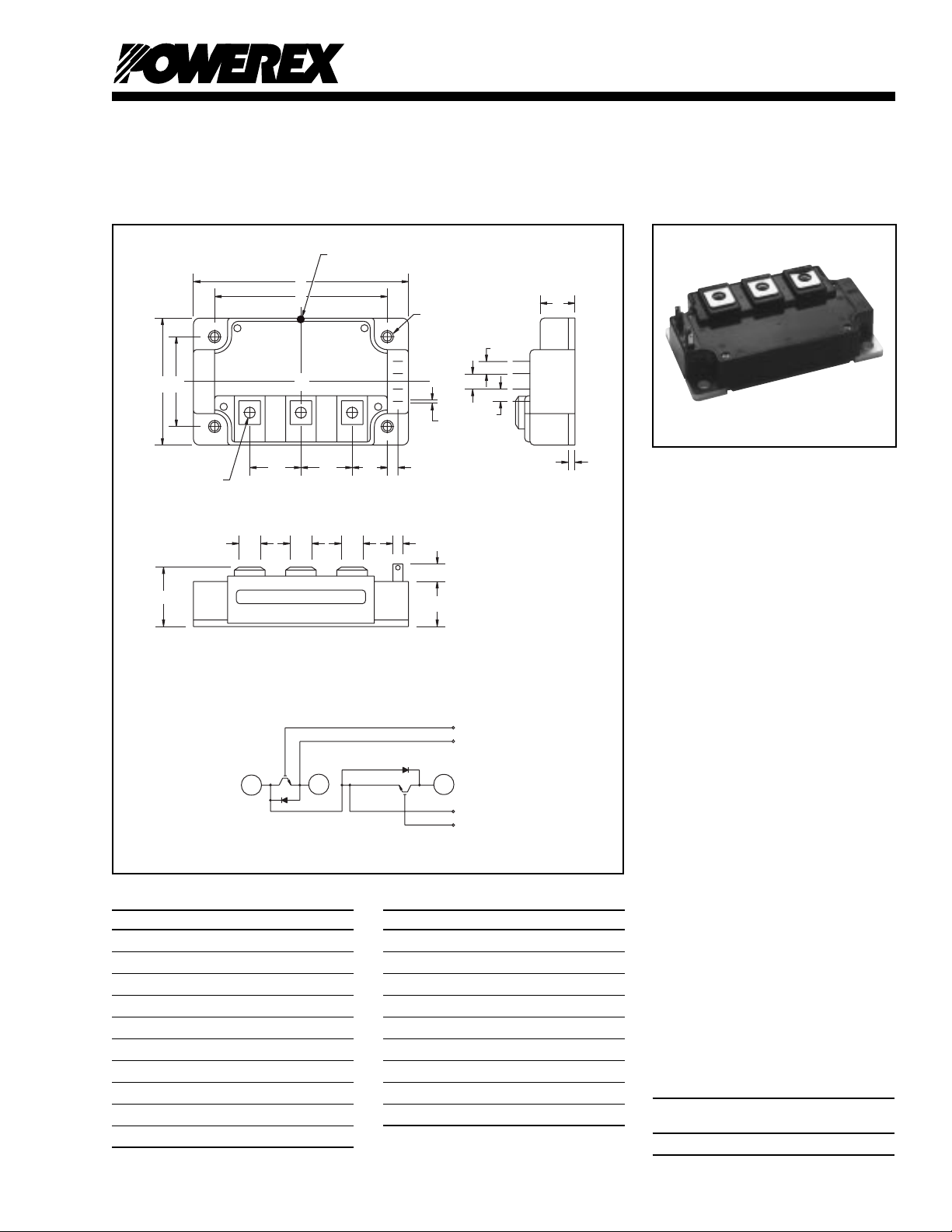
CM400DU-5F
Powerex, Inc., 200 Hillis Street, Youngwood, Pennsylvania 15697-1800 (724) 925-7272
EB
S - NUTS
(3 TYP)
C
CM
C2E1 E2
K
TC MEASURE POINT
A
D
C
L
Q
T - (4 TYP.)
G2
E2
E1
G1
C1
PQ
KK
U
N
R
M
L
H
J
H
F
G
Trench Gate Design
Dual IGBTMOD™
400 Amperes/ 250 Volts
Description:
Powerex IGBTMOD™ Modules
are designed for use in switching
applications. Each module consists
of two IGBT Transistors in a halfbridge configuration with each transistor having a reverse-connected
super-fast recover y free-wheel
diode. All components and interconnects are isolated from the
heat sinking baseplate, offering
simplified system assembly and
thermal management.
C2E1
E2
Outline Drawing and Circuit Diagram
Dimensions Inches Millimeters
A 4.25 108.0
B 2.44 62.0
C 1.14 +0.04/-0.02 29.0 +1.0/-0.5
D 3.66±0.01 93.0±0.25
E 1.88±0.01 48.0±0.25
F 0.67 17.0
G 0.16 4.0
H 0.24 6.0
J 0.59 15.0
K 0.55 14.0
G2
E2
C1
E1
G1
Dimensions Inches Millimeters
L 0.87 22.0
M 0.33 8.5
N 0.10 2.5
P 0.85 21.5
Q 0.98 25.0
R 0.11 2.8
SM6 M6
T 0.26 Dia. 6.5 Dia.
U 0.002 0.05
Features:
□ Low Drive Power
□ Low V
CE(sat)
□ Discrete Super-Fast Recovery
Free-Wheel Diode
□ Isolated Baseplate for Easy
Heat Sinking
Applications:
□ AC Motor Control
□ Motion/Servo Control
□ UPS
□ Welding Power Supplies
□ Laser Power Supplies
Ordering Information:
Example: Select the complete
module number you desire from
the table - i.e. CM400DU-5F is a
250V (V
), 400 Ampere Dual
CES
IGBTMOD™ Power Module.
Current Rating V
Type Amperes Volts (x 50)
CM 400 5
CES
1
1
Page 3

Powerex, Inc., 200 Hillis Street, Youngwood, Pennsylvania 15697-1800 (724) 925-7272
CM400DU-5F
Trench Gate Design Dual IGBTMOD™
400 Amperes/250 Volts
Absolute Maximum Ratings, T
= 25 °C unless otherwise specified
j
Ratings Symbol CM400DU-5F Units
Junction Temperature T
Storage Temperature T
Collector-Emitter Voltage (G-E SHORT) V
Gate-Emitter Voltage (C-E SHORT) V
Collector Current (Tc = 25°C) I
Peak Collector Current (Tj ≤ 150°C) I
Emitter Current** (Tc = 25°C) I
Peak Emitter Current** I
Maximum Collector Dissipation (Tc = 25°C) P
j
stg
CES
GES
C
CM
E
EM
c
-40 to 150 °C
-40 to 125 °C
250 Volts
±20 Volts
400 Amperes
800* Amperes
400 Amperes
800* Amperes
890 Watts
Mounting Torque, M6 Main Terminal – 40 in-lb
Mounting Torque, M6 Mounting – 40 in-lb
Weight – 400 Grams
Isolation Voltage (Main Terminal to Baseplate, AC 1 min.) V
* Pulse width and repetition rate should be such that the device junction temperature (Tj) does not exceed T
**Represents characteristics of the anti-parallel, emitter-to-collector free-wheel diode (FWDi).
Static Electrical Characteristics, T
= 25 °C unless otherwise specified
j
iso
j(max)
2500 Volts
rating.
Characteristics Symbol Test Conditions Min. Typ. Max. Units
Collector-Cutoff Current I
Gate Leakage Current I
Gate-Emitter Threshold Voltage V
Collector-Emitter Saturation Voltage V
CES
GES
GE(th)
CE(sat)
VCE = V
VGE = V
, VGE = 0V – – 1.0 mA
CES
, VCE = 0V – – 0.5 µA
GES
IC = 40mA, VCE = 10V 3.0 4.0 5.0 Volts
IC = 400A, VGE = 10V, Tj = 25°C– 1.2 1.7 Volts
IC = 400A, VGE = 10V, Tj = 125°C– 1.1 – Volts
Total Gate Charge Q
Emitter-Collector Voltage* V
* Pulse width and repetition rate should be such that the device junction temperature (Tj) does not exceed T
Dynamic Electrical Characteristics, T
G
EC
= 25 °C unless otherwise specified
j
VCC = 100V, IC = 400A, VGE = 10V – 1500 – nC
IE = 400A, VGE = 0V – – 2.0 Volts
rating.
j(max)
Characteristics Symbol Test Conditions Min. Typ. Max. Units
Input Capacitance C
Output Capacitance C
Reverse Transfer Capacitance C
Resistive Turn-on Delay Time t
Load Rise Time t
Switch Turn-off Delay Time t
Times Fall Time t
Diode Reverse Recovery Time t
Diode Reverse Recovery Charge Q
ies
oes VCE
res
d(on)
r
d(off)
f
rr
rr
Thermal and Mechanical Characteristics, T
= 10V, V
= 0V – – 7.0 nf
GE
VCC = 100V, IC = 400A, – – 850 ns
V
= V
GE1
= 10V, – – 400 ns
GE2
RG = 6.3⍀, Resistive – – 1100 ns
Load Switching Operation – – 500 ns
IE = 400A – – 300 ns
IE = 400A – 16.0 – µC
= 25 °C unless otherwise specified
j
––110 nf
––3.8 nf
Characteristics Symbol Test Conditions Min. Typ. Max. Units
Thermal Resistance, Junction to Case R
Thermal Resistance, Junction to Case R
Thermal Resistance, Junction to Case R
Contact Thermal Resistance R
* TC measured point is just under chip.
2
2
QPer IGBT 1/2 Module – – 0.14 °C/W
th(j-c)
DPer FWDi 1/2 Module – – 0.24 °C/W
th(j-c)
QPer IGBT 1/2 Module* – – 0.08 °C/W
th(j-c´)
th(c-f)
Per Module, Thermal Grease Applied – 0.04 – °C/W
Page 4

Powerex, Inc., 200 Hillis Street, Youngwood, Pennsylvania 15697-1800 (724) 925-7272
CM400DU-5F
Trench Gate Design Dual IGBTMOD™
400 Amperes/250 Volts
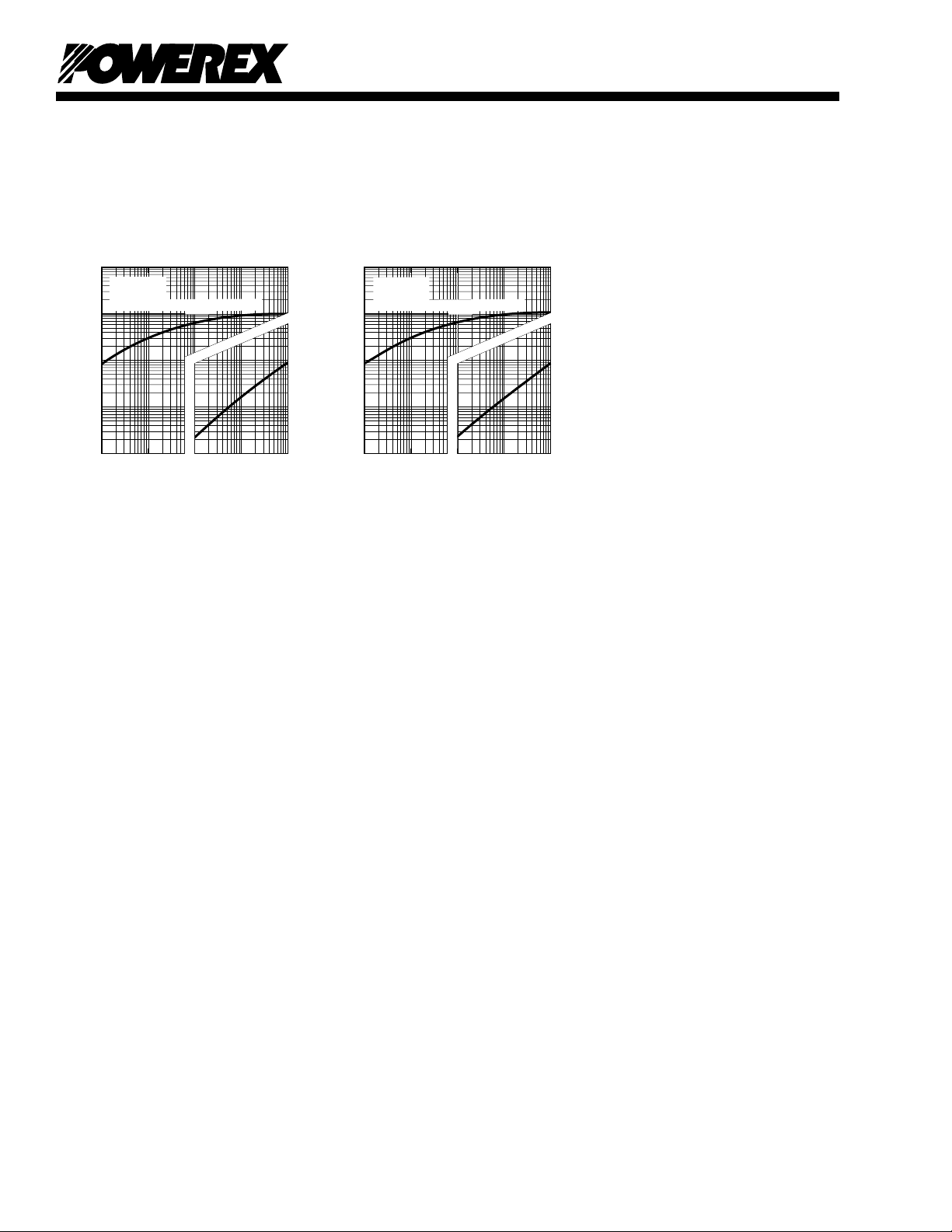
OUTPUT CHARACTERISTICS
(TYPICAL)
800
540
, (AMPERES)
C
480
Tj = 25
VGE = 15V
10
o
C
8
6.25
6.5
6
5.75
320
5.5
160
COLLECTOR CURRENT, I
0
0
12345
COLLECTOR-EMITTER VOLTAGE, VCE, (VOLTS)
SATURATION VOLTAGE CHARACTERISTICS
10
8
, (VOLTS)
CE(sat)
6
4
COLLECTOR-EMITTER
2
SATURATION VOLTAGE, V
0
3
10
2
10
SWITCHING TIME, (ns)
1
10
10
COLLECTOR-EMITTER
(TYPICAL)
Tj = 25°C
IC = 800A
IC = 160A
048121620
GATE-EMITTER VOLTAGE, VGE, (VOLTS)
HALF-BRIDGE
SWITCHING CHARACTERISTICS
1
COLLECTOR CURRENT, IC, (AMPERES)
(TYPICAL)
10
2
5.25
5
IC = 400A
VCC = 100V
V
= ±10V
GE
R
= 6.3 Ω
G
T
= 125°C
j
t
d(off)
t
d(on)
t
f
t
r
COLLECTOR-EMITTER
(TYPICAL)
VGE = 15V
Tj = 25°C
= 125°C
T
j
0 160 320 480 640
COLLECTOR-CURRENT, IC, (AMPERES)
CAPACITANCE VS. V
(TYPICAL)
VGE = 0V
f = 1MHz
-1
COLLECTOR-EMITTER VOLTAGE, VCE, (VOLTS)
0
10
GATE CHARGE, V
CE
C
ies
C
oes
C
res
1
10
GE
IC = 400A
VCC = 50V
VCC = 100V
800
10
2
800
640
, (AMPERES)
C
480
TRANSFER CHARACTERISTICS
VCE = 10V
= 25°C
T
j
= 125°C
T
j
(TYPICAL)
320
160
COLLECTOR CURRENT, I
0
0246810
GATE-EMITTER VOLTAGE, VGE, (VOLTS)
FREE-WHEEL DIODE
FORWARD CHARACTERISTICS
3
10
Tj = 25°C
, (AMPERES)
E
2
10
EMITTER CURRENT, I
1
10
0.6 0.8 1.0 1.2 1.61.4 1.8
EMITTER-COLLECTOR VOLTAGE, V
REVERSE RECOVERY CHARACTERISTICS
3
10
, (ns)
rr
2
10
(TYPICAL)
(TYPICAL)
, (VOLTS)
EC
SATURATION VOLTAGE CHARACTERISTICS
2.0
1.6
, (VOLTS)
CE(sat)
1.2
0.8
COLLECTOR-EMITTER
0.4
SATURATION VOLTAGE, V
0
2
10
, (nF)
res
1
, C
10
oes
, C
ies
0
10
CAPACITANCE, C
-1
10
10
3
10
t
rr
I
rr
10
, (AMPERES)
2
rr
20
16
, (VOLTS)
GE
12
8
VCC = 100V
V
= ±10V
REVERSE RECOVERY TIME, t
1
3
10
10
1
10
EMITTER CURRENT, IE, (AMPERES)
GE
R
= 6.3 Ω
G
T
= 125°C
j
2
10
10
3
10
4
GATE-EMITTER VOLTAGE, V
1
REVERSE RECOVERY CURRENT, I
0
0 500 15001000
GATE CHARGE, QG, (nC)
25002000 3000
3
3
Page 5
Powerex, Inc., 200 Hillis Street, Youngwood, Pennsylvania 15697-1800 (724) 925-7272
CM400DU-5F
Trench Gate Design Dual IGBTMOD™
400 Amperes/250 Volts
TRANSIENT THERMAL
IMPEDANCE CHARACTERISTICS
-3
10
1
th(j-c)
10
Single Pulse
= 25°C
T
C
Per Unit Base = R
0
10
-1
10
• (NORMALIZED VALUE)
th
-2
10
= R
th
Z
-3
10
NORMALIZED TRANSIENT THERMAL IMPEDANCE, Z
(IGBT)
-2
10
-1
10
th(j-c)
-5
10
TIME, (s)
0
10
= 0.14°C/W
-4
10
TRANSIENT THERMAL
IMPEDANCE CHARACTERISTICS
1
10
-1
10
-2
10
-3
10
-3
10
-3
10
1
th(j-c)
10
Single Pulse
= 25°C
T
C
Per Unit Base = R
0
10
-1
10
• (NORMALIZED VALUE)
th
-2
10
= R
th
Z
-3
10
NORMALIZED TRANSIENT THERMAL IMPEDANCE, Z
(FWDi)
-2
10
-1
10
th(j-c)
-5
10
TIME, (s)
10
= 0.24°C/W
-4
10
0
1
10
-1
10
-2
10
-3
10
-3
10
4
4
 Loading...