

Page 1

6121 Baker Road,
Suite 108
Minnetonka, MN 55345
www.chtechnology.com
Phone (952) 933-6190
Fax (952) 933-6223
1-800-274-4284
Thank you for downloading this document from C&H Technology, Inc.
Please contact the C&H Technology team for the following questions -
Technical
Application
Assembly
Availability
Pricing
Phone – 1-800-274-4284
E-Mail – sales@chtechnology.com
www.chtechnology.com - SPECIALISTS IN POWER ELECTRONIC COMPONENTS AND ASSEMBLIES - www.chtechnology.com
Page 2
CM150RX-12A
Powerex, Inc., 173 Pavilion Lane, Youngwood, Pennsylvania 15697 (724) 925-7272
AN
AP
AK
AJ
12
11
10
N M L K B
9
8
7
6
5
AB
(6 PLACES)
DETAIL "B"
TH1
2
TH
(11)
(10)
NTC
*ALL PIN DIMENSIONS WITHIN
A TOLERANCE OF ±0.5
AX
AL
AT
AR
AS
AU
AL
AV
AL
AW
AY
DETAIL "B"
AZ
R
AD
C
AC
BB
DETAIL "A"
AH
AL
AK
AJ
AE
T
S
R
U
V
AF
AG
BC
BD
BE
H
J
QR
P
Q
P
H
X Y Z Z
P(35)
UP(34)
G
E
G
UP(33)
UN(30)
B(4)
GB(6)
EB(5)
N(36)
34 33 32 31 30 29 28 27 26 25 24 23 22 21 20 19 18 17 16 15 14 13
AA(4 PLACES)
35
36
1 2 3 4
J
P W
VP(26)
G
E
VP(25)
U(1) V(2) W(3)
G
VN(22)
ALAL
ALALAL
AMAMAM
AMAM
A
D
E
F
G
DETAIL "A"
RQ
WP(18)
G
E
WP(17)
G
WN(14)
EWN(13)EVN(21)EUN(29)
Z
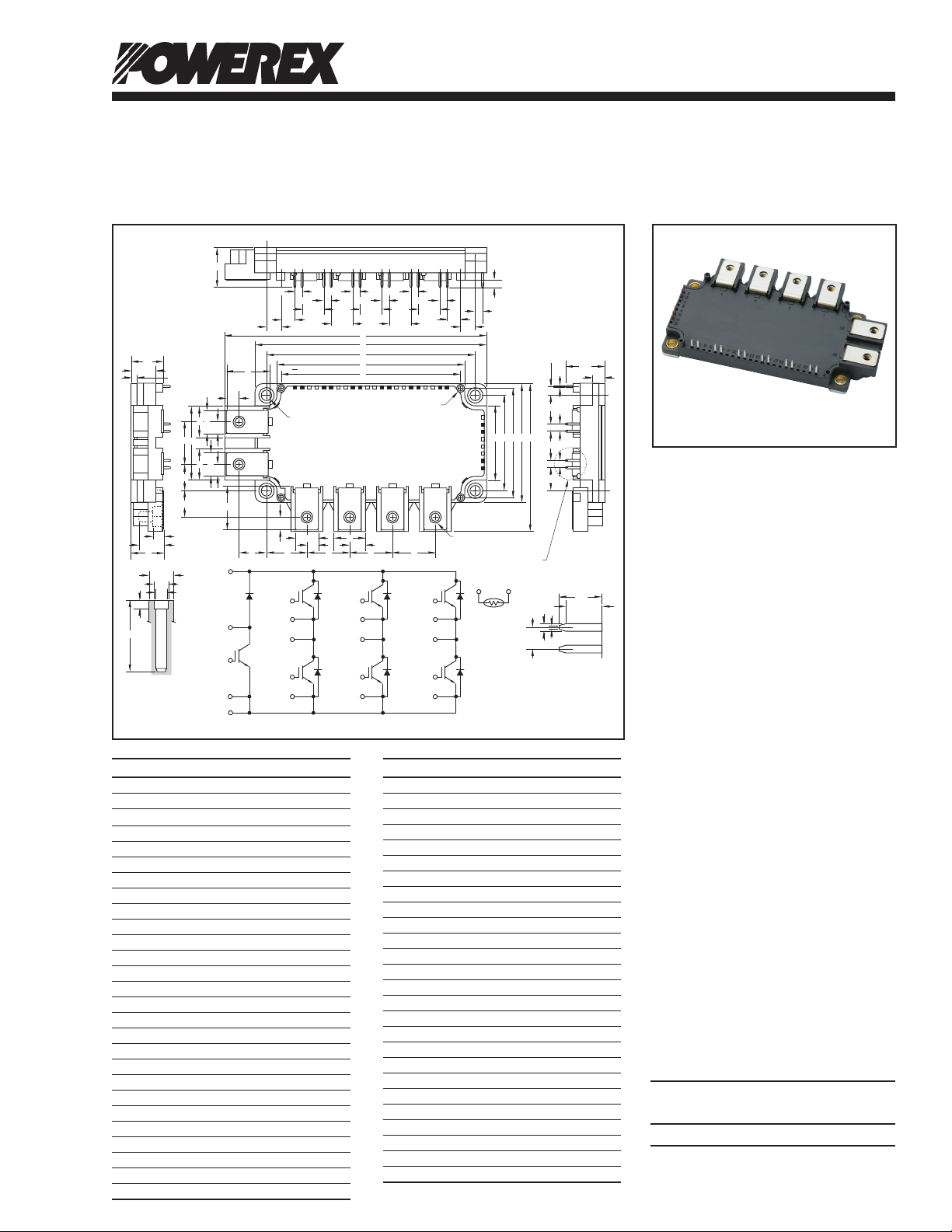
Outline Drawing and Circuit Diagram
Dimensions Inches Millimeters
A 5.39 136.9
B 3.03 77.1
C 0.67+0.04/-0.02 17.0+1.0/-0.5
D 4.79 121.7
E 4.33±0.02 110.0±0.5
F 3.89 99.0
G 3.72 94.5
H 0.83 21.14
J 0.37 6.5
K 2.44 62.0
L 2.26 57.5
M 1.97±0.02 50.0±0.5
N 1.53 39.0
P 0.24 6.0
Q 0.48 12.0
R 0.67 17.0
S 1.53 39.0
T 0.87 22.0
U 0.55 14.0
V 0.54 13.64
W 0.33 8.5
X 0.53 13.5
Y 0.81 20.71
Z 0.9 22.86
AA 0.22 Dia. 5.5 Dia.
AB M5 M5
AC 0.06 1.5
Dimensions Inches Millimeters
AD 0.51 13.0
AE 0.12 3.0
AF 0.21 5.4
AG 0.49 12.5
AH 0.81 20.5
AJ 0.30 7.75
AK 0.28 7.25
AL 0.15 3.81
AM 0.45 11.44
AN 0.14 3.5
AP 0.16 4.06
AQ 0.78 20.05
AR 0.03 0.8
AS 0.27 7.0
AT 0.16 4.2
AU 0.61 15.48
AV 0.60 15.24
AW 0.46 11.66
AX 0.04 1.15
AY 0.02 0.65
AZ 0.29 7.4
BA 0.05 6.2
BB 0.49 12.5
BC 0.17 Dia. 4.3 Dia.
BD 0.10 Dia. 2.5 Dia.
BE 0.08 Dia. 2.1Dia.
Six IGBTMOD™ + Brake
NX-Series Module
150 Amperes/600 Volts
AQ
Description:
Powerex IGBTMOD™ Modules
are designed for use in switching
applications. Each module
consists of six IGBT Transistors in
a three phase bridge configuration
and a seventh IGBT with free-
BA
wheel diode for dynamic braking.
All components and interconnects
are isolated from the heat sinking
baseplate, offering simplified
system assembly and thermal
management.
Features:
£ Low Drive Power
£ Low V
CE(sat)
£ Discrete Super-Fast Recovery
Free-Wheel Diode
£ Isolated Baseplate for Easy
Heat Sinking
Applications:
£ AC Motor Control
£ Motion/Servo Control
£ Photovoltaic/Fuel Cell
Ordering Information:
Example: Select the complete
module number you desire from
the table below -i.e.
CM150RX-12A is a 600V (V
CES
),
150 Ampere Six-IGBTMOD™ +
Brake Power Module.
Type Current Rating
Amperes Volts (x 50)
CM 150 12
V
CES
1Rev. 11/08
Page 3

Powerex, Inc., 173 Pavilion Lane, Youngwood, Pennsylvania 15697 (724) 925-7272
CM150RX-12A
Six IGBTMOD™ + Brake NX-Series Module
150 Amperes/600 Volts
Absolute Maximum Ratings, Tj = 25°C unless otherwise specied
Characteristics Symbol CM150RX-12A Units
Power Device Junction Temperature Tj -40 to 150 °C
Storage Temperature T
-40 to 125 °C
stg
Mounting Torque, M5 Mounting Screws — 31 in-lb
Mounting Torque, M5 Main Terminal Screws — 31 in-lb
Module Weight (Typical) — 330 Grams
Isolation Voltage, AC 1 minute, 60Hz Sinusoidal V
2500 Volts
ISO
Inverter Sector
Collector-Emitter Voltage (G-E Short) V
Gate-Emitter Voltage (C-E Short) V
Collector Current (TC = 63°C)* IC 150 Amperes
Peak Collector Current** ICM 300 Amperes
Emitter Current (TC = 25°C, Tj < 150°C)* IE*** 150 Amperes
Peak Emitter Current (Tj < 150°C)** IEM*** 300 Amperes
Maximum Collector Dissipation (TC = 25°C, Tj < 150°C)* PC 520 Watts
600 Volts
CES
±20 Volts
GES
Brake Sector
Collector-Emitter Voltage (G-E Short) V
Gate-Emitter Voltage (C-E Short) V
Collector Current (TC = 70°C)* IC 75 Amperes
Peak Collector Current** ICM 150 Amperes
Maximum Collector Dissipation (TC = 25°C, Tj < 150°C)* PC 280 Watts
Repetitive Peak Reverse Voltage (Clamp Diode Part) V
Forward Current (TC = 25°C)* IF*** 75 Amperes
Forward Current (Clamp Diode Part)** IFM*** 150 Amperes
*TC, Tf measured point is just under the chips.
**Pulse width and repetition rate should be such that device junction temperature (Tj) does not exceed T
***Represents characteristics of the anti-parallel, emitter-to-collector free-wheel diode (FWDi).
600 Volts
CES
±20 Volts
GES
*** 600 Volts
RRM
rating.
j(max)
2 Rev. 11/08
Page 4

Powerex, Inc., 173 Pavilion Lane, Youngwood, Pennsylvania 15697 (724) 925-7272
Chip Location (Top View)
CM150RX-12A
Six IGBTMOD™ + Brake NX-Series Module
150 Amperes/600 Volts
Electrical and Mechanical Characteristics, Tj = 25°C unless otherwise specied
Inverter Sector
Characteristics Symbol Test Conditions Min. Typ. Max. Units
Collector Cutoff Current I
Gate-Emitter Threshold Voltage V
Gate Leakage Current I
Collector-Emitter Saturation Voltage V
IC = 150A, VGE = 15V, Tj = 125°C — 1.9 — Volts
IC = 150A, VGE = 15V, Chip — 1.6 — Volts
Input Capacitance C
Output Capacitance C
Reverse Transfer Capacitance C
Total Gate Charge QG VCC = 300V, IC = 150A, VGE = 15V — 400 — nC
Inductive Turn-on Delay Time t
Load Turn-on Rise Time tr VCC = 300V, IC = 150A, — — 100 ns
Switch Turn-off Delay Time t
Time Turn-off Fall Time tf RG = 6.2Ω, IE = 150A, — — 600 ns
Reverse Recovery Time* trr Inductive Load Switching Operation — — 200 ns
Reverse Recovery Charge* Qrr — 5.0 — µC
Emitter-Collector Voltage* VEC IE = 150A, VGE = 0V, Tj = 25°C — 2.0 2.8 Volts
IE = 150A, VGE = 0V, Tj = 125°C — 1.95 — Volts
IE = 150A, VGE = 0V, Chip — 1.9 — Volts
VCE = V
CES
IC = 15mA, VCE = 10V 5 6 7 Volts
GE(th)
VGE = V
GES
IC = 150A, VGE = 15V, Tj = 25°C — 1.7 2.1 Volts
CE(sat)
— — 18.0 nF
ies
VCE = 10V, VGE = 0V — — 2.0 nF
oes
— — 0.6 nF
res
— — 120 ns
d(on)
VGE = ±15V, — — 350 ns
d(off)
, VGE = 0V — — 1.0 mA
CES
, VCE = 0V — — 0.5 µA
GES
Thermal and Mechanical Characteristics, Tj = 25°C unless otherwise specied
Characteristics Symbol Test Conditions Min. Typ. Max. Units
Thermal Resistance, Junction to Case** R
Thermal Resistance, Junction to Case** R
Contact Thermal Resistance** R
Internal Gate Resistance R
External Gate Resistance RG 4.1 — 41 Ω
*Represents characteristics of the anti-parallel, emitter-to-collector free-wheel diode (FWDi).
**TC, Tf measured point is just under the chips.
Q Per IGBT — — 0.24 °C/W
th(j-c)
D Per FWDi — — 0.46 °C/W
th(j-c)
Thermal Grease Applied — 0.015 — °C/W
th(c-f)
TC = 25°C — 0 — Ω
Gint
CHIP LOCATION (TOP VIEW)
IGBT FWDi NTC Thermistor
0
22.6
34.1
45.3
55.8
79.6
89.3
79.1
99.7
Br
Th
WNVNUN
WN
Br
97.8
89.6
96.4
0
1 7. 3
12
11
10
26.8
9
8
7
6
41.4
5
20.6
26.0
29.4
35.4
0
34
33 32 31 30 29 28 27 26 25 24 23 22
UP VP WP
35
UP VP WP
36
1 2 3 4
0
23.1
33.6
21 20 19 18 17 16 15 14 13
V
NUN
44.8
55.3
Dimensions in mm (Tolerance: ±1mm)
3Rev. 11/08
Page 5

Powerex, Inc., 173 Pavilion Lane, Youngwood, Pennsylvania 15697 (724) 925-7272
CM150RX-12A
Six IGBTMOD™ + Brake NX-Series Module
150 Amperes/600 Volts
Electrical and Mechanical Characteristics, Tj = 25°C unless otherwise specied
Brake Sector
Characteristics Symbol Test Conditions Min. Typ. Max. Units
Collector Cutoff Current I
Gate-Emitter Threshold Voltage V
Gate Leakage Current I
Collector-Emitter Saturation Voltage V
IC = 75A, VGE = 15V, Tj = 125°C — 1.9 — Volts
IC = 75A, VGE = 15V, Chip — 1.6 — Volts
Input Capacitance C
Output Capacitance C
Reverse Transfer Capacitance C
Total Gate Charge QG VCC = 300V, IC = 75A, VGE = 15V — 200 — nC
Repetitive Reverse Current* I
Forward Voltage Drop * VF IF = 75A, Tj = 25°C — 2.0 2.8 Volts
IF = 75A, Tj = 125°C — 1.95 — Volts
IF = 75A, Chip — 1.9 — Volts
VCE = V
CES
IC = 7.5mA 5 6 7 Volts
GE(th)
VGE = V
GES
IC = 75A, VGE = 15V, Tj = 25°C — 1.7 2.1 Volts
CE(sat)
— — 9.3 nF
ies
VCE = 10V, VGE = 0V — — 1.0 nF
oes
— — 0.3 nF
res
VR = V
RRM
, VGE = 0V — — 1.0 mA
CES
, VCE = 0V — — 0.5 µA
GES
— — 1.0 mA
RRM
Thermal and Mechanical Characteristics, Tj = 25°C unless otherwise specied
Characteristics Symbol Test Conditions Min. Typ. Max. Units
Thermal Resistance, Junction to Case** R
Thermal Resistance, Junction to Case** R
Contact Thermal Resistance** R
Internal Gate Resistance R
Q Per IGBT — — 0.44 °C/W
th(j-c)
D Per FWDi — — 0.85 °C/W
th(j-c)
Thermal Grease Applied — 0.015 — °C/W
th(j-f)
TC = 25°C — 0 — Ω
Gint
External Gate Resistance RG 8 — 83 Ω
NTC Thermistor Sector, Tj = 25°C unless otherwise specied
Characteristics Symbol Test Conditions Min. Typ. Max. Units
Zero Power Resistance R TC = 25°C 4.85 5.00 5.15 kΩ
Deviation of Resistance ∆R/R TC = 100°C, R
B Constant B
B = (InR1 – InR2) / (1/T1 – 1/T2)*** — 3375 — K
(25/50)
Power Dissipation P25 TC = 25°C — — 10 mW
*Represents characteristics of the anti-parallel, emitter-to-collector free-wheel diode (FWDi).
**TC, Tf measured point is just under the chips.
***R1: Resistance at Absolute Temperature T1(K), R2: Resistance at Absolute Temperature T2(K), T(K) = t(°C) + 273.15
= 493Ω –7.3 — +7.8 %
100
4 Rev. 11/08
Page 6

Powerex, Inc., 173 Pavilion Lane, Youngwood, Pennsylvania 15697 (724) 925-7272
CM150RX-12A
Six IGBTMOD™ + Brake NX-Series Module
150 Amperes/600 Volts
OUTPUT CHARACTERISTICS
(INVERTER PART - TYPICAL)
300
VGE = 20V
13
250
15
200
, (AMPERES)
C
150
100
50
COLLECTOR CURRENT, I
0
0 2 4 6 8 10
COLLECTOR-EMITTER VOLTAGE, VCE, (VOLTS)
FREE-WHEEL DIODE
FORWARD CHARACTERISTICS
(INVERTER PART - TYPICAL)
3
10
, (AMPERES)
E
10
EMITTER CURRENT, I
10
10
10
SWITCHING TIME, (ns)
10
Tj = 25°C
= 125°C
T
j
2
1
0 1 32 4
EMITTER-COLLECTOR VOLTAGE, V
SWITCHING TIME VS.
GATE RESISTANCE
(INVERTER PART - TYPICAL)
3
t
f
t
2
1
d(off)
t
d(on)
t
r
0
10
GATE RESISTANCE, R
1
10
Tj = 25°C
12
11
10
8
9
, (VOLTS)
EC
VCC = 300V
V
= ±15V
GE
I
= 150A
C
T
= 125°C
j
Inductive Load
, (Ω)
G
SATURATION VOLTAGE CHARACTERISTICS
3.5
3.0
, (VOLTS)
2.5
CE(sat)
2.0
COLLECTOR-EMITTER
(INVERTER PART - TYPICAL)
VGE = 15V
Tj = 25°C
= 125°C
T
j
1.5
COLLECTOR-EMITTER
1.0
0.5
SATURATION VOLTAGE, V
0
0
COLLECTOR-CURRENT, IC, (AMPERES)
CAPACITANCE VS. V
(INVERTER PART - TYPICAL)
2
10
VGE = 0V
, (nF)
res
1
10
, C
oes
, C
ies
0
10
CAPACITANCE, C
-1
10
-1
10
COLLECTOR-EMITTER VOLTAGE, VCE, (VOLTS)
REVERSE RECOVERY CHARACTERISTICS
3
10
VCC = 300V
V
GE
R
2
10
G
T
= 25°C
j
Inductive Load
(ns)
rr
(A), t
rr
0
10
10
(INVERTER PART - TYPICAL)
= ±15V
= 6.2Ω
SATURATION VOLTAGE CHARACTERISTICS
10
8
, (VOLTS)
CE(sat)
6
4
COLLECTOR-EMITTER
2
SATURATION VOLTAGE, V
300100 200
0
CE
3
10
C
ies
2
10
C
oes
SWITCHING TIME, (ns)
C
res
1
1
2
10
10
10
20
16
, (VOLTS)
GE
12
COLLECTOR-EMITTER
(INVERTER PART - TYPICAL)
Tj = 25°C
IC = 300A
IC = 150A
IC = 60A
6 8 10 1412 16 18 20
GATE-EMITTER VOLTAGE, VGE, (VOLTS)
HALF-BRIDGE
SWITCHING CHARACTERISTICS
(INVERTER PART - TYPICAL)
t
d(off)
t
d(on)
t
r
1
COLLECTOR CURRENT, IC, (AMPERES)
GATE CHARGE VS. V
(INVERTER PART)
2
10
t
f
VCC = 300V
V
GE
R
= 6.2Ω
G
T
= 125°C
j
Inductive Load
GE
= ±15V
10
IC = 150A
VCC = 200V
VCC = 300V
3
8
REVERSE RECOVERY, I
1
2
10
10
1
10
EMITTER CURRENT, IE, (AMPERES)
2
10
I
rr
t
rr
3
10
4
GATE-EMITTER VOLTAGE, V
0
100 200 300 600500400
0
GATE CHARGE, QG, (nC)
5Rev. 11/08
Page 7

Powerex, Inc., 173 Pavilion Lane, Youngwood, Pennsylvania 15697 (724) 925-7272
CM150RX-12A
Six IGBTMOD™ + Brake NX-Series Module
150 Amperes/600 Volts
SWITCHING LOSS VS.
COLLECTOR CURRENT
(INVERTER PART - TYPICAL)
1
10
, (mJ/PULSE)
off
, E
on
0
10
VCC = 300V
V
R
T
Inductive Load
SWITCHING LOSS, E
-1
10
0
10
COLLECTOR CURRENT, IC, (AMPERES)
REVERSE RECOVERY SWITCHING LOSS VS.
2
10
1
10
, (mJ/PULSE)
rr
0
10
REVERSE RECOVERY
SWITCHING LOSS, E
-1
10
10
3
10
GATE RESISTANCE
(INVERTER PART - TYPICAL)
VCC = 300V
V
= ±15V
GE
I
= 150A
E
T
= 125°C
j
Inductive Load
0
GATE RESISTANCE, R
FREE-WHEEL DIODE
FORWARD CHARACTERISTICS
(BRAKE PART - TYPICAL)
Tj = 25°C
= 125°C
T
j
1
10
1
10
= ±15V
GE
= 6.2Ω
G
= 125°C
j
E
E
E
rr
, (Ω)
G
SWITCHING LOSS VS.
GATE RESISTANCE
(INVERTER PART - TYPICAL)
2
10
1
10
, (mJ/PULSE)
off
, E
on
0
10
on
off
2
10
2
10
SWITCHING LOSS, E
-1
10
0
10
10-310
0
th(j-c')
10
-1
10
• (NORMALIZED VALUE)
-2
10
th
= R
th
Z
-3
10
NORMALIZED TRANSIENT THERMAL IMPEDANCE, Z
10-310
0
th(j-c')
10
GATE RESISTANCE, RG, (Ω)
TRANSIENT THERMAL
IMPEDANCE CHARACTERISTICS
(INVERTER PART - TYPICAL)
-2
Single Pulse
T
= 25°C
C
Per Unit Base =
R
=
th(j-c)
0.24°C/W
(IGBT)
R
=
th(j-c)
0.46°C/W
(FWDi)
TRANSIENT THERMAL
IMPEDANCE CHARACTERISTICS
(BRAKE PART - TYPICAL)
-2
10
-1
10
-5
10
TIME, (s)
-1
10
VCC = 300V
V
I
C
T
Inductive Load
1
= ±15V
GE
= 150A
= 125°C
j
E
E
0
10
-4
10
0
10
on
off
2
10
1
10
-1
10
-2
10
-3
10
-3
10
1
10
REVERSE RECOVERY SWITCHING LOSS VS.
1
10
, (mJ/PULSE)
rr
0
10
REVERSE RECOVERY
SWITCHING LOSS, E
-1
10
10
SATURATION VOLTAGE CHARACTERISTICS
3.5
3.0
, (VOLTS)
2.5
CE(sat)
2.0
EMITTER CURRENT
(INVERTER PART - TYPICAL)
VCC = 300V
V
= ±15V
GE
R
= 6.2Ω
G
T
= 125°C
j
Inductive Load
1
EMITTER CURRENT, IE, (AMPERES)
2
10
COLLECTOR-EMITTER
(BRAKE PART - TYPICAL)
VGE = 15V
Tj = 25°C
= 125°C
T
j
E
rr
1.5
COLLECTOR-EMITTER
1.0
0.5
SATURATION VOLTAGE, V
0
0
COLLECTOR-CURRENT, IC, (AMPERES)
3
10
15050 100
2
10
, (AMPERES)
F
1
10
FORWARD CURRENT, I
0
10
0 1 32 4
FORWARD VOLTAGE, V
, (VOLTS)
F
-1
10
Single Pulse
T
= 25°C
C
Per Unit Base =
R
=
th(j-c)
• (NORMALIZED VALUE)
0.44°C/W
-2
10
th
(IGBT)
= R
th
R
=
th(j-c)
Z
0.85°C/W
(FWDi)
-3
10
NORMALIZED TRANSIENT THERMAL IMPEDANCE, Z
-5
10
TIME, (s)
-4
10
-1
10
-2
10
-3
10
-3
10
6 Rev. 11/08
 Loading...