

Page 1
6121 Baker Road,
Suite 108
Minnetonka, MN 55345
www.chtechnology.com
Phone (952) 933-6190
Fax (952) 933-6223
1-800-274-4284
Thank you for downloading this document from C&H Technology, Inc.
Please contact the C&H Technology team for the following questions -
Technical ● Application ● Assembly ● Availability ● Pricing
Phone – 1-800-274-4284
E-Mail – sales@chtechnology.com
www.chtechnology.com - SPECIALISTS IN POWER ELECTRONIC COMPONENTS AND ASSEMBLIES
-
www.chtechnology.com
Page 2
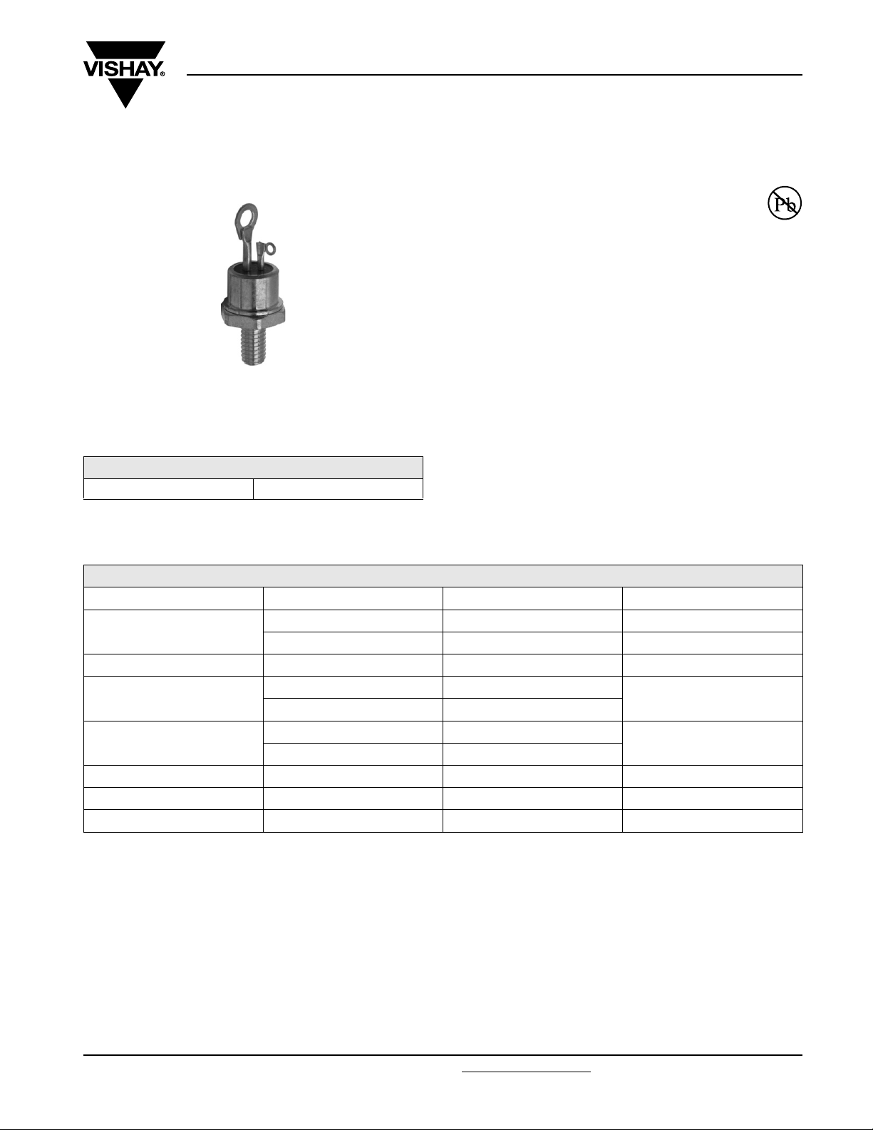
TO-208AA (TO-48)
Vishay High Power Products
Medium Power Thyristors
(Stud Version), 25 A
FEATURES
• Improved glass passivation for high reliability
and exceptional stability at high temperature
• High dI/dt and dV/dt capabilities
• Standard package
• Low thermal resistance
• Metric threads version available
• Types up to 1200 V V
• RoHS compliant
• Designed and qualified for industrial and consumer level
TYPICAL APPLICATIONS
25RIA Series
RoHS
COMPLIANT
DRM/VRRM
PRODUCT SUMMARY
I
T(AV)
25 A
• Medium power switching
• Phase control applications
• Can be supplied to meet stringent military, aerospace and
other high reliability requirements
MAJOR RATINGS AND CHARACTERISTICS
PARAMETER TEST CONDITIONS VALUES UNITS
I
T(AV)
I
T(RMS)
I
TSM
2
I
t
V
DRM/VRRM
t
q
T
J
T
C
50 Hz 420
60 Hz 440
50 Hz 867
60 Hz 790
Typical 110 µs
25 A
85 °C
40 A
A
A2s
100 to 1200 V
- 65 to 125 °C
Document Number: 93701 For technical questions, contact: ind-modules@vishay.com
Revision: 19-Sep-08 1
www.vishay.com
Page 3
25RIA Series
Vishay High Power Products
Medium Power Thyristors
(Stud Version), 25 A
ELECTRICAL SPECIFICATIONS
VOLTAGE RATINGS
TYPE
NUMBER
VOLTAGE
CODE
V
DRM/VRRM
, MAXIMUM REPETITIVE PEAK
AND OFF-STATE VOLTAGE
V
(1)
10 100 150
20 200 300
40 400 500
25RIA
60 600 700
80 800 900
100 1000 1100
120 1200 1300
Notes
(1)
Units may be broken over non-repetitively in the off-state direction without damage, if dI/dt does not exceed 20 A/µs
(2)
For voltage pulses with tp ≤ 5 ms
ABSOLUTE MAXIMUM RATINGS
PARAMETER SYMBOL TEST CONDITIONS VALUES UNITS
Maximum average on-state current
at case temperature
Maximum RMS on-state current I
Maximum peak, one-cycle
non-repetitive surge current
2
Maximum I
Maximum I
t for fusing I2t
2
√t for fusing I2√t
Low level value of threshold voltage V
High level value of threshold voltage V
Low level value of
on-state slope resistance
High level value of
on-state slope resistance
Maximum on-state voltage V
Maximum holding current I
Latching current I
I
T(AV)
T(RMS)
I
TSM
180° sinusoidal conduction
40 A
t = 10 ms
t = 8.3 ms 440
t = 10 ms
t = 8.3 ms 370
t = 10 ms
t = 8.3 ms 790
t = 10 ms
t = 8.3 ms 560
No voltage
reapplied
100 % V
reapplied
No voltage
reapplied
100 % V
reapplied
t = 0.1 to 10 ms, no voltage reapplied,
= TJ maximum
T
J
T(TO)1
T(TO)2
r
t1
r
t2
TM
H
L
(16.7 % x π x I
T
= TJ maximum
J
(I > π x I
(16.7 % x π x I
T
= TJ maximum
J
(I > π x I
Ipk = 79 A, TJ = 25 °C 1.70 V
TJ = 25 °C, anode supply 6 V, resistive load
T(AV)
), TJ = TJ maximum 1.40
T(AV)
T(AV)
), TJ = TJ maximum 5.7
T(AV)
V
RRM
RRM
< I < π x I
< I < π x I
, MAXIMUM NON-REPETITIVE
RSM
PEAK VOLTAGE
(2)
V
Sinusoidal
half wave,
initial T
=
J
maximum
T
J
),
T(AV)
),
T(AV)
I
DRM/IRRM
AT T
= TJ MAXIMUM
J
mA
20
10
25 A
85 °C
420
350
867
615
8670 A
0.99
10.1
130
200
MAXIMUM
A
A
2
V
mΩ
mA
2
s
√s
www.vishay.com For technical questions, contact: ind-modules@vishay.com
Document Number: 93701
2 Revision: 19-Sep-08
Page 4
25RIA Series
Medium Power Thyristors
Vishay High Power Products
(Stud Version), 25 A
SWITCHING
PARAMETER SYMBOL TEST CONDITIONS VALUES UNITS
V
≤ 600 V
DRM
≤ 800 V 180
V
Maximum rate of rise
of turned-on current
DRM
V
≤ 1000 V 160
DRM
≤ 1600 V 150
V
DRM
Typical turn-on time t
Typical reverse recovery time t
Typical turn-off time t
dI/dt
gt
rr
q
= TJ maximum, VDM = Rated V
T
J
DRM
Gate pulse = 20 V, 15 Ω, tp = 6 µs, tr = 0.1 µs maximum
= (2 x rated dI/dt) A
I
TM
TJ = 25 °C,
at rated V
DRM/VRRM
, TJ = 125 °C
TJ = TJ maximum,
I
= I
TM
TJ = TJ maximum, ITM = I
dI/dt = - 10 A/µs, dV/dt = 20 V/µs linear to 67 % V
, tp > 200 µs, dI/dt = - 10 A/µs
T(AV)
T(AV)
, tp > 200 µs, VR = 100 V,
DRM
gate bias 0 V to 100 W
Note
= 10 µs up to 600 V, tq = 30 µs up to 1600 V available on special request
•t
q
BLOCKING
PARAMETER SYMBOL TEST CONDITIONS VALUES UNITS
= TJ maximum linear to 100 % rated V
T
Maximum critical rate of rise
of off-state voltage
dV/dt
J
= TJ maximum linear to 67 % rated V
T
J
Note
(1)
Available with: dV/dt = 1000 V/µs, to complete code add S90 i.e. 25RIA120S90
DRM
DRM
200
0.9
4
,
110
100
(1)
300
A/µs
µs
V/µs
TRIGGERING
PARAMETER SYMBOL TEST CONDITIONS VALUES UNITS
Maximum peak gate power P
Maximum average gate power P
Maximum peak positive gate current I
Maximum peak negative gate voltage -V
DC gate current required to trigger I
DC gate voltage required to trigger V
DC gate current not to trigger I
DC gate voltage not to trigger V
GM
G(AV)
GM
GM
GT
GT
GD
GD
TJ = TJ maximum
TJ = TJ maximum 1.5 A
TJ = TJ maximum 10 V
TJ = - 65 °C
= 25 °C 60
J
= 125 °C 35
T
J
Maximum required gate trigger
current/voltage are the lowest
value which will trigger all units
6 V anode to cathode applied
TJ = - 65 °C 3.0
= 25 °C 2.0
T
J
T
= 125 °C 1.0
J
TJ = TJ maximum, V
= Rated value 2.0 mA
DRM
Maximum gate current/voltage
TJ = TJ maximum,
V
= Rated value
DRM
not to trigger is the maximum
value which will not trigger any
unit with rated V
anode to
DRM
cathode applied
8.0
2.0
90
mAT
0.2 V
W
V
Document Number: 93701 For technical questions, contact: ind-modules@vishay.com
www.vishay.com
Revision: 19-Sep-08 3
Page 5
25RIA Series
Vishay High Power Products
Medium Power Thyristors
(Stud Version), 25 A
THERMAL AND MECHANICAL SPECIFICATIONS
PARAMETER SYMBOL TEST CONDITIONS VALUES UNITS
Maximum operating junction
and storage temperature range
Maximum thermal resistance,
junction to case
Maximum thermal resistance,
case to heatsink
Allowable mounting torque
Approximate weight
Case style See dimensions - link at the end of datasheet TO-208AA (TO-48)
ΔR
CONDUCTION
thJC
CONDUCTION ANGLE SINUSOIDAL CONDUCTION RECTANGULAR CONDUCTION TEST CONDITIONS UNITS
180°
120°
90°
60°
30°
Note
• The table above shows the increment of thermal resistance R
T
, T
J
Stg
R
R
thJC
thCS
DC operation 0.75
Mounting surface, smooth, flat and greased 0.35
Non-lubricated threads
Lubricated threads
0.17 0.13
0.21 0.22
0.27 0.30
0.40 0.42
0.69 0.70
when devices operate at different conduction angles than DC
thJC
- 65 to 125 °C
+ 0 - 10 %
3.4
(30)
+ 0 - 10 %
23
(20)
14 g
0.49 oz.
= TJ maximum K/W
T
J
(lbf ⋅ in)
K/W
N · m
130
120
110
100
90
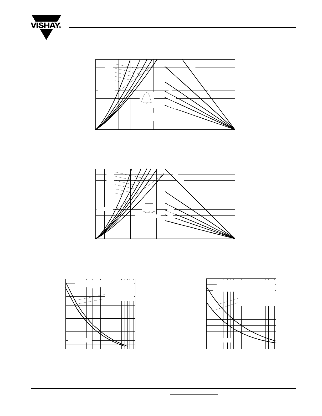
Maximum Allowable Case Temperature (°C)
80
0 5 10 15 20 25 30
25RIA Seri es
R (DC) = 0.75 K/W
thJC
Conducti on Angle
30°
60°
90°
120°
Average On-state Current (A)
180°
130
120
110
100
90
Maximum Allowable Case Temperature (°C)
80
010203040
25RIA Series
R (DC) = 0.75 K/W
thJC
Conducti on Period
30°
60°
90°
120°
180°
Average On-state Current (A)
DC
Fig. 1 - Current Ratings Characteristics Fig. 2 - Current Ratings Characteristics
www.vishay.com For technical questions, contact: ind-modules@vishay.com
Document Number: 93701
4 Revision: 19-Sep-08
Page 6
25RIA Series
Medium Power Thyristors
(Stud Version), 25 A
45
180°
40
120°
35
30
25
20
15
10
Maxi mum Ave rag e On- sta te P owe r Lo ss (W)
60
55
50
45
40
35
30
25
20
15
10
Maximum Average On-state Power Loss (W)
90°
60°
30°
RMS Limit
Conducti on Angle
25RIA Series
T = 125°C
5
0
0 5 10 15 20 25 30
J
Average On-state Current (A)
Fig. 3 - On-State Power Loss Characteristics
DC
180°
120°
90°
60°
30°
RMS Li mi t
Conductio n Period
25RIA Seri es
T = 125°C
J
5
0
0 5 10 15 20 25 30 35 40
Average On-state Current (A)
Fig. 4 - On-State Power Loss Characteristics
Vishay High Power Products
R
t
h
S
2
K
/
3
K
/
W
4
K
/
W
5
K
/
W
7
K
/
W
0 255075100125
Maxi mu m All owabl e Amb ient Tempe ratur e (° C)
R = 1 K/W- D
t
h
2
K
/
W
3
K
/
W
4
K
/
W
5
K
/
W
7
K
/
W
0255075100125
Maximum Allowable Ambient Temperature (°C)
A
=
W
S
A
1
K
/
W
D
e
l
t
a
R
elt
aR
375
350
325
At Any Rated Load Condition And With
Rated V Applied Following Surge.
RRM
Initial T = 125°C
J
@ 60 Hz 0.0083 s
@ 50 Hz 0.0100 s
300
275
250
225
25RI A Ser i es
200
Peak Half Sine Wave On-state Current (A)
175
110100
Number Of Equal Ampli tude Half Cycl e Current Pulses (N)
Fig. 5 - Maximum Non-Repetitive Surge Current
450
Max i mum Non Repet it iv e Surge Cur ren t
425
400
375
350
325
Versus Pulse Train Duration. Control
Of Conduction May Not Be Maintained.
Initial T = 125°C
J
No Voltage Reapplied
Rated V Reapplied
RRM
300
275
250
225
200
25RIA Series
175
Peak Hal f Sin e Wav e On-st ate Current (A)
150
0.01 0.1 1
Pulse Train Duration (s)
Fig. 6 - Maximum Non-Repetitive Surge Current
Document Number: 93701 For technical questions, contact: ind-modules@vishay.com
www.vishay.com
Revision: 19-Sep-08 5
Page 7

25RIA Series
Vishay High Power Products
1000
100
Instantaneous On-state Current (A)
1
Steady State Value
R = 0.75 K/W
thJC
thJC
(DC Operation)
Medium Power Thyristors
(Stud Version), 25 A
25RIA Series
10
1
0.5 1 1.5 2 2.5
Instantaneous On-state Voltage (V)
Fig. 7 - Forward Voltage Drop Characteristics
T = 25°C
J
T = 125°C
J
0.1
25RIA Series
Transient Thermal Impedance Z (K/W)
0.0 1
0.001 0.01 0. 1 1 10
Square Wave Pulse Durati on (s)
Fig. 8 - Thermal Impedance Z
100
Rectangular gate pul se
a) Recommended load line for
rated di/dt : 10V, 20ohms
tr <=0.5 µs, t p >= 6 µs
b) Recommended load line for
<=30% rated di/dt : 10V, 65ohms
10
tr<=1 µs, tp >= 6 µs
(b)
Tj = 25 °C
1
VGD
Instantaneous Gate Voltage (V)
0.1
IGD
0.001 0.01 0.1 1 10 100
Tj = 125 °C
Instantaneous Gate Current (A)
(a)
Tj = -65 °C
25RIA Series Frequency Limited by PG(AV)
Characteristics
thJC
(1) PGM = 16W, tp = 4ms
(2) PGM = 30W, tp = 2ms
(3) PGM = 60W, tp = 1ms
(4) PGM = 60W, tp = 1ms
(1)
Fig. 9 - Gate Characteristics
(2)
(3)
(4)
www.vishay.com For technical questions, contact: ind-modules@vishay.com
Document Number: 93701
6 Revision: 19-Sep-08
Page 8
25RIA Series
Medium Power Thyristors
Vishay High Power Products
(Stud Version), 25 A
ORDERING INFORMATION TABLE
Device code
Dimensions http://www.vishay.com/doc?95333
25 RIA 120 M S90
51324
1 - Current code
- Essential part number
2
- Voltage code x 10 = V
3
- None = Stud base TO-208AA (TO-48) 1/4" 28UNF-2A
4
M = Stud base TO-208AA (TO-48) M6 x 1
- Critical dV/dt:
5
None = 300 V/µs (standard value)
S90 = 1000 V/µs (special selection)
LINKS TO RELATED DOCUMENTS
(see Voltage Ratings table)
RRM
Document Number: 93701 For technical questions, contact: ind-modules@vishay.com
Revision: 19-Sep-08 7
www.vishay.com
Page 9

Legal Disclaimer Notice
Vishay
Disclaimer
ALL PRODUCT, PRODUCT SPECIFICATIONS AND DATA ARE SUBJECT TO CHANGE WITHOUT NOTICE TO IMPROVE
RELIABILITY, FUNCTION OR DESIGN OR OTHERWISE.
Vishay Intertechnology, Inc., its affiliates, agents, and employees, and all persons acting on its or their behalf (collectively,
“Vishay”), disclaim any and all liability for any errors, inaccuracies or incompleteness contained in any datasheet or in any other
disclosure relating to any product.
Vishay makes no warranty, representation or guarantee regarding the suitability of the products for any particular purpose or
the continuing production of any product. To the maximum extent permitted by applicable law, Vishay disclaims (i) any and all
liability arising out of the application or use of any product, (ii) any and all liability, including without limitation special,
consequential or incidental damages, and (iii) any and all implied warranties, including warranties of fitness for particular
purpose, non-infringement and merchantability.
Statements regarding the suitability of products for certain types of applications are based on Vishay’s knowledge of typical
requirements that are often placed on Vishay products in generic applications. Such statements are not binding statements
about the suitability of products for a particular application. It is the customer’s responsibility to validate that a particular
product with the properties described in the product specification is suitable for use in a particular application. Parameters
provided in datasheets and/or specifications may vary in different applications and performance may vary over time. All
operating parameters, including typical parameters, must be validated for each customer application by the customer’s
technical experts. Product specifications do not expand or otherwise modify Vishay’s terms and conditions of purchase,
including but not limited to the warranty expressed therein.
Except as expressly indicated in writing, Vishay products are not designed for use in medical, life-saving, or life-sustaining
applications or for any other application in which the failure of the Vishay product could result in personal injury or death.
Customers using or selling Vishay products not expressly indicated for use in such applications do so at their own risk and agree
to fully indemnify and hold Vishay and its distributors harmless from and against any and all claims, liabilities, expenses and
damages arising or resulting in connection with such use or sale, including attorneys fees, even if such claim alleges that Vishay
or its distributor was negligent regarding the design or manufacture of the part. Please contact authorized Vishay personnel to
obtain written terms and conditions regarding products designed for such applications.
No license, express or implied, by estoppel or otherwise, to any intellectual property rights is granted by this document or by
any conduct of Vishay. Product names and markings noted herein may be trademarks of their respective owners.
Document Number: 91000 www.vishay.com
Revision: 11-Mar-11 1
 Loading...