

Page 1

6121 Baker Road,
Suite 108
Minnetonka, MN 55345
www.chtechnology.com
Phone (952) 933-6190
Fax (952) 933-6223
1-800-274-4284
Thank you for downloading this document from C&H Technology, Inc.
Please contact the C&H Technology team for the following questions -
Technical
Application
Assembly
Availability
Pricing
Phone – 1-800-274-4284
E-Mail – sales@chtechnology.com
www.chtechnology.com - SPECIALISTS IN POWER ELECTRONIC COMPONENTS AND ASSEMBLIES - www.chtechnology.com
Page 2
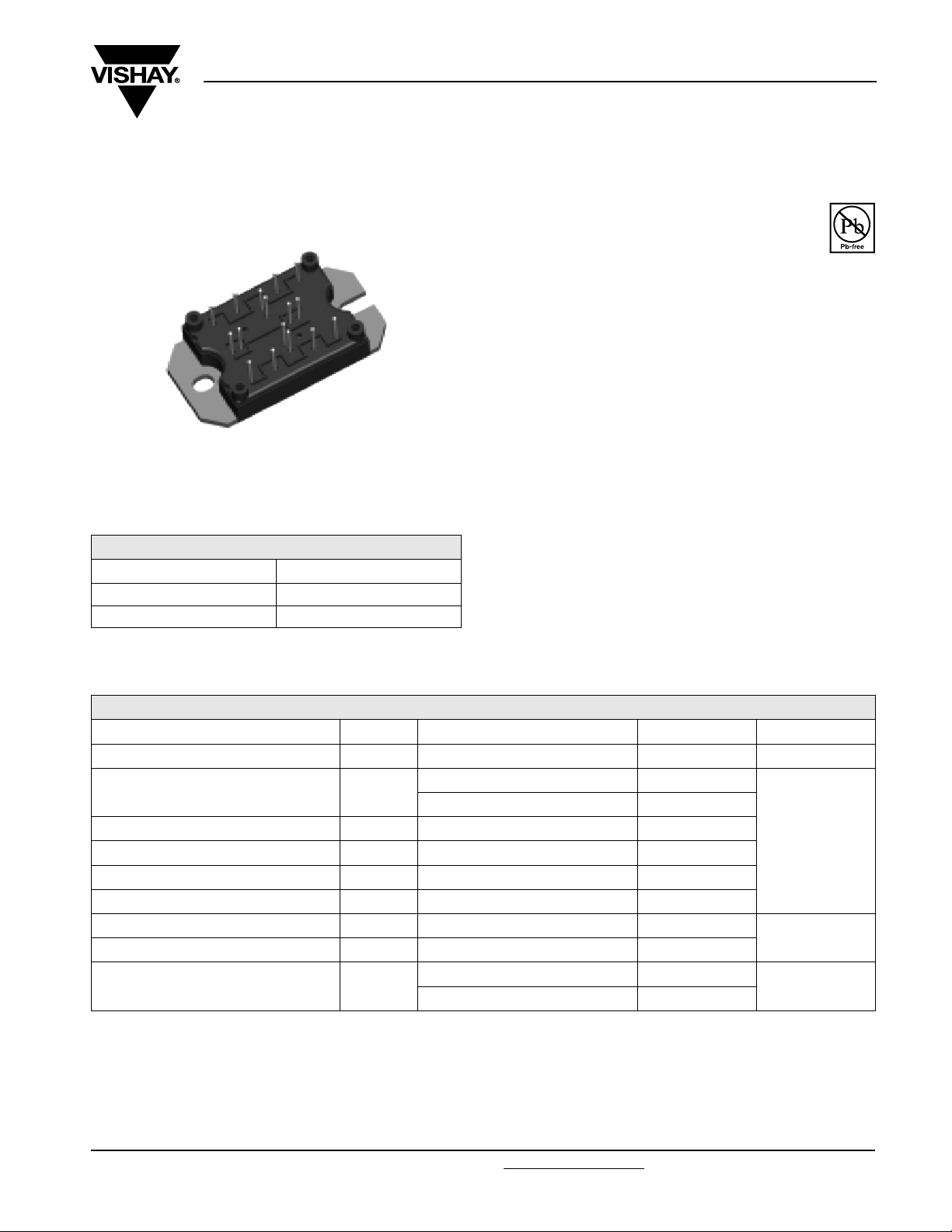
MTP
Vishay High Power Products
"Full-Bridge" IGBT MTP
(Warp Speed IGBT), 50 A
FEATURES
• Generation 4 warp speed IGBT technology
• HEXFRED
reverse recovery
• Very low conduction and switching losses
• Optional SMT thermistor
•Al
2O3
• Very low stray inductance design for high speed operation
• UL pending
• Operating frequencies 8 to 60 kHz > 20 kHz hard
switching, > 200 kHz resonant mode
• Totally lead (Pb)-free
• Designed and qualified for industrial level
®
antiparallel diodes with ultrasoft
DBC
25MT060WFAPbF
RoHS
COMPLIANT
PRODUCT SUMMARY
V
CES
DC 69 A
I
C
V
at 25 A, 25 °C 2.22 V
CE(on)
600 V
• Optimized for welding, UPS and SMPS applications
• Low EMI, requires less snubbing
• Direct mounting to heatsink
• PCB solderable terminals
• Very low junction to case thermal resistance
ABSOLUTE MAXIMUM RATINGS
PARAMETER SYMBOL TEST CONDITIONS MAX. UNITS
BENEFITS
Collector to emitter voltage V
Continuous collector current I
Pulsed collector current I
Peak switching current I
Diode continuous forward current I
Peak diode forward current I
Gate to emitter voltage V
RMS isolation voltage V
Maximum power dissipation
per single IGBT
CES
C
CM
LM
F
FM
GE
ISOL
P
D
TC = 25 °C 69
= 80 °C 46
T
C
TC = 100 °C 25
Any terminal to case, t = 1 min 2500
TC = 25 °C 195
T
= 100 °C 78
C
600 V
200
200
200
± 20
A
V
W
Document Number: 94539 For technical questions, contact: ind-modules@vishay.com
Revision: 30-May-08 1
www.vishay.com
Page 3
25MT060WFAPbF
Vishay High Power Products
"Full-Bridge" IGBT MTP
(Warp Speed IGBT), 50 A
ELECTRICAL SPECIFICATIONS (TJ = 25 °C unless otherwise noted)
PARAMETER SYMBOL TEST CONDITIONS MIN. TYP. MAX. UNITS
Collector to emitter breakdown voltage V
Temperature coefficient of breakdown voltage ΔV
Collector to emitter saturation voltage V
Gate threshold voltage V
Temperature coefficient of threshold voltage ΔV
Transconductance g
Zero gate voltage collector current I
Gate to emitter leakage current I
Diode forward voltage drop V
Note
(1)
I
includes also opposite leg overall leakage
CES
(BR)CES
(BR)CES
CE(on)
GE(th)
GE(th)
fe
CES
GES
FM
(1)
VGE = 0 V, IC = 250 µA 600 - - V
/ΔTJVGE = 0 V, IC = 4 mA (25 to 125 °C) - + 0.6 - V/°C
VGE = 15 V, IC = 25 A - 2.22 3.14
= 15 V, IC = 50 A - 2.43 3.25
V
GE
= 15 V, IC = 25 A, TJ = 150 °C - 1.65 1.93
V
GE
= 15 V, IC = 50 A, TJ = 150 °C - 2.08 2.45
V
GE
VCE = VGE, IC = 250 µA 3 - 6
/ΔTJVCE = VGE, IC = 250 µA (25 to 125 °C) - - 17 - mV/°C
VCE = 100 V, IC = 25 A, PW = 80 µs - 43 - S
VGE = 0 V, V
= 0 V, V
V
GE
= 600 V, TJ = 25 °C - - 250 µA
CE
= 600 V, TJ = 150 °C - - 10 mA
CE
VGE = ± 20 V - - ± 250 nA
IC = 25 A - 1.36 1.64
= 50 A - 1.57 1.93
I
C
= 25 A; TJ = 150 °C - 1.19 1.42
I
C
= 50 A; TJ = 150 °C - 1.48 1.80
I
C
V
V
SWITCHING CHARACTERISTICS (TJ = 25 °C unless otherwise specified)
PARAMETER SYMBOL TEST CONDITIONS MIN. TYP. MAX. UNITS
Total gate charge (turn-on) Q
Gate to collector charge (turn-on) Q
Turn-on switching loss E
Turn-off switching loss E
Total switching loss E
Turn-on switching loss E
Turn-off switching loss E
Total switching loss E
Input capacitance C
Reverse transfer capacitance C
Diode reverse recovery time t
Diode peak reverse current I
Diode Recovery charge Q
Diode peakrate of fall of
recovery during t
b
dI
(rec)M
g
ge
gc
on
off
tot
on
off
tot
ies
oes
res
rr
rr
rr
IC = 25 A
= 480 V
V
CC
V
= 15 V
GE
Rg = 5 Ω, IC = 25 A
= 480 V
V
CC
V
= ± 15 V
GE
Rg = 5 Ω, IC = 25 A
V
= 480 V
CC
= ± 15 V, TJ = 125 °C
V
GE
VGE = 0 V
V
= 30 V
CC
f = 1.0 MHz
VR = 200 V;
I
= 25 A;
C
dI/dt = 200 A/µs
/dt - 250 - A/µs
- 175 263
-2741
nCGate to emitter charge (turn-on) Q
- 71 107
- 0.13 0.20
- 0.42 0.62
- 0.55 0.82
- 0.39 0.59
mJ
- 0.49 0.74
- 0.88 1.32
- 3610 5415
- 714 1071
pFOutput capacitance C
-5887
-50- ns
-4.5- A
-112- nC
www.vishay.com For technical questions, contact: ind-modules@vishay.com
Document Number: 94539
2 Revision: 30-May-08
Page 4

25MT060WFAPbF
"Full-Bridge" IGBT MTP
Vishay High Power Products
(Warp Speed IGBT), 50 A
THERMAL - MECHANICAL SPECIFICATIONS
PARAMETER SYMBOL TEST CONDITIONS MIN. TYP. MAX. UNITS
Operating junction temperature range T
Storage temperature range T
Junction to case
IGBT
Case to sink per module R
Clearance
Creepage
(1)
(1)
R
J
Stg
thJC
thCS
Heatsink compound thermal conductivity = 1 W/mK - 0.06 -
Externel shortest distance in air between two terminals 5.5 - -
Shortest distance along external surface of the
insulating material between 2 terminals
Weight 66 g
Note
(1)
Standard version only i.e. without optional thermistor
160
140
120
100
80
60
Case Temperature (°C)
40
C
T
20
0
0 1020304050607080
IC Maximum DC Collector Current (A)
Fig. 1 - Maximum Collector Current vs.
Case Temperature
2.75
)
V
(
e
g
a
t
l
o
V
2.25
r
e
t
t
i
m
E
o
t
r
o
t
c
1.75
e
l
l
o
C
,
E
C
V
1.25
20 40 60 80 100 120 140 160
TJ , Junction Temperature (°C)
Fig. 2 - Typical Collector to Emitter Voltage vs.
Junction Temperature
- 40 - 150
- 40 - 125
- - 0.64
8--
IC= 50A
IC= 25A
IC=
12.5A
°C
°C/WDiode --0.9
mm
1
D = 0.5
)
thJC
Thermal Response (Z
0.0001
D = 0.2
0.1
D = 0.1
D = 0.05
D = 0.02
0.01
D =0.01
Single Pulse
0.001
(Thermal Response)
0.000001 0.00001 0.0001 0.001 0.01 0.1 1 10
t1, Rectangular Pulse Duration (sec)
Fig. 3 - Maximum Transient Thermal Impedance,
Junction to Case (IGBT)
Document Number: 94539 For technical questions, contact: ind-modules@vishay.com
www.vishay.com
Revision: 30-May-08 3
Page 5

25MT060WFAPbF
0.1
0
0.0
Vishay High Power Products
10
)
C
1
J
thJC
h
t
D = 0.50
0.20
0.10
0.1
0.05
0.0
0.02
.0
0.01
0.01
Thermal Response (Z
0.001
1E-006 1E-005 0.0001 0.001 0.01 0.1 1
7000
6000
5000
)
F
p
(
4000
e
c
n
a
t
i
c
3000
a
p
a
C
2000
1000
0
1 10 100 1000
Cies
Coes
Cres
VGE = 0V, f = 1 MHZ
C
= Cge+Cgc, CceSHORTED
ies
C
= C
res
gc
C
= C
oes
ce
V
(V)
CE
Fig. 5 - Typical Capacitance vs.
Collector to Emitter Voltage
SINGLE PULSE
( THERMAL RESPONSE )
+ C
gc
"Full-Bridge" IGBT MTP
(Warp Speed IGBT), 50 A
Notes:
1. Duty Factor D = t1/t2
2. Peak Tj = P dm x Zthjc + Tc
t1, Rectangular Pulse Duration (sec)
Fig. 4 - Maximum Transient Thermal Impedance,
Junction to Case (Diode)
1.5
VCC= 480V
VGE = 15V
TJ= 25°C
I
)
J
m
(
s
e
s
s
o
L
g
n
i
h
c
t
i
w
S
= 25A
C
1.0
0.5
0.0
0 10 20 30 40 50 60
Fig. 7 - Typical Switching Losses vs.
E
OFF
E
ON
RG, Gate Resistance (Ω)
Gate Resistance
16.0
IC= 25A
V
= 480V
)
V
(
e
g
a
t
l
o
V
r
e
t
t
i
m
E
o
t
e
t
a
G
,
E
G
V
CE
12.0
8.0
4.0
0.0
0 50 100 150 200
QG, Total Gate Charge (nC)
Fig. 6 - Typical Gate Charge vs.
Gate to Emitter Voltage
10
RG= 5.0Ω
VGE= 15V
VCC= 480V
)
J
m
(
s
e
s
s
o
L
g
1
n
i
h
c
t
i
w
S
l
a
t
o
T
0.1
20 40 60 80 100 120 140 160
IC= 50A
IC= 25A
IC= 12.5A
TJ, Junction Temperature (°C)
Fig. 8 - Typical Switching Losses vs.
Junction Temperature
www.vishay.com For technical questions, contact: ind-modules@vishay.com
Document Number: 94539
4 Revision: 30-May-08
Page 6

A
25MT060WFAPbF
2.0
RG= 5.0
Ω
TJ = 25°C
VGE= 15V
VCC= 480V
1.5
)
J
m
(
s
e
s
s
o
1.0
L
g
n
i
h
c
t
i
w
S
0.5
0.0
0 10 20 30 40 50 60
E
OFF
IC, Collector Current (A)
Fig. 9 - Typical Switching Losses vs.
Collector to Emitter Current
1000
V
= 20V
GE
TJ = 125°
)
A
(
t
n
e
r
r
u
100
C
r
e
t
t
i
m
E
o
t
r
o
t
10
c
e
l
l
o
C
,
C
I
1
1 10 100 1000
SAFE OPERATING AREA
VCE, Collector-to-Emitter Voltage (V)
Fig. 10 - Turn-Off SOA
"Full-Bridge" IGBT MTP
(Warp Speed IGBT), 50 A
E
ON
Vishay High Power Products
140
120
100
I = 50A
F
80
I = 25A
F
trr- (nC)
I = 10A
F
60
40
20
di /dt - (A/μs)
f
Fig. 12 - Typical Reverse Recovery Time vs. dIF/dt
30
V = 200V
R
T = 125°C
J
T = 25°C
J
25
I = 50A
F
20
I = 25A
F
I = 10A
F
15
Irr- ( A)
10
5
0
di /dt - (A/μs)
Fig. 13 - Typical Reverse Recovery Current vs. dI
V = 200V
R
T = 125°C
J
T = 25°C
J
f
0001001
0001001
/dt
F
100
)
A
(
F
I
t
n
e
r
r
u
C
d
r
10
a
w
r
o
F
s
u
o
e
n
a
t
n
a
t
s
n
I
TJ= 150°C
TJ= 125°C
TJ= 25°C
1
1400
1200
1000
Qrr- (nC)
800
600
400
200
0
V = 200V
R
T = 125°C
J
T = 25°C
J
I = 50A
F
I = 25A
F
I = 10A
F
di /dt - (A/μs)
f
0001001
0.4 0.8 1.2 1.6 2.0 2.4
Forward Voltage Drop - VF( V )
Fig. 11 - Maximum Forward Voltage Drop vs.
Instantaneous Forward Current
Fig. 14 - Typical Stored Charge vs. dI
/dt
F
Document Number: 94539 For technical questions, contact: ind-modules@vishay.com
www.vishay.com
Revision: 30-May-08 5
Page 7

25MT060WFAPbF
A
Vishay High Power Products
10000
1000
di (rec) M/dt- (A /μs)
ORDERING INFORMATION TABLE
Device code
25 MT 060 W F A PbF
"Full-Bridge" IGBT MTP
(Warp Speed IGBT), 50 A
V = 200V
R
T = 1 25°C
J
T = 2 5°C
J
I = 50A
F
I = 25A
F
I = 10A
F
100
di /dt - (A/μs)
f
Fig. 15 - Typical dI
/dt vs. dIF/dt
(rec)M
0001001
CIRCUIT CONFIGURATION
51324
67
1 - Current rating (25 = 25 A)
2 - Essential part number
3 - Voltage code (060 = 600 V)
4 - Speed/type (W = Warp® IGBT)
5 - Circuit configuration (F = Full-bridge)
6
- A = Al2O3 DBC substrate
- PbF = Lead (Pb)-free
7
LINKS TO RELATED DOCUMENTS
Dimensions http://www.vishay.com/doc?95245
www.vishay.com For technical questions, contact: ind-modules@vishay.com
Document Number: 94539
6 Revision: 30-May-08
Page 8

Legal Disclaimer Notice
Vishay
Disclaimer
All product specifications and data are subject to change without notice.
Vishay Intertechnology, Inc., its affiliates, agents, and employees, and all persons acting on its or their behalf
(collectively, “Vishay”), disclaim any and all liability for any errors, inaccuracies or incompleteness contained herein
or in any other disclosure relating to any product.
Vishay disclaims any and all liability arising out of the use or application of any product described herein or of any
information provided herein to the maximum extent permitted by law. The product specifications do not expand or
otherwise modify Vishay’s terms and conditions of purchase, including but not limited to the warranty expressed
therein, which apply to these products.
No license, express or implied, by estoppel or otherwise, to any intellectual property rights is granted by this
document or by any conduct of Vishay.
The products shown herein are not designed for use in medical, life-saving, or life-sustaining applications unless
otherwise expressly indicated. Customers using or selling Vishay products not expressly indicated for use in such
applications do so entirely at their own risk and agree to fully indemnify Vishay for any damages arising or resulting
from such use or sale. Please contact authorized Vishay personnel to obtain written terms and conditions regarding
products designed for such applications.
Product names and markings noted herein may be trademarks of their respective owners.
Document Number: 91000 www.vishay.com
Revision: 18-Jul-08 1
 Loading...