

Page 1

6121 Baker Road,
Suite 108
Minnetonka, MN 55345
www.chtechnology.com
Phone (952) 933-6190
Fax (952) 933-6223
1-800-274-4284
Thank you for downloading this document from C&H Technology, Inc.
Please contact the C&H Technology team for the following questions -
Technical ● Application ● Assembly ● Availability ● Pricing
Phone – 1-800-274-4284
E-Mail – sales@chtechnology.com
www.chtechnology.com - SPECIALISTS IN POWER ELECTRONIC COMPONENTS AND ASSEMBLIES
-
www.chtechnology.com
Page 2

6121 Baker Road,
Suite 108
Minnetonka, MN 55345
www.chtechnology.com
Phone (952) 933-6190
Fax (952) 933-6223
1-800-274-4284
Thank you for downloading this document from C&H Technology, Inc.
Please contact the C&H Technology team for the following questions -
Technical
Application
Assembly
Availability
Pricing
Phone – 1-800-274-4284
E-Mail – sales@chtechnology.com
www.chtechnology.com - SPECIALISTS IN POWER ELECTRONIC COMPONENTS AND ASSEMBLIES - www.chtechnology.com
Page 3
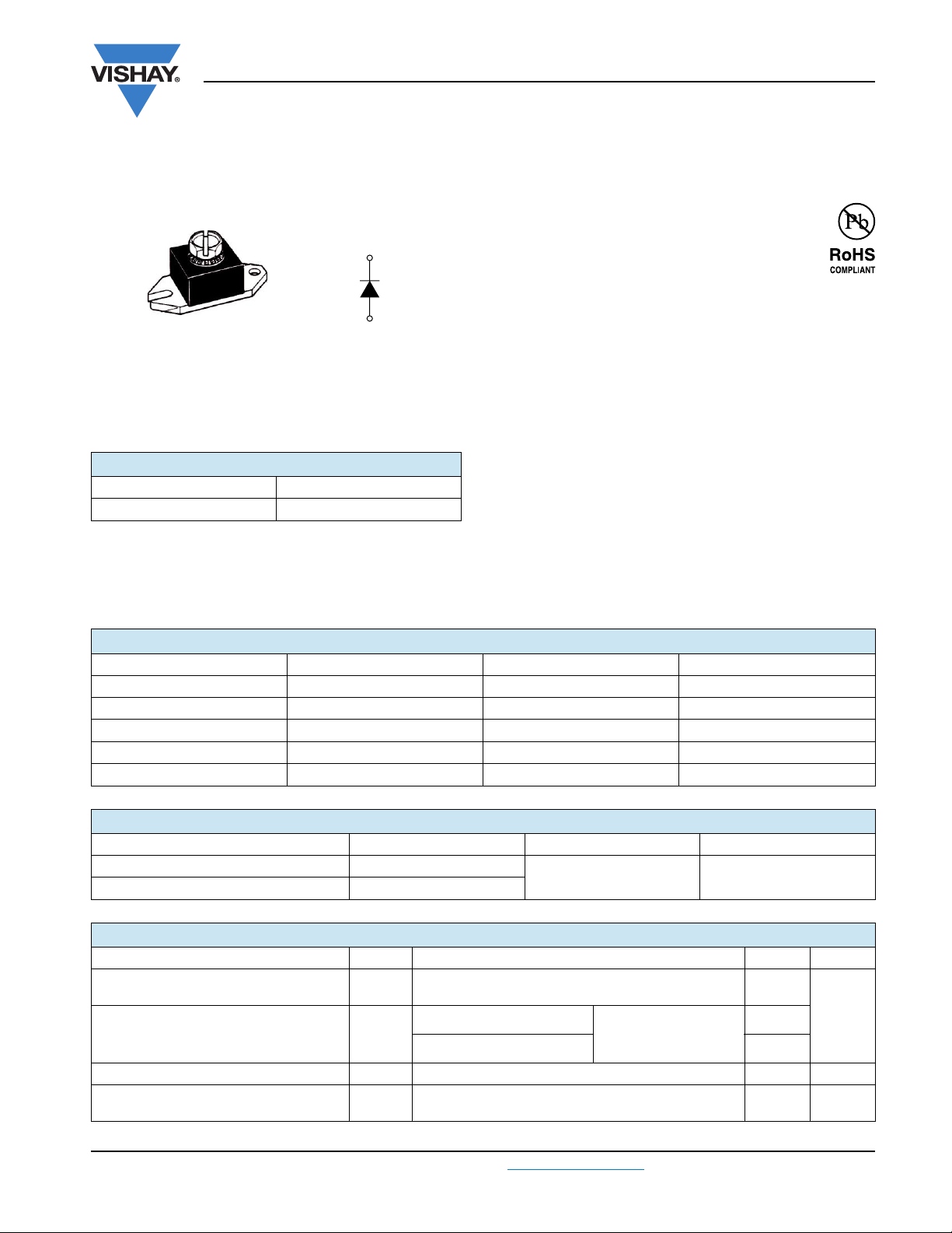
HALF-PAK (D-67) Reverse
PRODUCT SUMMARY
I
F(AV)
V
R
Schottky Rectifier, 240 A
FEATURES
Lug terminal cathode
Base anode
240 A
45 V
• 175 °C TJ operation
• Unique high power, HALF-PAK module
• Replaces four parallel DO-5’s
• Easier to mount and lower profile than DO-5’s
• High purity, high temperature epoxy encapsulation for
enhanced mechanical strength and moisture resistance
• Low forward voltage drop
• High frequency operation
• Guard ring for enhanced ruggedness and long term
reliability
• Compliant to RoHS directive 2002/95/EC
• Designed and qualified for industrial level
DESCRIPTION
The 241NQ045R high current Schottky rectifier module has
been optimized for low reverse leakage at high temperature.
The proprietary barrier technology allows for reliable
operation up to 175 °C junction temperature. Typical
applications are in switching power supplies, converters,
freewheeling diodes, and reverse battery protection.
241NQ045R
Vishay High Power Products
MAJOR RATINGS AND CHARACTERISTICS
SYMBOL CHARACTERISTICS VALUES UNITS
I
F(AV)
V
I
FSM
V
T
RRM
F
J
Rectangular waveform 240 A
Range 45 V
tp = 5 μs sine 25 000 A
240 Apk, TJ = 125 °C 0.59 V
Range - 55 to 175 °C
VOLTAGE RATINGS
PARAMETER SYMBOL 241NQ045R UNITS
Maximum DC reverse voltage V
Maximum working peak reverse voltage V
R
RWM
45 V
ABSOLUTE MAXIMUM RATINGS
PARAMETER SYMBOL TEST CONDITIONS VALUES UNITS
Maximum average forward current
See fig. 5
Maximum peak one cycle non-repetitive
surge current
See fig. 7
Non-repetitive avalanche energy E
Repetitive avalanche current I
I
F(AV)
I
FSM
AR
50 % duty cycle at TC = 130 °C, rectangular waveform 240
5 μs sine or 3 μs rect. pulse
10 ms sine or 6 ms rect. pulse 3450
TJ = 25 °C, IAS = 48 A, L = 0.28 mH 324 mJ
AS
Current decaying linearly to zero in 1 μs
Frequency limited by T
maximum VA = 1.5 x VR typical
J
Following any rated load
condition and with rated
V
applied
RRM
25 000
48 A
A
Document Number: 93111 For technical questions, contact: indmodules@vishay.com
Revision: 18-Nov-09 1
www.vishay.com
Page 4
241NQ045R
Vishay High Power Products
Schottky Rectifier, 240 A
ELECTRICAL SPECIFICATIONS
PARAMETER SYMBOL TEST CONDITIONS VALUES UNITS
240 A
Maximum forward voltage drop
See fig. 1
V
FM
480 A 0.82
(1)
240 A
480 A 0.72
Maximum reverse leakage current
See fig. 2
I
RM
Maximum junction capacitance C
Typical series inductance L
TJ = 25 °C
(1)
T
= 125 °C 180
J
VR = 5 VDC (test signal range 100 kHz to 1 MHz), 25 °C 10 300 pF
T
From top of terminal hole to mounting plane 5.0 nH
S
Maximum voltage rate of change dV/dt Rated V
T
= 25 °C
J
= 125 °C
T
J
V
= Rated V
R
R
R
0.69
0.59
20
mA
10 000 V/μs
Note
(1)
Pulse width < 300 μs, duty cycle < 2 %
THERMAL - MECHANICAL SPECIFICATIONS
PARAMETER SYMBOL TEST CONDITIONS VALUES UNITS
Maximum junction and
storage temperature range
Maximum thermal resistance,
junction to case
Typical thermal resistance,
case to heatsink
Approximate weight
Mounting torque
Terminal torque
minimum
maximum 58 (50)
minimum 58 (50)
maximum 86 (75)
Case style D-67 HALF-PAK Reverse
, T
T
J
Stg
R
R
thJC
thCS
DC operation
See fig. 4
Mounting surface, smooth and greased 0.15
- 55 to 175 °C
0.20
°C/W
25.6 g
0.9 oz.
40 (35)
Non-lubricated threads
kgf · cm
(lbf · in)
V
www.vishay.com For technical questions, contact: indmodules@vishay.com
Document Number: 93111
2 Revision: 18-Nov-09
Page 5
241NQ045R
Schottky Rectifier, 240 A
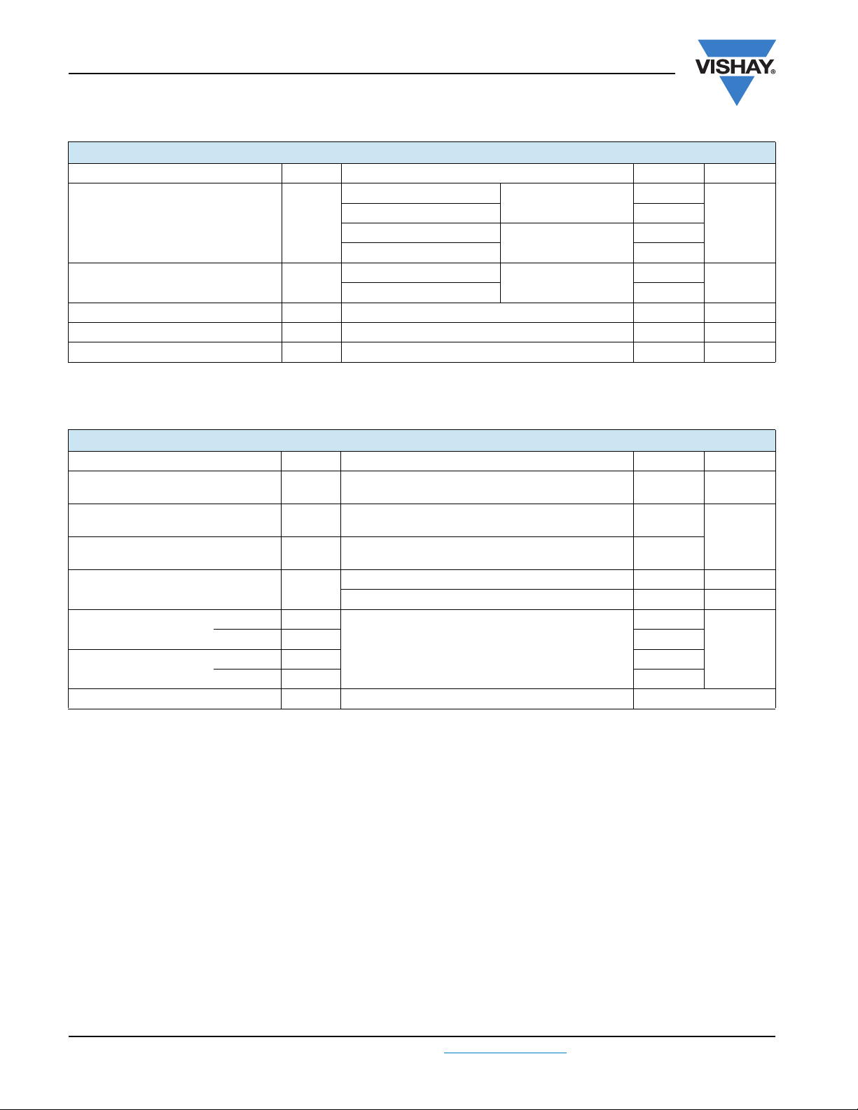
1000
100
F
T = 175° C
J
T = 125° C
J
T = 25°C
J
10
I nstan taneou s Forwar d Curr ent - I ( A)
Vishay High Power Products
10000
1000
R
Rev er se Current - I (mA)
Fig. 2 - Typical Values of Reverse Current vs.
10000
T
T = 175 °C
J
100
10
1
.1
.01
.001
150°C
125°C
100°C
75°C
50°C
25°C
0 5 10 15 20 25 30 35 40 45
Reverse Volt age - V (V)
R
Reverse Voltage
1
0.1.2.3.4.5.6.7.8.9
Forward Voltage Drop - V (V
)
FM
Fig. 1 - Maximum Forward Voltage Drop Characteristics
1
)
D = 0 .5 0
.1
thJC
pedance - Z (°C/W
Ther mal I m
D = 0 .3 3
D = 0 .2 5
D = 0 .1 7
D = 0 .0 8
.01
Single Pulse
.001
.0 0001 .00 01 .0 01 .0 1 .1 1 10 100
(Thermal Resi stance)
t , Rectangular Pulse Duration (Seconds)
1
Fig. 4 - Maximum Thermal Impedance Z
T = 25°C
J
Junction Capacitance - C (pF)
1000
0 1020304050
Reverse Volt age - V (V)
R
Fig. 3 - Typical Junction Capacitance vs. Reverse Voltage
P
DM
t
1
t
Not e s :
1. Duty factor D = t / t
2. Peak T = P x Z + T
thJC
2
1
JDM
Characteristics
2
thJC C
Document Number: 93111 For technical questions, contact: indmodules@vishay.com
www.vishay.com
Revision: 18-Nov-09 3
Page 6
241NQ045R
Vishay High Power Products
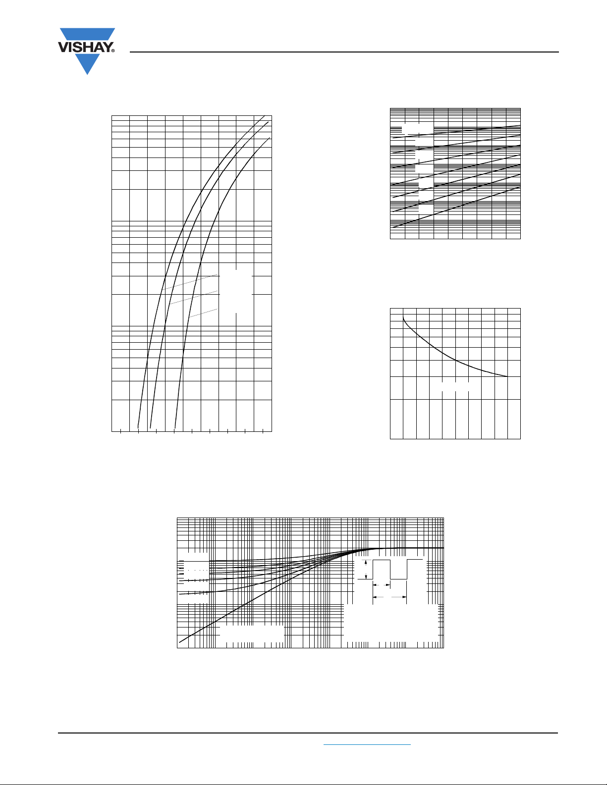
180
241NQ
170
160
150
140
130
Al l owabl e Case Temperature - (°C)
120
0 50 100 150 2 00 2 50 300 350
Average Forward Current - I (A)
Fig. 5 - Maximum Allowable Case Temperature vs.
Average Forward Current
R (DC) = 0.20°C/W
thJC
DC
F(AV)
100000
FSM
Schottky Rectifier, 240 A
Average Power Los s - ( Watt s)
Fig. 6 - Forward Power Loss Characteristics
At Any Rated Load Condition
And With Rated V Applied
Following Surge
RRM
220
D = 0. 0 8
200
D = 0. 1 7
180
D = 0. 2 5
D = 0. 3 3
160
D = 0. 5 0
140
120
RMS Li mit
100
80
60
40
20
0
0 50 100 150 200 2 50 30 0 350
Aver age For war d Current - I (A
DC
F(AV)
)
D.U.T.
Current
monitor
10000
Non-Repetitive Surge Current - I (A)
1000
10 100 1000 10000
Square Wave Pulse Duration - t (microsec)
p
Fig. 7 - Maximum Non-Repetitive Surge Current
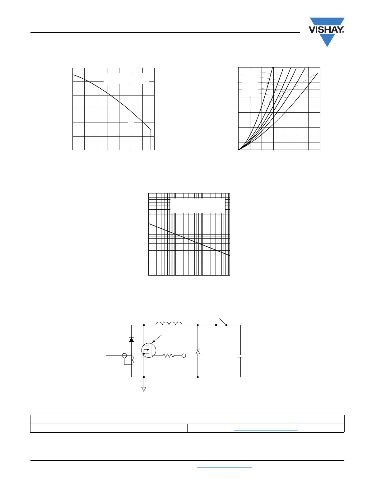
L
IRFP460
= 25 Ω
R
g
High-speed
switch
Freewheel
diode
40HFL40S02
Fig. 8 - Unclamped Inductive Test Circuit
V
= 25 V
d
+
LINKS TO RELATED DOCUMENTS
Dimensions www.vishay.com/doc?95378
www.vishay.com For technical questions, contact: indmodules@vishay.com
Document Number: 93111
4 Revision: 18-Nov-09
Page 7
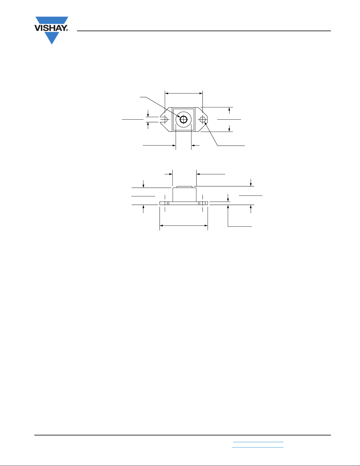
DIMENSIONS in millimeters (inches)
1/4-20 UNC-2B
Outline Dimensions
Vishay High Power Products
D-67 HALF-PAK Reverse
30.40 (1.197)
29.90 (1.177)
4.11 (0.162)
3.86 (0.152)
13.97 (0.550)
13.72 (0.540)
Ø 12.83 (0.505)
Ø 12.57 (0.495)
39.62 (1.560)
38.61 (1.520)
19.69 (0.775)
18.42 (0.725)
Ø 4.11 (0.162)
Ø 3.86 (0.152)
19.18 (0.755)
18.92 (0.745)
15.11 (0.595)
14.61 (0.575)
2.54 (0.100)
2.29 (0.090)
Document Number: 95378 For technical questions concerning discrete products, contact: diodestech@vishay.com
Revision: 12-Nov-09 For technical questions concerning module products, contact: indmodules@vishay.com
www.vishay.com
1
 Loading...