

Page 1

6121 Baker Road,
Suite 108
Minnetonka, MN 55345
www.chtechnology.com
Phone (952) 933-6190
Fax (952) 933-6223
1-800-274-4284
Thank you for downloading this document from C&H Technology, Inc.
Please contact the C&H Technology team for the following questions -
Technical
Application
Assembly
Availability
Pricing
Phone – 1-800-274-4284
E-Mail – sales@chtechnology.com
www.chtechnology.com - SPECIALISTS IN POWER ELECTRONIC COMPONENTS AND ASSEMBLIES - www.chtechnology.com
Page 2
20MT120UF
Document Number: 93588
www.vishay.com
1
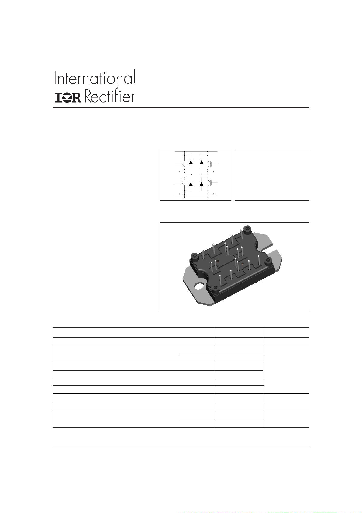
"FULL-BRIDGE" IGBT MTP
Features
• UltraFast Non Punch Through (NPT)
Technology
• Positive V
• 10µs Short Circuit Capability
• HEXFRED
UltraSoft Reverse Recovery
• Low Diode V
• Square RBSOA
• Aluminum Nitride DBC
• Very Low Stray Inductance Design for
High Speed Operation
• UL approved (File E78996)
Benefits
• Optimized for Welding, UPS and SMPS
Applications
• Rugged with UltraFast Performance
• Benchmark Efficiency above 20KHz
• Outstanding ZVS and Hard Switching
Operation
• Low EMI, requires Less Snubbing
• Excellent Current Sharing in Parallel
Operation
• Direct Mounting to Heatsink
• PCB Solderable Terminals
• Very Low Junction-to-Case Thermal
Resistance
Temperature Coefficient
CE(ON)
TM
Antiparallel Diodes with
F
UltraFast NPT IGBT
V
= 1200V
CES
I
= 40A
C
T
= 25°C
C
MMTP5/I27124 rev. D 02/03
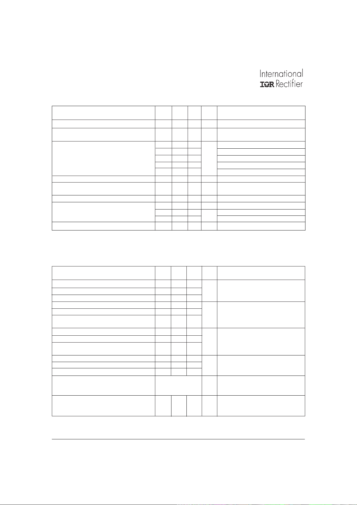
Absolute Maximum Ratings
Parameters Max Units
V
I
I
I
I
I
V
V
P
CES
C
CM
LM
F
FM
GE
ISOL
D
Collector-to-Emitter Breakdown Voltage 1200 V
Continuos Collector Current @ TC = 25°C 40 A
Pulsed Collector Current 100
Clamped Inductive Load Current 100
Diode Continuous Forward Current @ TC = 106°C 25
Diode Maximum Forward Current 100
Gate-to-Emitter Voltage ± 20 V
RMS Isolation Voltage, Any Terminal to Case, t = 1 min 2500
Maximum Power Dissipation (only IGBT) @ TC = 25°C 240 W
@ TC = 106°C 20
@ TC = 100°C 96
Page 3
20MT120UF
Document Number: 93588
www.vishay.com
2
I27124 rev. D 02/03
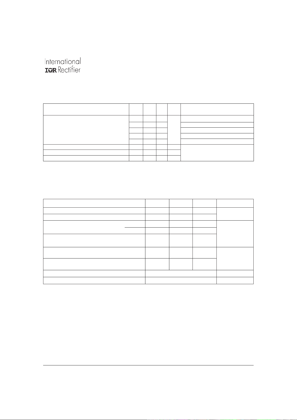
Electrical Characteristics @ T
Parameters Min Typ Max Units Test Conditions
V
(BR)CES
∆V
∆T
V
V
∆V
∆T
g
fe
I
CES
I
GES
(1) I
CE(ON)
GE(th)
Collector-to-Emitter Breakdown Voltage 1200 V VGE = 0V, IC = 250µA
/ Temperature Coeff. of +1.3 V/°C VGE = 0V, IC = 3mA (25-125°C)
(BR)CES
Breakdown Voltage
J
Collector-to-Emitter Saturation Voltage 3.29 3.59 V VGE = 15V, IC = 20A
Gate Threshold Voltage 4 6 V VCE = VGE, IC = 250µA
/ Temperature Coeff. of -14 mV/°C VCE = VGE, IC = 3mA (25-125°C)
GE(th)
Threshold Voltage
J
Transconductance 17.5 S VCE = 50V, IC = 20A, PW = 80µs
Zero Gate Voltage Collector Current
Gate-to-Emitter Leakage Current ±250 nA VGE = ± 20V
includes also opposite leg overall leakage
CES
Switching Characteristics @ T
Parameters Min Typ Max Units Test Conditions
= 25°C (unless otherwise specified)
J
4.42 4.66 VGE = 15V, IC = 40A
3.87 4.11 VGE = 15V, IC = 20A TJ = 125°C
5.32 5.70 VGE = 15V, IC = 40A TJ = 125°C
3.99 4.27 VGE = 15V, IC = 20A TJ = 150°C
(1)
250 µA VGE = 0V, VCE = 1200V, TJ = 25°C
0.7 3.0 mA VGE = 0V, VCE = 1200V, TJ = 125°C
2.9 9.0 VGE = 0V, VCE = 1200V, TJ = 150°C
= 25°C (unless otherwise specified)
J
Q
g
Q
ge
Q
gc
E
on
E
off
E
tot
Total Gate Charge (turn-on) 176 264 nC IC = 20A
Gate-Emitter Charge (turn-on) 19 30 VCC = 600V
Gate-Collector Charge (turn-on) 89 134 VGE = 15V
Turn-On Switching Loss 513 770 µJ VCC = 600V, IC = 20A
Turn-Off Switching Loss 402 603 VGE = 15V, Rg = 5Ω, L = 200µH
Total Switching Loss 915 1373 TJ = 25°C, Energy losses include tail
and diode reverse recovery
E
on
E
off
E
tot
Turn-On Switching Loss 930 1395 µJ VCC = 600V, IC = 20A
Turn-Off Switching Loss 610 915 VGE = 15V, Rg = 5Ω, L = 200µH
Total Switching Loss 1540 2310 TJ = 125°C, Energy losses include tail
and diode reverse recovery
C
ies
C
oes
C
res
Input Capacitance 2530 3790 pF VGE = 0V
Output Capacitance 344 516 VCC = 30V
Reverse Transfer Capacitance 78 117 f = 1.0 MHz
RBSOA Reverse Bias Safe Operating Area full square TJ = 150°C, IC = 120A
VCC = 1000V, Vp = 1200V
Rg = 5Ω, VGE = +15V to 0V
SCSOA Short Circuit Safe Operating Area 10 µs TJ = 150°C
VCC = 900V, Vp = 1200V
Rg = 5Ω, VGE = +15V to 0V
Page 4
20MT120UF
Document Number: 93588
www.vishay.com
3
I27124 rev. D 02/03
Diode Characteristics @ T
= 25°C (unless otherwise specified)
J
Parameters Min Typ Max Units Test Conditions
V
FM
E
rec
trr Diode Reverse Recovery Time 98 150 ns VCC = 600V, IC = 20A
Irr Peak Reverse Recovery Current 33 50 A TJ = 125°C
Diode Forward Voltage Drop 2.48 2.94 V IC = 20A
3.28 3.90 IC = 40A
2.44 2.84 IC = 20A, TJ = 125°C
3.45 4.14 IC = 40A, TJ = 125°C
2.21 2.93 IC = 20A, TJ = 150°C
Reverse Recovery Energy of the Diode 420 630 µJ VGE = 15V, Rg = 5Ω, L = 200µH
Thermal- Mechanical Specifications
Parameters Min Typ Max Units
T
J
T
STG
R
thJC
R
thCS
T Mounting Torque (2) 3 ± 10% Nm
Wt Weight 66 g (oz)
Operating Junction Temperature Range - 40 150 °C
Storage Temperature Range - 40 125
Junction-to-Case IGBT 0.35 0.52 °C/ W
Diode 0.40 0.61
Case-to-Sink Module 0.06
(Heatsink Compound Thermal Conductivity = 1 W/mK)
Clearance (external shortest distance in air 5.5 mm
between two terminals)
Creepage (shortest distance along external 8
surface of the insulating material between 2 terminals)
(2) A mounting compound is recommended and the torque should be checked after 3 hours to allow for the spread of the
compound. Lubricated threads
Page 5
20MT120UF
Document Number: 93588
www.vishay.com
4
I27124 rev. D 02/03
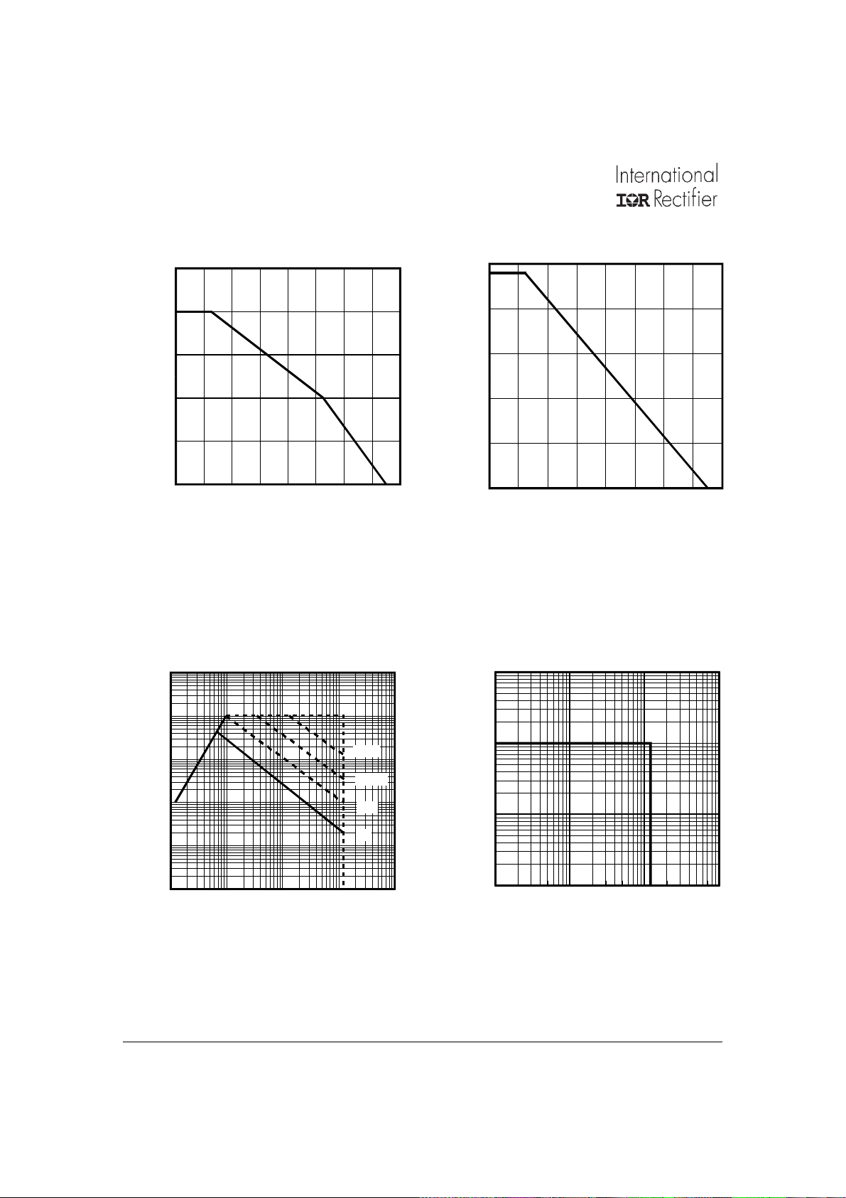
(A)
C
I
1000
50
40
30
20
10
0
0 20 40 60 80 100 120 140 160
TC (°C)
Fig. 1 - Maximum DC Collector Current vs.
Case Temperature
(W)
tot
P
250
200
150
100
50
0
0 20 40 60 80 100 120 140 160
TC (°C)
Fig. 2 - Power Dissipation vs. Case
Temperature
1000
100
10
(A)
C
I
1
0.1
0.01
1 10 100 1000 10000
V
(V)
CE
Fig. 3 - Forward SOA
TC = 25°C; T
≤ 150°C
J
10 µs
100 µs
1ms
DC
100
(A)
C
I
10
1
10 100 1000 10000
V
(V)
CE
Fig. 4 - Reverse Bias SOA
TJ = 150°C; V
GE
=15V
Page 6

20MT120UF
Document Number: 93588
www.vishay.com
5
I27124 rev. D 02/03
100
VGE = 18V
VGE = 15V
VGE = 12V
80
VGE = 10V
VGE = 8.0V
60
(A)
CE
I
40
20
0
0246810
V
(V)
CE
Fig. 5 - Typ. IGBT Output Characteristics
TJ = -40°C; tp = 80µs
100
VGE = 18V
VGE = 15V
VGE = 12V
80
VGE = 10V
VGE = 8.0V
60
(A)
CE
I
40
100
VGE = 18V
VGE = 15V
VGE = 12V
80
VGE = 10V
VGE = 8.0V
60
(A)
CE
I
40
20
0
0246810
V
(V )
CE
Fig. 6 - Typ. IGBT Output Characteristics
TJ = 25°C; tp = 80µs
120
-40°C
25°C
125°C
(A)
I
100
F
80
60
40
20
0
0246810
V
(V)
CE
Fig. 7 - Typ. IGBT Output Characteristics
TJ = 125°C; tp = 80µs
20
0
0.01.02.03.04.05.0
VF (V)
Fig. 8 - Typ. Diode Forward Characteristics
tp = 80µs
Page 7

20MT120UF
Document Number: 93588
www.vishay.com
6
I27124 rev. D 02/03
20
18
16
14
ICE = 40A
I
= 20A
CE
I
= 10A
CE
12
(V)
10
CE
V
8
6
4
2
0
5101520
V
(V)
GE
Fig. 9 - Typical V
TJ = -40°C
CE
vs. V
GE
20
18
16
14
ICE = 10A
I
= 20A
CE
I
= 40A
CE
12
(V)
10
CE
V
8
6
4
2
0
5101520
V
(V)
GE
(A)
I
20
18
16
14
ICE = 10A
I
= 20A
CE
I
= 40A
CE
12
(V)
10
CE
V
8
6
4
2
0
5101520
V
(V)
GE
Fig. 10 - Typical V
CE
vs. V
GE
TJ = 25°C
300
250
TJ = 25°C
TJ = 150°C
200
150
CE
100
50
0
0 5 10 15 20
V
(V)
GE
Fig. 11 - Typical V
TJ = 125°C
CE
vs. V
GE
Fig. 12 - Typ. Transfer Characteristics
VCE = 50V; tp = 10µs
Page 8

20MT120UF
Document Number: 93588
www.vishay.com
7
I27124 rev. D 02/03
(µJ)
Energy
2400
2000
E
1600
ON
1200
E
800
OFF
400
0
0 1020304050
IC (A )
Fig. 13 - Typ. Energy Loss vs. I
TJ = 150°C; L=1.4mH; VCE= 400V
C
RG= 5Ω; VGE= 15V
2000
1000
td
OFF
t
100
Swiching Time (ns)
10
F
td
ON
t
R
0 10 20 30 40 50
IC (A)
Fig. 14 - Typ. Switching Time vs. I
TJ = 150°C; L=1.4mH; VCE= 400V
RG= 100Ω; VGE= 15V
1000
C
1600
1200
E
ON
E
800
Energy (µJ)
400
0
0 10 20 30 40 50 60
RG ()
Fig. 15 - Typ. Energy Loss vs. R
TJ = 150°C; L=1.4mH; VCE= 400V
ICE= 5.0A; VGE= 15V
OFF
td
OFF
t
100
F
td
ON
Swiching Time (ns)
t
R
10
0 10 20 30 40 50 60
RG ()
G
Fig. 16 - Typ. Switching Time vs. R
TJ = 150°C; L=1.4mH; VCE= 400V
G
ICE= 5.0A; VGE= 15V
Page 9

20MT120UF
Document Number: 93588
www.vishay.com
8
I27124 rev. D 02/03
40
30
(A)
20
RR
I
10
0
0 5 10 15 20 25 30 35
IF (A)
Fig. 17 - Typical Diode I
TJ = 150°C
40
RR
vs. I
40
R
5.0
Ω
G =
R
10
Ω
G =
R
30
Ω
G =
R
50
Ω
G =
F
30
(A)
20
RR
I
10
0
0 10 20 30 40 50 60
RG (
Ω)
Fig. 18 - Typical Diode I
TJ = 150°C; IF = 5.0A
RR
vs. R
G
3.0
35
30
(A)
25
RR
I
20
15
10
0 200 400 600 800 1000
diF /dt (A/µs)
Fig. 19- Typical Diode I
VCC= 400V; VGE= 15V;
vs. diF/dt
RR
ICE= 5.0A; TJ = 150°C
2.5
10
Ω
2.0
30
(µC)
1.5
RR
Q
1.0
50
Ω
Ω
10A
0.5
0.0
0 200 400 600 800 1000 1200
diF /dt (A/µs)
Fig. 20 - Typical Diode Q
VCC= 400V; VGE= 15V;TJ = 150°C
RR
5.0
Ω
30A
20A
Page 10

10000
Document Number: 93588
www.vishay.com
9
Cies
1000
Coes
100
Capacitance (pF)
10
0 20 40 60 80 100
V
(V )
CE
20MT120UF
I27124 rev. D 02/03
Cres
Fig. 21- Typ. Capacitance vs. V
VGE= 0V; f = 1MHz
16
14
12
10
(V)
8
GE
V
6
4
2
0
0 40 80 120 160 200
Q G, Total Gate Charge (nC)
Fig. 22 - Typical Gate Charge vs. V
I
= 5.0A; L = 600µH
CE
CE
600V
GE
Page 11

20MT120UF
τ
τ
Document Number: 93588
www.vishay.com
10
I27124 rev. D 02/03
1
D = 0.50
)
0.1
thJC
0.01
0.001
Thermal Response ( Z
0. 0001
0.20
0.10
0.05
R
R
0.02
0.01
SINGLE PULSE
( THERMAL RESPONSE )
τ
J
τ
J
τ
1
τ
1
Ci= τi/Ri
1
R
1
R
2
3
R
2
τ
2
τ
2
Ri (°C/W) τi (sec)
R
3
τ
C
0.161 0.000759
τ
3
0.210 0.017991
τ
3
0.147 0.06094
Notes:
1. Duty Factor D = t1/t2
2. Peak Tj = P dm x Zthjc + Tc
1E-006 1E-005 0. 0001 0.001 0.01 0. 1 1 10
t1 , Rectangular Pulse Duration (sec)
Fig 23. Maximum Transient Thermal Impedance, Junction-to-Case (IGBT)
1
D = 0.50
)
0.1
thJC
0.20
0.10
0.05
R
R
R
2
3
R
2
τ
2
τ
2
Ri (°C/W) τi (sec)
R
3
τ
C
0.238 0.001017
τ
3
0.312 0.033081
τ
3
0.061 0.77744
Notes:
1. Duty Factor D = t1/t2
2. Peak Tj = P dm x Zthjc + Tc
Thermal Response ( Z
0.01
0.001
0.02
0.01
SINGLE PULSE
( THERMAL RESPONSE )
τ
J
τ
J
τ
1
τ
1
Ci= τi/Ri
1
R
1
0.0001
1E-006 1E-005 0. 0001 0.001 0.01 0.1 1 10
t1 , Rectangul ar Pulse Duration (sec )
Fig 24. Maximum Transient Thermal Impedance, Junction-to-Case (DIODE)
Page 12

20MT120UF
Document Number: 93588
www.vishay.com
11
I27124 rev. D 02/03
L
0
1K
Fig. CT.1 - Gate Charge Circuit (turn-off)
Driver
DUT
L
VCC
80 V
DUT
1000V
Rg
Fig. CT.2 - RBSOA Circuit
diode clamp /
DUT
L
D
C
DUT
Fig. CT.3 - S.C. SOA Circuit
900V
- 5V
DUT /
DRIVER
Rg
Fig. CT.4 - Switching Loss Circuit
VCC
Page 13

20MT120UF
Document Number: 93588
www.vishay.com
12
I27124 rev. D 02/03
Outline Table
Electrical Diagram
Resistance in ohms
Dimensions in millimetres
Page 14

Ordering Information Table
Document Number: 93588
www.vishay.com
13
Device Code
20MT120UF
I27124 rev. D 02/03
20 MT 120 U F
1 2 3
1- Current rating (20 = 20A)2- Essential Part Number3- Voltage code (120= 1200V)4- Speed/ Type (U = Ultra Fast IGBT)5- Circuit Configuration (F = Full Bridge)6- Special Option
4
5
This product has been designed and qualified for Industrial Level.
Data and specifications subject to change without notice.
Qualification Standards can be found on IR's Web site.
IR WORLD HEADQUARTERS: 233 Kansas St., El Segundo, California 90245, USA Tel: (310) 252-7105
TAC Fax: (310) 252-7309
01/03
Page 15

Legal Disclaimer Notice
Vishay
Notice
The products described herein were acquired by Vishay Intertechnology, Inc., as part of its acquisition of
International Rectifier’s Power Control Systems (PCS) business, which closed in April 2007. Specifications of the
products displayed herein are pending review by Vishay and are subject to the terms and conditions shown below.
Specifications of the products displayed herein are subject to change without notice. Vishay Intertechnology, Inc., or
anyone on its behalf, assumes no responsibility or liability for any errors or inaccuracies.
Information contained herein is intended to provide a product description only. No license, express or implied, by
estoppel or otherwise, to any intellectual property rights is granted by this document. Except as provided in Vishay's
terms and conditions of sale for such products, Vishay assumes no liability whatsoever, and disclaims any express
or implied warranty, relating to sale and/or use of Vishay products including liability or warranties relating to fitness
for a particular purpose, merchantability, or infringement of any patent, copyright, or other intellectual property right.
The products shown herein are not designed for use in medical, life-saving, or life-sustaining applications.
Customers using or selling these products for use in such applications do so at their own risk and agree to fully
indemnify Vishay for any damages resulting from such improper use or sale.
International Rectifier
are registered trademarks of International Rectifier Corporation in the U.S. and other countries. All other product
names noted herein may be trademarks of their respective owners.
®
, IR®, the IR logo, HEXFET®, HEXSense®, HEXDIP®, DOL®, INTERO®, and POWIRTRAIN
®
Document Number: 99901 www.vishay.com
Revision: 12-Mar-07 1
 Loading...