

Page 1

6121 Baker Road,
Suite 108
Minnetonka, MN 55345
www.chtechnology.com
Phone (952) 933-6190
Fax (952) 933-6223
1-800-274-4284
Thank you for downloading this document from C&H Technology, Inc.
Please contact the C&H Technology team for the following questions -
Technical
Application
Assembly
Availability
Pricing
Phone – 1-800-274-4284
E-Mail – sales@chtechnology.com
www.chtechnology.com - SPECIALISTS IN POWER ELECTRONIC COMPONENTS AND ASSEMBLIES - www.chtechnology.com
Page 2
MTK
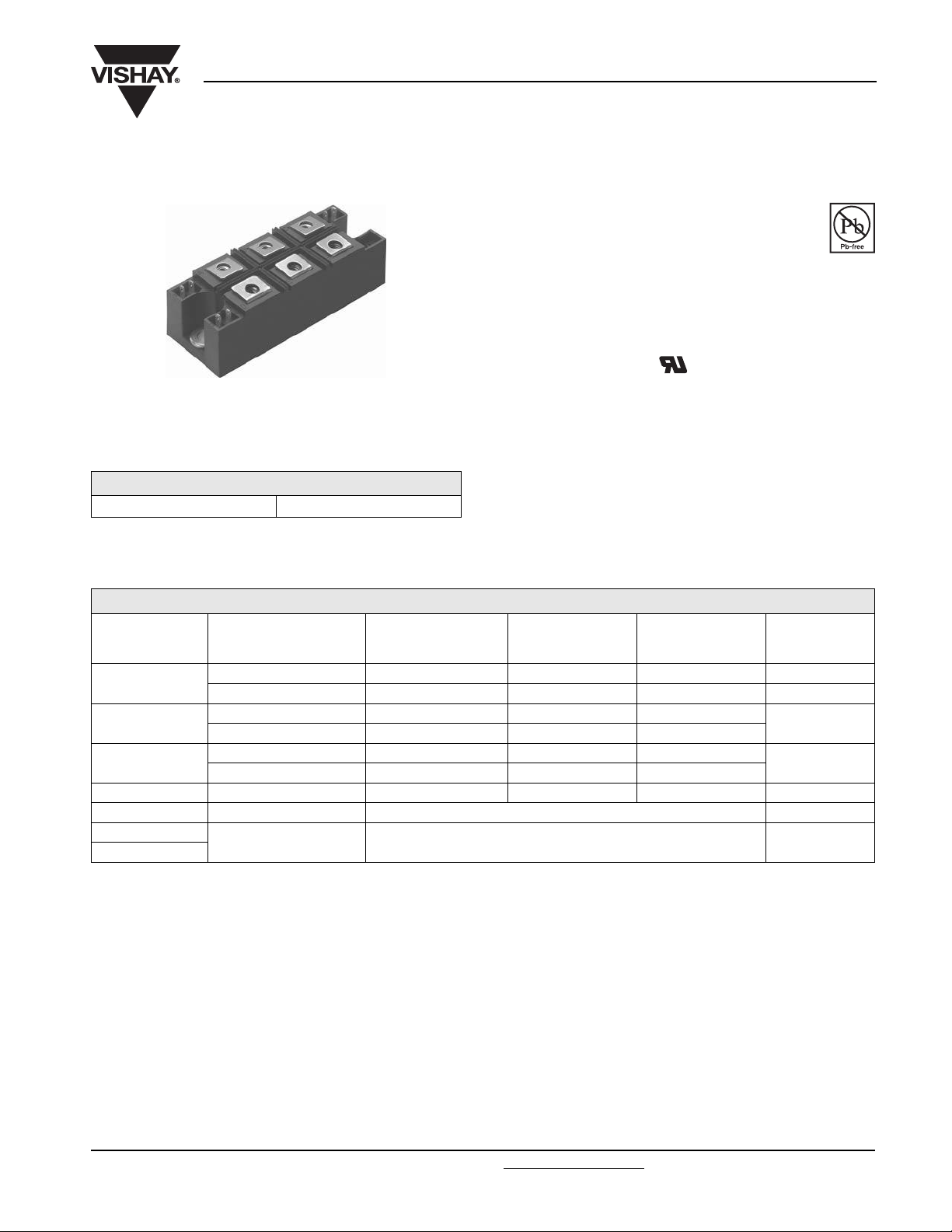
PRODUCT SUMMARY
I
O
53-93-113MT..KPbF Series
Vishay High Power Products
Three Phase Controlled Bridge
(Power Modules), 55 A to 110 A
FEATURES
• Package fully compatible with the industry
standard INT-A-PAK power modules series
• High thermal conductivity package, electrically
insulated case
• Excellent power volume ratio
55 A to 110 A
• 4000 V
• UL E78996 approved
• Totally lead (Pb)-free
• Designed and qualified for industrial level
DESCRIPTION
A range of extremely compact, encapsulated three phase
controlled bridge rectifiers offering efficient and reliable
operation. They are intended for use in general purpose and
heavy duty applications.
isolating voltage
RMS
RoHS
COMPLIANT
MAJOR RATINGS AND CHARACTERISTICS
53MT.K
SYMBOL CHARACTERISTICS
I
O
I
FSM
2
t
I
2
√t 7700 45 250 63 800 A2√s
I
V
RRM
T
Stg
T
J
T
C
50 Hz 390 950 1130
60 Hz 410 1000 1180
50 Hz 770 4525 6380
60 Hz 700 4130 5830
Range 800 to 1600 V
Range - 40 to 125 °C
52MT.K
51MT.K
55 90 110 A
85 85 85 °C
93MT.K
92MT.K
91MT.K
113MT.K
112MT.K
111MT.K
UNITS
A
A2s
Document Number: 94353 For technical questions, contact: ind-modules@vishay.com
Revision: 29-Apr-08 1
www.vishay.com
Page 3
53-93-113MT..KPbF Series
Vishay High Power Products
Three Phase Controlled Bridge
(Power Modules), 55 A to 110 A
ELECTRICAL SPECIFICATIONS
VOLTAGE RATINGS
V
, MAXIMUM
RRM
TYPE NUMBER
VOLTAGE
CODE
REPETITIVE PEAK
REVERSE VOLTAGE
V
80 800 900 800
100 1000 1100 1000
53/52/51MT..K
120 1200 1300 1200
140 1400 1500 1400
160 1600 1700 1600
80 800 900 800
100 1000 1100 1000
93/92/91MT..K
113/112/111MT..K
120 1200 1300 1200
140 1400 1500 1400
160 1600 1700 1600
FORWARD CONDUCTION
PARAMETER SYMBOL TEST CONDITIONS
Maximum DC output current
at case temperature
I
Maximum peak, one-cycle
forward, non-repetitive
I
TSM
on state surge current
2
Maximum I
Maximum I
Low level value of
threshold voltage
High level value of
threshold voltage
Low level value on-state
slope resistance
High level value on-state
slope resistance
Maximum on-state
voltage drop
t for fusing I2t
2
√t for fusing I2√t t = 0.1 to 10 ms, no voltage reapplied 7700 45 250 63 800 A2√s
V
T(TO)1
V
T(TO)2
r
r
V
Maximum non-repetitve
rate of rise of turned on
dI/dt
current
Maximum holding current I
Maximum latching current I
www.vishay.com For technical questions, contact: ind-modules@vishay.com
2 Revision: 29-Apr-08
120° rect. conduction angle
O
t = 10 ms
t = 8.3 ms 410 1000 1180
t = 10 ms
t = 8.3 ms 345 840 1000
t = 10 ms
t = 8.3 ms 700 4130 5830
t = 10 ms
t = 8.3 ms 500 2920 4120
(16.7 % x π x I
(I > π x I
(16.7 % x π x I
t1
(I > π x I
t2
Ipk = 150 A, TJ = 25 °C, tp = 400 µs single junction 2.68 1.65 1.57 V
TM
T
= 25 °C, from 0.67 V
J
I
= 500 mA, tr < 0.5 µs, tp > 6 µs
g
TJ = 25 °C, anode supply = 6 V,
H
resistive load, grate open circuit
TJ = 25 °C, anode supply = 6 V, resistive load 400
L
No voltage
reapplied
100 % V
reapplied
No voltage
reapplied
100 % V
reapplied
T(AV)
), TJ maximum 1.45 1.27 1.27
T(AV)
T(AV)
), TJ maximum 11.04 3.59 3.37
T(AV)
V
, MAXIMUM
RSM
NON-REPETITIVE PEAK
REVERSE VOLTAGE
V
RRM
Initial T
= TJ maximum
J
RRM
< I < π x I
< I < π x I
DRM
), TJ maximum 1.17 1.09 1.04
T(AV)
), TJ maximum 12.40 4.10 3.93
T(AV)
, ITM = π x I
T(AV)
V
, MAXIMUM REPETITIVE
DRM
PEAK OFF-STATE VOLTAGE,
GATE OPEN CIRCUIT
V
53MT.K
52MT.K
51MT.K
55 90 110 A
85 85 85 °C
390 950 1130
330 800 950
770 4525 6380
540 3200 4510
,
I
RRM/IDRM
MAXIMUM
AT T
= 125 °C
J
mA
10
20
93MT.K
92MT.K
91MT.K
113MT.K
112MT.K
111MT.K
150 A/µs
200
Document Number: 94353
,
UNITS
A
A2s
V
mΩ
mA
Page 4

53-93-113MT..KPbF Series
Three Phase Controlled Bridge
(Power Modules), 55 A to 110 A
BLOCKING
PARAMETER SYMBOL TEST CONDITIONS
RMS isolation voltage V
Maximum critical rate of rise
of off-state voltage
ISOL
dV/dt
Note
(1)
Available with dV/dt = 1000 V/µs, to complete code add S90 i. e. 113MT160KBS90
TRIGGERING
PARAMETER SYMBOL TEST CONDITIONS
Maximum peak gate power P
Maximum average gate power P
Maximum peak gate current I
Maximum peak negative
gate voltage
Maximum required DC gate
voltage to trigger
Maximum required DC gate
current to trigger
Maximum gate voltage
that will not trigger
Maximum gate current
that will not trigger
TJ = 25 °C all terminal shorted, f = 50 Hz, t = 1 s 4000 V
TJ = TJ maximum, linear to 0.67 V
(1)
gate open circuit
GM
G(AV)
GM
- V
TJ = TJ maximum
GT
TJ = - 40 °C
T
V
GT
I
GT
V
GD
I
GD
= 25 °C 2.5
J
= 125 °C 1.7
T
J
TJ = - 40 °C 270
= 25 °C 150
J
T
= 125 °C 80
J
TJ = TJ maximum, rated V
Anode supply = 6 V,
resistive load
DRM
,
DRM
applied
Vishay High Power Products
53MT.K
52MT.K
51MT.K
53MT.K
52MT.K
51MT.K
93MT.K
92MT.K
91MT.K
500 V/µs
93MT.K
92MT.K
91MT.K
0.25 V
113MT.K
112MT.K
UNITS
111MT.K
113MT.K
112MT.K
UNITS
111MT.K
10
2.5
W
2.5 A
10
4.0
V
mAT
6mA
THERMAL AND MECHANICAL SPECIFICATIONS
93MT.K
92MT.K
91MT.K
- 40 to 125 °C
PARAMETER SYMBOL TEST CONDITIONS
Maximum junction operating
and storage temperature range
T
, T
J
Stg
53MT.K
52MT.K
51MT.K
DC operation per module 0.18 0.14 0.12
Maximum thermal resistance,
junction to case
R
thJC
DC operation per junction 1.07 0.86 0.70
120 °C rect. conduction angle per module 0.19 0.15 0.12
120 °C rect. conduction angle per junction 1.17 0.91 0.74
Maximum thermal resistance,
case to heatsink per module
Mounting
torque ± 10 %
to heatsink
to terminal 3 to 4
R
thCS
Approximate weight 225 g
Mounting surface smooth, flat and grased 0.03
A mounting compound is recommended and
4 to 6
the torque should be rechecked after a period
of 3 hours to allow for the spread of the
compound. Lubricated threads.
Document Number: 94353 For technical questions, contact: ind-modules@vishay.com
Revision: 29-Apr-08 3
113MT.K
112MT.K
111MT.K
UNITS
K/W
Nm
www.vishay.com
Page 5

53-93-113MT..KPbF Series
Vishay High Power Products
Three Phase Controlled Bridge
(Power Modules), 55 A to 110 A
ΔR CONDUCTION PER JUNCTION
SINUSOIDAL CONDUCTION
MAXIMUM
AT T
DEVICES
J
180° 120° 90° 60° 30° 180° 120° 90° 60° 30°
53/52/51MT.K 0.072 0.085 0.108 0.152 0.233 0.055 0.091 0.117 0.157 0.236
113/112/111MT.K 0.027 0.033 0.042 0.057 0.081 0.023 0.037 0.046 0.059 0.082
Note
• Table shows the increment of thermal resistance R
130
120
110
53MT..K Series
120°
(Rect)
when devices operate at different conduction angles than DC
thJC
RECTANGULAR CONDUCTION
AT TJ MAXIMUM
1000
TJ = 25 °C
100
TJ = 125 °C
UNITS
K/W93/92/91MT.K 0.033 0.039 0.051 0.069 0.099 0.027 0.044 0.055 0.071 0.100
100
Maximum Allowable
Case Temperature (°C)
~
90
80
10 20 304050
0
Total Output Current (A)
Fig. 1 - Current Ratings Characteristic Fig. 2 - Forward Voltage Drop Characteristics
220
53MT..K Series
200
T
= 125 °C
180
160
140
120
100
Maximum Total Power Loss (W)
J
80
60
40
20
0
51510 25 353020 40 5045
0
Total Output Current (A)
+
-
120°
(Rect)
10
Instantaneous On-State Current (A)
1
220
200
180
160
140
120
100
0
80
60
40
20
0
0
60
Maximum Total Power Loss (W)
55
Fig. 3 - Total Power Loss Characteristics
53MT..K Series
Per junction
21 3 456
Instantaneous On-State Voltage (V)
R
0.3 K/W
0.4 K/W
0.5 K/W
0.7 K/W
1.0 K/W
1.5 K/W
25 50 75 100
0.12 K/W
0.2 K/W
thSA
= 0.05 K/W - ΔR
Maximum Allowable Ambient
Temperature (°C)
7
125
www.vishay.com For technical questions, contact: ind-modules@vishay.com
Document Number: 94353
4 Revision: 29-Apr-08
Page 6

53-93-113MT..KPbF Series
(Power Modules), 55 A to 110 A
350
300
250
200
On-State Current (A)
Peak Half Sine Wave
53MT..K Series
150
1
Fig. 4 - Maximum Non-Repetitive Surge Current
400
350
300
At any rated load condition and with
rated V
Per junction
applied following surge.
RRM
Initial T
at 60 Hz 0.0083 s
at 50 Hz 0.0100 s
Number of Equal Amplitude
Half Cycle Current Pulses (N)
Maximum non-repetitive surge current
versus pulse train duration. Control
of conduction may not be maintained.
Initial TJ = 125 °C
No voltage reapplied
Rated V
Three Phase Controlled Bridge
130
= 125 °C
J
RRM
10
reapplied
100
120
110
100
Maximum Allowable
90
Case Temperature (°C)
80
1000
100
Vishay High Power Products
93MT..K Series
120°
(Rect)
~
20 40 60 80 1000
Total Output Current (A)
Fig. 6 - Current Ratings Characteristic
+
-
250
On-State Current (A)
Peak Half Sine Wave
200
53MT..K Series
Per junction
150
0.1 10.01
Pulse Train Duration (s)
Fig. 5 - Maximum Non-Repetitive Surge Current
300
93MT..K Series
T
250
200
150
100
50
= 125 °C
J
120°
(Rect)
Maximum Total Power Loss (W)
0
10 20 304050 7060
0
Total Output Current (A)
10
Instantaneous On-State Current (A)
300
250
200
150
100
50
Maximum Total Power Loss (W)
9080
Fig. 8 - Total Power Loss Characteristics
TJ = 25 °C
TJ = 125 °C
93MT..K Series
Per junction
1
1.0 2.01.50.5 2.5 3.0 3.5
Total Output Current
Fig. 7 - Forward Voltage Drop Characteristics
0.12 K/W
0.2 K/W
0.3 K/W
0.4 K/W
0.5 K/W
0.7 K/W
1.0 K/W
1.5 K/W
0
25 50 75 100
0
R
thSA
= 0.05 K/W - ΔR
Maximum Allowable Ambient
Temperature (°C)
4.0
125
Document Number: 94353 For technical questions, contact: ind-modules@vishay.com
www.vishay.com
Revision: 29-Apr-08 5
Page 7

53-93-113MT..KPbF Series
Vishay High Power Products
850
800
750
700
650
600
550
On-State Current (A)
Peak Half Sine Wave
500
93MT..K Series
450
Per junction
400
1
Fig. 9 - Maximum Non-Repetitive Surge Current
1000
900
800
700
600
500
On-State Current (A)
Peak Half Sine Wave
400
93MT..K Series
300
0.01
Fig. 10 - Maximum Non-Repetitive Surge Current
At any rated load condition and with
rated V
applied following surge.
RRM
Initial TJ = 125 °C
at 60 Hz 0.0083 s
at 50 Hz 0.0100 s
10
Number of Equal Amplitude
Half Cycle Current Pulses (N)
Maximum non-repetitive surge current
versus pulse train duration. Control
of conduction may not be maintained.
Per junction
Initial TJ = 125 °C
No voltage reapplied
Rated V
0.1
Pulse Train Duration (s)
Three Phase Controlled Bridge
(Power Modules), 55 A to 110 A
130
120
110
100
Maximum Allowable
90
Case Temperature (°C)
80
0
1000
100
10
Instantaneous On-State Current (A)
1
Fig. 12 - Forward Voltage Drop Characteristics
RRM
100
reapplied
1
113MT..K Series
120°
(Rect)
+
~
-
20 40 60 80 100
Total Output Current (A)
Fig. 11 - Current Ratings Characteristic
TJ = 25 °C
TJ = 125 °C
113MT..K Series
Per junction
1.0 1.50.5 2.0 2.5 3.0 3.5
Instantaneous On-State Voltage (V)
120
4.0
350
300
250
200
150
100
Temperature (°C)
50
Maximum Allowable Ambient
0
0.3 K/W
0.4 K/W
0.5 K/W
0.7 K/W
1.0 K/W
0
25 50 75 100
0.12 K/W
0.2 K/W
1.5 K/W
Maximum Total Power Loss (W)
R
thSA
= 0.058 K/W - ΔR
125
Maximum Total Power Loss (W)
350
300
250
200
150
100
50
0
0
113MT..K Series
T
= 125 °C
J
120°
(Rect)
2010 40306050 8070 10090
Total Output Current
110
Fig. 13 - Total Power Loss Characteristics
www.vishay.com For technical questions, contact: ind-modules@vishay.com
Document Number: 94353
6 Revision: 29-Apr-08
Page 8

53-93-113MT..KPbF Series
Three Phase Controlled Bridge
Vishay High Power Products
(Power Modules), 55 A to 110 A
1000
900
800
700
600
On-State Current (A)
Peak Half Sine Wave
500
113MT..K Series
400
Per junction
At any rated load condition and with
rated V
applied following surge.
RRM
Initial TJ = 125 °C
at 60 Hz 0.0083 s
at 50 Hz 0.0100 s
10 1001
Number of Equal Amplitude
Half Cycle Current Pulses (N)
Fig. 14 - Maximum Non-Repetitive Surge Current Fig. 15 - Maximum Non-Repetitive Surge Current
10
Steady state value
= 1.07 K/W
R
1
0.1
thJC
R
= 0.86 K/W
thJC
= 0.70 K/W
R
thJC
(DC operation)
93MT..K Series
1200
1100
1000
900
800
700
600
On-State Current (A)
Peak Half Sine Wave
500
400
Maximum non-repetitive surge current
versus pulse train duration. Control
of conduction may not be maintained.
Initial TJ = 125 °C
No voltage reapplied
Rated V
113MT..K Series
Per junction
0.01 0.1 1.0
Pulse Train Duration (s)
53MT..K Series
113MT..K Series
reapplied
RRM
- Transient Thermal
Impedance (K/W)
0.01
thJC
Z
0.001
0.001 0.01 0.1 1
Per junction
Square Wave Pulse Duration (s)
Fig. 16 - Thermal Impedance Z
10
Rectangular gate pulse
a) Recommended load line for
rated dI/dt: 20 V, 30 Ω
tr = 0.5 µs, tp >= 6 µs
b) Recommended load line for
1
<= 30% rated dI/dt: 20 V, 65 Ω
tr = 1 µs, tp >= 6 µs
0.1
VGD
Instantaneous Gate Voltage (V)
0.01
0.001 0.01 0.1 1
IGD
(b)
T
T
J
= 25 °C
J
= 125 °C
(a)
T
J
= -40 °C
Characteristics
thJC
(1) PGM = 100 W, tp = 500 µs
(2) PGM = 50 W, tp = 1 ms
(3) PGM = 20 W, tp = 25 ms
(4) PGM = 10 W, tp = 5 ms
Frequency Limited by PG(AV)53/ 93/ 113MT..K Series
Instantaneous Gate Current (A)
Fig. 17 - Gate Characteristics
(4)
(3)
(2)
10
(1)
1000 100 10
Document Number: 94353 For technical questions, contact: ind-modules@vishay.com
www.vishay.com
Revision: 29-Apr-08 7
Page 9

53-93-113MT..KPbF Series
Vishay High Power Products
ORDERING INFORMATION TABLE
Device code
11 3 MT 160 K S90 PbF
1 - Current rating code: 5 = 55 A (average)
2 - Circuit configuration code: 3 = Full-controlled bridge
3 - Essential part number
4 - Voltage code x 10 = V
5 - Critical dV/dt:
6 -
Three Phase Controlled Bridge
(Power Modules), 55 A to 110 A
4
9 = 90 A (average)
11 = 110 A (average)
None = 500 V/µs (standard value)
S90 = 1000 V/µs (special selection)
PbF = Lead (Pb)-free
5132 6
2 = Postive half-controlled bridge
1 = Negative half-controlled bridge
(see Voltage Ratings table)
RRM
Note
• To order the optional hardware go to www.vishay.com/doc?95172
CIRCUIT CONFIGURATION
A
1
D
Dimensions http://www.vishay.com/doc?95004
B
64 3
25
EF
full-controlled bridge
(53, 93, 113MT..K)
AB C
C
125
D
positive half-controlled bridge
LINKS TO RELATED DOCUMENTS
EF
(52, 92, 112MT..K)
A
DE F
negative half-controlled bridge
BC
(51, 91, 111MT..K)
www.vishay.com For technical questions, contact: ind-modules@vishay.com
8 Revision: 29-Apr-08
Document Number: 94353
 Loading...