

Page 1

6121 Baker Road,
Suite 108
Minnetonka, MN 55345
www.chtechnology.com
Phone (952) 933-6190
Fax (952) 933-6223
1-800-274-4284
Thank you for downloading this document from C&H Technology, Inc.
Please contact the C&H Technology team for the following questions -
Technical
Application
Assembly
Availability
Pricing
Phone – 1-800-274-4284
E-Mail – sales@chtechnology.com
www.chtechnology.com - SPECIALISTS IN POWER ELECTRONIC COMPONENTS AND ASSEMBLIES - www.chtechnology.com
Page 2
Bulletin PD-20629 rev. A 09/01
Document Number: 93200
www.vishay.com
1
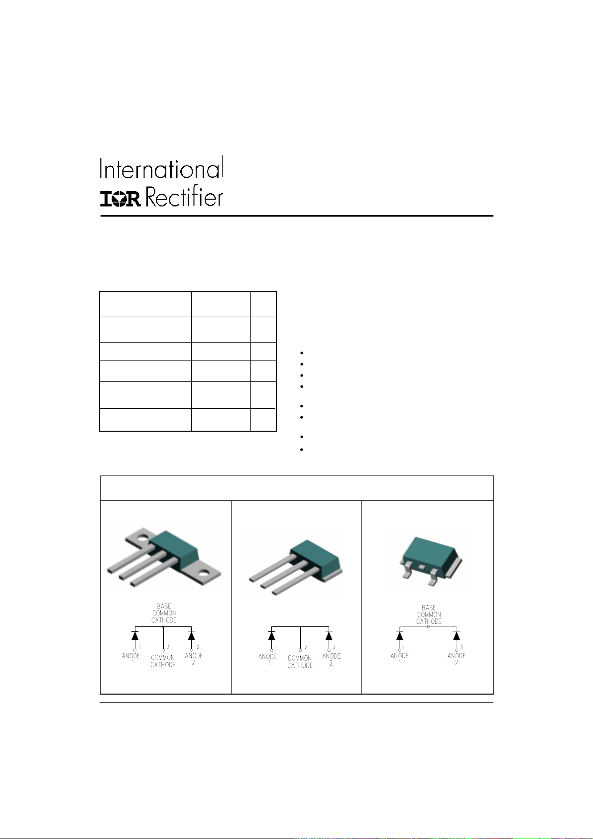
110CNQ045A
SCHOTTKY RECTIFIER
New GenIII D-61 Package
Major Ratings and Characteristics
Characteristics 110CNQ045A Units
I
Rectangular 110 A
F(AV)
waveform
V
RRM
I
@ tp = 5 µs sine 5400 A
FSM
VF@ 55 Apk, TJ = 125 °C 0.5 V
(per leg)
TJrange - 55 to 150 °C
110CNQ045A 110CNQ045ASM 110CNQ045ASL
45 V
110 Amp
Description/Features
The 110CNQ045A center tap Schottky rectifier module has
been optimized for very low forward voltage drop, with moderate
leakage. The proprietary barrier technology allows for reliable
operation up to 150 °C junction temperature. Typical applications are in switching power supplies, converters, free-wheeling
diodes, and reverse battery protection.
150 °C TJ operation
Center tap module
Very low forward voltage drop
High purity, high temperature epoxy encapsulation for
enhanced mechanical strength and moisture resistance
High frequency operation
Guard ring for enhanced ruggedness and long term
reliability
Low profile, small footprint, high current package
New fully transfer-mold low profile, small
footprint, high current package
Case Styles
D61-8
D61-8-SM D61-8-SL
Page 3
110CNQ045A
Document Number: 93200
www.vishay.com
2
Bulletin PD-20629 rev. A 09/01
Voltage Ratings
Part number 110CNQ045A
VRMax. DC Reverse Voltage (V) 45
V
Max. Working Peak Reverse Voltage (V)
RWM
Absolute Maximum Ratings
Parameters 110CNQ Units Conditions
I
Max. Average Forward Per Leg 55 A 50% duty cycle @ TC = 125 °C, rectangular wave form
F(AV)
Current * See Fig. 5 Per Device 110
I
Max. Peak One Cycle Non-Repetitive 5400 5µs Sine or 3µs Rect. pulse
FSM
Surge Current (Per Leg) * See Fig. 7 800 10ms Sine or 6ms Rect. pulse
EASNon-Repetitive Avalanche Energy 54 mJ T
(Per Leg)
A
= 25 °C, I
J
= 8 Amps, L = 1.7 mH
AS
IARRepetitive Avalanche Current 8 A Current decaying linearly to zero in 1 µsec
(Per Leg) Frequency limited by TJ max. VA = 1.5 x VR typical
Following any rated
load condition and with
rated V
RRM
applied
Electrical Specifications
Parameters 110CNQ Units Conditions
VFMMax. Forward Voltage Drop 0.54 V @ 55A
(Per Leg) * See Fig. 1 (1) 0.7 V @ 110A
0.5 V @ 55A
0.69 V @ 110A
IRMMax. Reverse Leakage Current 3 mA TJ = 25 °C
(Per Leg) * See Fig. 2 (1) 350 mA TJ = 125 °C
CTMax. Junction Capacitance (Per Leg) 3800 pF VR = 5VDC, (test signal range 100Khz to 1Mhz) 25°C
LSTypical Series Inductance (Per Leg) 5.5 nH Measured lead to lead 5mm from package body
dv/dt Max. Voltage Rate of Change 10,000 V/ µs
(Rated VR)
TJ = 25 °C
TJ = 125 °C
VR = rated V
(1) Pulse Width < 300µs, Duty Cycle <2%
R
Thermal-Mechanical Specifications
Parameters 110CNQ Units Conditions
TJMax. Junction Temperature Range -55 to 150 °C
T
Max. Storage Temperature Range -55 to 150 °C
stg
R
Max. Thermal Resistance Junction 0.5 °C/W DC operation * See Fig. 4
thJC
to Case (Per Leg)
R
Max. Thermal Resistance Junction 0.25 °C/W DC operation
thJC
to Case (Per Package)
R
Typical Thermal Resistance, Case 0.30 °C/W Mounting surface , smooth and greased
thCS
to Heatsink (D61-8 Only) Device flatness < 5 mils
wt Approximate Weight 7.8 (0.28) g (oz.)
T Mounting Torque Min. 40 (35)
(D61-8 Only) Max. 58 (50)
Kg-cm
(Ibf-in)
Page 4

110CNQ045A
Document Number: 93200
www.vishay.com
3
Bulletin PD-20629 09/01
1000
100
(A)
F
10
Instantaneous Forward Current - I
T = 150˚C
J
T = 125˚C
J
T = 25˚C
J
1000
Tj = 150˚C
100
(mA)
R
10
1
0.1
Reverse Current - I
0.01
0 5 10 15 20 25 30 35 40 45
125˚C
100˚C
75˚C
50˚C
25˚C
Reverse Voltage - VR (V)
Fig. 2 - Typical Values Of Reverse Current
Vs. Reverse Voltage (Per Leg)
10000
Tj = 25˚C
(p F)
T
Junction Capacitance - C
1
0 0.5 1 1.5 2
1000
0 5 10 15 20 25 30 35 40 45
Forward Voltage Drop - VFM (V)
Fig. 1 - Max. Forward Voltage Drop Characteristics
(Per Leg)
Fig. 3 - Typical Junction Capacitance
Vs. Reverse Voltage (Per Leg)
1
D = 0.75
D = 0.50
0.1
D = 0.33
D = 0.25
(°C/W)
thJC
D = 0.20
Single Pulse
0.01
(Thermal Resistance)
Notes:
1. Duty factor D = t 1 / t 2
Thermal Impedance - Z
0.001
0.00001 0.0001 0.001 0.01 0.1 1 10
2. Peak Tj = Pdm x ZthJC + Tc
t1 , Rectangular Pulse Duration (Seconds)
Fig. 4 - Max. Thermal Impedance Z
Characteristics (Per Leg)
thJC
Reverse Voltage - VR (V)
P
DM
t
1
t
2
Page 5

110CNQ045A
C
M
Document Number: 93200
www.vishay.com
4
Bulletin PD-20629 rev. A 09/01
150
140
130
120
Square wave (D = 0.50)
80% Rated Vr applied
110
see note (2)
Allowable Case Temperature (°C)
100
0 102030405060708090
Average Forward Current - I
Fig. 5 - Max. Allowable Case Temperature
Vs. Average Forward Current (Per Leg)
10000
(A)
FSM
1000
Non-Repetitive Surge Current - I
50
D = 0.75
D = 0.50
DC
40
D = 0.33
D = 0.25
D = 0.20
30
20
10
Average Power Loss (Watts)
0
0 1020304050607080
(A)
F(AV)
Fig. 6 - Forward Power Loss Characteristics
At Any Rated Load Condition
And With Rated Vrrm Applied
Following Surge
100
10 100 1000 10000
Square Wave Pulse Duration - tp (microsec)
Fig. 7 - Max. Non-Repetitive Surge Current (Per Leg)
RMS Limit
Average Forward Current - I
(Per Leg)
DC
F(AV)
(A)
L
HIGH-SPEED
SWITCH
FREE-WHEEL
DIODE
40HFL40S02
+
Vd = 25 Volt
URRENT
ONITOR
DUT
IRFP460
Rg = 25 ohm
Fig. 8 - Unclamped Inductive Test Circuit
(2) Formula used: TC = TJ - (Pd + Pd
Pd = Forward Power Loss = I
Pd
= Inverse Power Loss = VR1 x IR (1 - D); IR @ V
REV
F(AV)
) x R
REV
x VFM @ (I
;
thJC
/ D) (see Fig. 6);
F(AV)
= 80% rated V
R1
R
Page 6

Outline Table
Document Number: 93200
www.vishay.com
5
110CNQ045A
Bulletin PD-20629 09/01
Dimensions are in millimeters and (inches)
Outline D61-8-SM
Dimensions are in millimeters and (inches)
Outline D61-8
Page 7

110CNQ045A
Document Number: 93200
www.vishay.com
6
Bulletin PD-20629 rev. A 09/01
Outline Table
Dimensions are in millimeters and (inches)
Outline D61-8-SL
Marking Information
THIS IS A 110CNQ045A WITH
LOT CODE 89 09
ASSEMBLED ON WW 45, 2000
IN THE ASSEMBLY LINE "A"
INTERNATIONAL
RECTIFIER
LOGO
ASSEMBLY
LOT CODE
PART NUMBER
110CNQ045A
89 09 045A
DATE CODE
YEAR 0 = 2000
WEEK 45
LINE A
Page 8

110CNQ045A
Document Number: 93200
www.vishay.com
7
Bulletin PD-20629 09/01
Data and specifications subject to change without notice.
This product has been designed and qualified for Industrial Level.
Qualification Standards can be found on IR's Web site.
IR WORLD HEADQUARTERS: 233 Kansas St., El Segundo, California 90245, USA Tel: (310) 252-7105
TAC Fax: (310) 252-7309
09/01
 Loading...