

Page 1

6121 Baker Road,
Suite 108
Minnetonka, MN 55345
www.chtechnology.com
Phone (952) 933-6190
Fax (952) 933-6223
1-800-274-4284
Thank you for downloading this document from C&H Technology, Inc.
Please contact the C&H Technology team for the following questions -
Technical
Application
Assembly
Availability
Pricing
Phone – 1-800-274-4284
E-Mail – sales@chtechnology.com
www.chtechnology.com - SPECIALISTS IN POWER ELECTRONIC COMPONENTS AND ASSEMBLIES - www.chtechnology.com
Page 2
Bulletin I2405 rev. B 04/06
Document Number: 93689
www.vishay.com
1
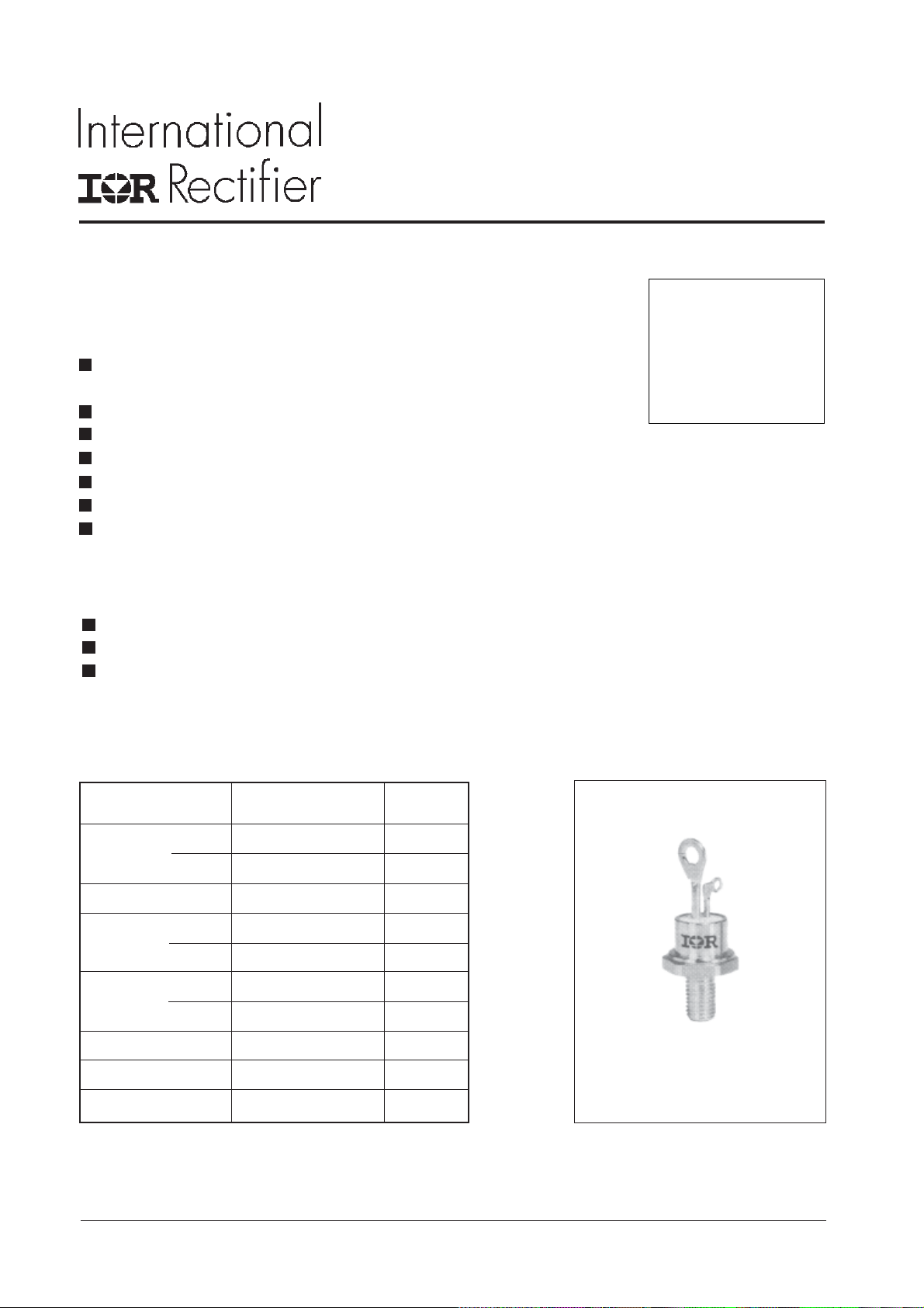
10RIA SERIES
MEDIUM POWER THYRISTORS Stud Version
Features
Improved glass passivation for high reliability
and exceptional stability at high temperature
High di/dt and dv/dt capabilities
Standard package
Low thermal resistance
Metric threads version available
Types up to 1200V V
RoHS Compliant
DRM
/ V
RRM
10A
Typical Applications
Medium power switching
Phase control applications
Can be supplied to meet stringent military,
aerospace and other high-reliability requirements
Major Ratings and Characteristics
Parameters 10RIA Unit
I
T(AV)
@ T
C
I
T(RMS)
I
TSM
2
I
t@
@ 50Hz 225 A
@ 60Hz 240 A
50Hz 255 A2s
@ 60Hz 233 A
10 A
85 °C
25 A
2
s
V
DRM/VRRM
t
q
T
J
100 to 1200 V
typical 110 μs
- 65 to 125 °C
Case Style
TO-208AA (TO-48)
Page 3
10RIA Series
Document Number: 93689
www.vishay.com
2
Bulletin I2405 rev. B 04/06
ELECTRICAL SPECIFICATIONS
Voltage Ratings
Voltage V
DRM/VRRM
Type number Code peak and off-state voltage (1) repetitive peak voltage (2)
10 100 150 20
20 200 300
40 400 500
60 600 700
10RIA 80 800 900 10
100 1000 1100
120 1200 1300
(1) Units may be broken over non-repetitively in the off-state direction without damage, if dI/dt does not exceed 20A/μs
(2) For voltage pulses with t
≤ 5ms
p
On-state Conduction
Parameter 10RIA Units Conditions
, max. repetitive V
, maximum non- I
RSM
DRM/IRRM
@ TJ = TJ max.
VVmA
max.
I
Max. average on-state current 10 A 180° conduction, half sine wave
T(AV)
@ Case temperature 85 °C
I
I
Max. RMS on-state current 25 A
T(RMS)
Max. peak, one-cycle 225 t = 10ms No voltage
TSM
non-repetitive surge current 240 t = 8.3ms reapplied
190 t = 10ms 100% V
A
RRM
200 t = 8.3ms reapplied Sinusoidal half wave,
2
t Maximum I2t for fusing 255 t = 10ms No voltage Initial TJ = TJ max.
I
233 t = 8.3ms reapplied
180 t = 10ms 100% V
A2s
RRM
165 t = 8.3ms reapplied
2
√t Maximum I2√t for fusing 2550 A2√s t = 0.1 to 10ms, no voltage reapplied
I
V
Low level value of threshold 1.10 (16.7% x π x I
T(TO)1
T(AV)
< I < π x I
), TJ = TJ max.
T(AV)
voltage
V
High level value of threshold 1.39 (I > π x I
T(TO)
2
V
), TJ = TJ max.
T(AV)
voltage
r
r
Low level value of on-state 24.3 (16.7% x π x I
t1
slope resistance
High level value of on-state 16.7 (I > π x I
t2
mΩ
T(AV)
< I < π x I
T(AV)
), TJ = TJ max.
), TJ = TJ max.
T(AV)
slope resistance
V
I
I
L
Max. on-state voltage 1.75 V Ipk= 32A, TJ = 25°C tp = 10ms sine pulse
TM
Maximum holding current 130
H
Typical latching current 200
mA
= 25°C, anode supply 12V resistive load
T
J
Page 4

Switching
Document Number: 93689
www.vishay.com
3
Parameter 10RIA Units Conditions
10RIA Series
Bulletin I2405 rev. B 04/06
di/dt Max. rate of rise of turned-on TJ = TJ max., VDM = rated V
current V
t
t
t
Typical turn-on time 0.9 TJ = 25°C,
gt
Typical reverse recovery time 4 μsTJ = TJ max.,
rr
Typical turn-off time 110 TJ = TJ max., ITM = I
q
≤ 600V 20 0 A/μs Gate pulse = 20V, 15Ω, tp = 6μs, tr = 0.1μs max.
DRM
V
≤ 800V 180 ITM = (2x rated di/dt) A
DRM
V
≤ 1000V 160
DRM
≤ 1600V 150
V
DRM
at = rated V
I
= I
TM
DRM/VRRM
, tp > 200μs, di/dt = -10A/μs
T(AV)
T(AV)
DRM
, TJ = 125°C
, tp > 200μs, VR = 100V,
di/dt = -10A/μs, dv/dt = 20V/μs linear to
67% V
, gate bias 0V-100W
DRM
(*) tq = 10μsup to 600V, tq = 30μs up to 1600V available on special request.
Blocking
Parameter 10RIA Units Conditions
dv/dt Max. critical rate of rise of 100 TJ = TJ max. linear to 100% rated V
off-state voltage 300 (*) TJ = TJ max. linear to 67% rated V
(**) Available with: dv/dt = 1000V/μs, to complete code add S90 i.e. 10RIA120S90.
V/μs
DRM
DRM
Triggering
Parameter 10RIA Units Conditions
P
Maximum peak gate power 8.0 TJ = TJ max.
GM
Maximum average gate power 2.0
P
G(AV)
Max. peak positive gate current 1.5 A TJ = TJ max.
I
GM
Maximum peak negative 10 V TJ = TJ max.
-V
GM
gate voltage
DC gate current required 90 TJ = - 65°C
I
GT
to trigger 60 mA T
DC gate voltage required 3.0 TJ = - 65°C
V
GT
to trigger 2.0 V T
I
DC gate current not to trigger 2.0 mA TJ = TJ max., V
GD
DC gate voltage not to trigger 0.2 V TJ = TJ max.
V
GD
W
35 T
1.0 V T
= 25°C
J
= 125°C
J
= 25°C
J
= 125°C
J
= rated value
V
DRM
Max. required gate trigger current/
voltage are the lowest value which
will trigger all units 6V anode-tocathode applied
= rated value
DRM
Max. gate current/ voltage not to
trigger is the max. value which
will not trigger any unit with rated
anode-to-cathode applied
V
DRM
Page 5

10RIA Series
Document Number: 93689
www.vishay.com
4
Bulletin I2405 rev. B 04/06
Thermal and Mechanical Specification
Parameter 10RIA Units Conditions
T
Max. operating temperature range - 65 to 1 25 ° C
J
T
Max. storage temperature range - 6 5 to 125 °C
stg
R
Max. thermal resistance, 1.85 K/W DC operation
thJC
junction to case
Max. thermal resistance, 0.35 K/W Mounting surface, smooth, flat and greased
R
thCS
case to heatsink
T Mounting torque to nut to device
20(27.5) 25 lbf-in Lubricated threads
0.23(0.32) 0.29 kgf.m (Non-lubricated threads)
2.3(3.1) 2.8 Nm
wt Approximate weight 14 (0.49) g (oz)
Case style TO-208AA (TO-48) See Outline Table
ΔR
(The following table shows the increment of thermal resistence R
Conduction
thJC
when devices operate at different conduction angles than DC)
thJC
Conduction angle Sinusoidal conduction Rectangular conduction Units Conditions
180° 0.44 0.32 K/W T
120° 0.53 0.56
90° 0.68 0.75
60° 1.01 1.05
30° 1.71 1.73
J
Ordering Information Table
Device Code
10 RIA 120 M S90
1 - Current code
2
1
5
43
= TJ max.
2 - Essential part number
3 - Voltage code: Code x 10 = V
(See Voltage Rating Table)
RRM
4 - None = Stud base TO-208AA (TO-48) 1/4" 28UNF-2A
M = Stud base TO-208AA (TO-48) M6 X 1
5 - Critical dv/dt: None = 300V/μs (Standard value)
S90 = 1000V/μs (Special selection)
Page 6

Outline Table
Document Number: 93689
www.vishay.com
5
10RIA Series
Bulletin I2405 rev. B 04/06
130
120
110
100
90
80
70
60
50
Maximum Allowable Case Temperature (°C)
40
0 2 4 6 8 1012141618
10RIA Series
R (DC) = 1.85 K/W
thJC
Conducti on Angl e
30°
60°
90°
120°
Average On-state Current (A)
Fig. 1 - Current Ratings Characteristic Fig. 2 - Current Ratings Characteristic
180°
Case Style TO-208AA (TO-48)
All dimensions in millimeters (inches)
130
120
110
100
90
80
70
60
50
Maximum Allowable Case Temperature (°C)
40
0 5 10 15 20 25 30
10RIA Series
R (DC) = 1.85 K/W
thJC
30°
60°
90°
120°
Average On-state Current (A)
Conducti on Peri od
180°
DC
Page 7

10RIA Series
Document Number: 93689
www.vishay.com
6
Bulletin I2405 rev. B 04/06
35
180°
30
25
20
15
10
5
Maximum Average On-state Power Loss (W)
0
120°
90°
60°
30°
RMS Limi t
024681012141618
Average On-state Current (A)
R
t
h
S
A
=
1
K
/
W
D
Conduct ion Angle
10RIA Series
T = 125°C
J
2
K
/
W
3
K
/
W
4
K
/
W
5
K
/
W
7
K
/
W
1
0
K
/
W
0 255075100125
Maximum Allowable Ambient Temperature (°C)
Fig. 3 - On-state Power Loss Characteristics
e
l
t
a
R
45
DC
40
180°
120°
35
30
90°
60°
30°
25
20
RMS Limit
15
10
5
Maximum Average On-state Power Loss (W)
0
Conducti on Period
10RIA Series
T = 125°C
J
0 5 10 15 20 25 30
Average On-state Current (A)
Fig. 4 - On-state Power Loss Characteristics
200
190
180
170
At Any Rated Load Condition And With
Rated V Applied Foll owing Surge.
RRM
Initial T = 125°C
J
@ 60 Hz 0.0083 s
@ 50 Hz 0.0100 s
160
150
140
130
120
110
10RIA Series
100
Peak Half Sine Wave On-state Current (A)
90
1 10 100
Number Of Equal Amplitude Half Cycle Current Pul ses (N)
R
t
h
S
A
=
1
K
/
2
K
/
3
K
/
W
4
K
/
W
5
K
/
W
7
K
/
W
1
0
K
W
-
W
/
W
D
e
l
t
a
R
0 25 50 75 100 125
Maximum All owable Ambient Temperature (°C)
240
220
200
180
Maximum Non Repetitive Surge Current
Versus Pulse Train Duration. Control
Of Conduction May Not Be Maintained.
No Voltage Reapplied
Rated V Reapplied
160
140
120
10RIA Series
100
Peak Half Sine Wave On-state Current (A)
80
0.01 0.1 1
Pulse Train Durati on (s)
Initial T = 125°C
J
RRM
Fig. 5 - Maximum Non-Repetitive Surge Current
Fig. 6 - Maximum Non-Repetitive Surge Current
Page 8

1000
Document Number: 93689
www.vishay.com
7
10RIA Series
Bulletin I2405 rev. B 04/06
thJC
10
Steady State Value
R = 1.85 K/W
thJC
(DC Operation)
1
100
T = 25°C
J
T = 1 2 5 °C
J
10
Instantaneous On-state Current (A)
10RIA Series
1
0.5 1 1.5 2 2.5 3 3.5 4
Instantaneous On-state Voltage (V)
Fig. 7 - Forward Voltage Drop Characteristics
10RIA Series
Transient Thermal Impedance Z (K/W)
0.1
0.001 0.01 0.1 1 10
Square Wave Pulse Duration (s)
Fig. 8 - Thermal Impedance Z
100
Rectan gular gate pulse
a) Recommended load li ne for
rated di/dt : 10V, 20ohms
tr <=0.5 µs, tp >= 6 µs
b) Recommended load line for
<=30% rated di/dt : 10V, 65ohms
10
tr<=1 µs, tp >= 6 µs
(b)
Tj = -65 ° C
Tj = 25 °C
1
Instantaneous Gate Voltage (V)
VGD
IGD
0.1
0.001 0.01 0.1 1 10 100
Tj = 125 °C
Instantaneous Gate Current (A)
(a)
10RIA Series Frequency Limited by PG(AV)
Characteristics
thJC
(1) PGM = 16W, tp = 4ms
(2) PGM = 30W, tp = 2ms
(3) PGM = 60W, tp = 1ms
(4) PGM = 60W, tp = 1ms
(1)
(2)
(3)
(4)
Fig. 9 - Gate Characteristics
Page 9

10RIA Series
Document Number: 93689
www.vishay.com
8
Bulletin I2405 rev. B 04/06
IR WORLD HEADQUARTERS: 233 Kansas St., El Segundo, California 90245, USA Tel: (310) 252-7105
Data and specifications subject to change without notice.
This product has been designed and qualified for Industrial and Consumer Level and Lead-Free.
Qualification Standards can be found on IR's Web site.
TAC Fax: (310) 252-7309
03/06
 Loading...