

Page 1

ACTIVE MODULE
CARRIER
USER’S MANUAL
MODEL
VX402C-64
C&H Technologies, Inc. <> 445 Round Rock West Drive <> Round Rock, TX 78681 <> www.chtech.com
Document Part No: 11028504B
Page 2

COPYRIGHT
C&H Technologies, Inc. (C&H) provides this manual "as is" without warranty of any kind, either
expressed or implied, including but not limited to the implied warranties of merchantability and fitness
for a particular purpose. C&H may make improvements and/or changes in the product(s) and/or
program(s) described in this manual at any time and without notice.
This publication could contain technical inaccuracies or typographical errors. Changes are periodically
made to the information herein; these changes will be incorporated in new editions of this publication.
Copyright © 2002, 2008 by C&H Technologies, Inc.
The information and/or drawings set forth in this document and all rights in and to inventions disclosed
herein which might be granted thereon disclosing or employing the materials, methods, techniques or
apparatus described herein, are the exclusive property of C&H Technologies, Inc.
A Reader's Comment Form is provided at the back of this publication. If this form has been removed
address comments to:
C&H Technologies, Inc.
Technical Publications
445 Round Rock West Drive
Austin, Texas 78681-5012
Or visit our web site for support information at:
C&H Technologies, Inc. <> 445 Round Rock West Drive <> Round Rock, TX 78681 <> www.chtech.com
http://www.chtech.com.
C&H may use or distribute any of the information you supply in any way that it believes appropriate without incurring any obligations.
.
ii
Page 3

AMENDMENT NOTICE
C&H Technologies, Inc. makes every attempt to provide up-to-date manuals with the associated
equipment. Occasionally, changes are made to the equipment wherein it is necessary to provide
amendments to the manual. If any amendments are provided for this manual they are printed on colored
paper and will be provided with the module and manual. Manual updates may also be found on out web
site at www.chtech.com.
NOTE
The contents of any amendment may affect operation, maintenance, or
calibration of the equipment.
REVISION HISTORY
Rev Date Description
* 03-20-2002 Original release
A 09-13-2004 Corrected Figure A-3 (J1) & A-4 (J2) Pin Configurations
B 07-10-2008 Added -0003 and -0004 version information
Clarified Electrical information (Section 1.2.2)
Clarified Pass-Through Cable information (Section 3.3.3)
C&H Technologies, Inc. <> 445 Round Rock West Drive <> Round Rock, TX 78681 <> www.chtech.com
iii
Page 4

INTRODUCTION
This manual describes the operation and use of the C&H Model VX402C-64 VXI Active Carrier
Module (Part Number 11028500 Revision B or higher). This VXI module is one of a number of
test and data acquisition/control modules in the VME and VXI format provided by C&H.
Contained within this manual are the physical and electrical specifications, installation and
startup procedures, functional description, and configuration guidelines to adequately use the
product.
The part numbers covered by this manual are:
Part Number Description
11028500-0001 VX402C-64 (with +3.3V supplied from VXI +5V)
11028500-0002 VX402C-64 (without +3.3V supply)
11028500-0003 VX402C-64 (with +3.3V supplied from VXI -24V)
11028500-0004 VX402C-64 (with +3.3V supplied from VXI +24V)
C&H Technologies, Inc. <> 445 Round Rock West Drive <> Round Rock, TX 78681 <> www.chtech.com
iv
Page 5

TABLE OF CONTENTS
1.0 GENERAL DES CRIPTION ..................................................................................................... 7
1.1 PURPOSE OF EQUIPMENT........................................................................................ 7
1.2 S PECIFICATIONS OF EQUIPMENT.......................................................................... 8
1.2.1 Key Features .................................................................................................. 8
1.2.2 Electrical ........................................................................................................ 8
1.2.3 Mechanical................................................................................................... 10
1.2.4 Environmental.............................................................................................. 10
1.2.5 Bus Compliance ........................................................................................... 10
2.0 INSTALLATION.................................................................................................................... 11
2.1 UNPACKING AND INSPECTION............................................................................ 11
2.2 HAND LING PRECAUTIONS.................................................................................... 11
2.3 INSTALLATION........................................................................................................ 11
2.4 PREPARATION FOR RESHIPMENT....................................................................... 11
3.0 FUNCTIONAL DESCRIPTION............................................................................................. 13
3.1 GENERAL.................................................................................................................. 13
3.2 TRIGGERS.................................................................................................................. 14
3.2.1 TTL TRIGGERS.......................................................................................... 14
3.2.2 ECL TRIGGERS.......................................................................................... 15
3.3 CONNECTORS........................................................................................................... 15
3.3.1 VXI REAR Connectors................................................................................ 15
3.3.2 VME-64 FRONT CONNECTORS............................................................... 15
3.3.3 PASS-THROUGH CONNECTORS............................................................. 16
3.4 S UMBUS CONFIGURATION.................................................................................... 18
3.4.1 S UMBUS CUSTOM AREA ......................................................................... 18
3.4.2 S UMBUS JUMPER S ETTINGS................................................................... 19
4.0 OPERATING INSTRUCTIONS............................................................................................. 21
APPENDIX A - CONNECTORS................................................................................................ A-1
C&H Technologies, Inc. <> 445 Round Rock West Drive <> Round Rock, TX 78681 <> www.chtech.com
v
Page 6

LIST OF FIGURES
Figure 1. Front Panel and Top View (Top Shield Not Shown) .......................................................7
Figure 2. Power Schematic (-0001 version)....................................................................................8
Figure 3. Power Schematic (-0002 version)....................................................................................9
Figure 4. Power Schematic (-0003 & -0004 versions)....................................................................9
Figure 5. Functional Block Diagram.............................................................................................13
Figure 6. TTL Trigger Direction....................................................................................................14
Figure 7. ECL Trigger Direction...................................................................................................15
Figure 8. Pass-Through Connector Location................................................................................16
Figure 9. SU MBUS Custom Area..................................................................................................18
Figure 10. SUMBUS Jumper Settings............................................................................................19
LIST OF TABLES
Table I. Power Supply Capabilities...............................................................................................10
Table II. VXI/VME Pass-Through Connections ...........................................................................17
C&H Technologies, Inc. <> 445 Round Rock West Drive <> Round Rock, TX 78681 <> www.chtech.com
vi
Page 7
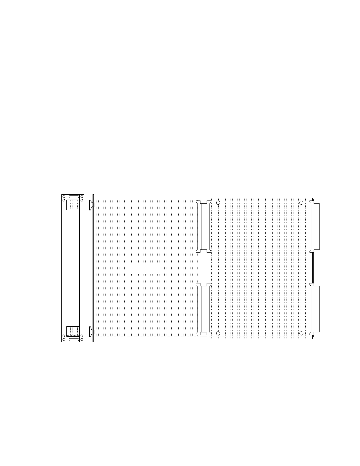
1.0 GENERAL DESCRIPTION
J1
P2 P1 P2
The VX402C-64 Active Carrier allows an A- or B-size VME, VXI, or VME64 module to be used
in a C-size VXI mainframe chassis. Throughout the rest of this manual, the VME/VXI card being
carried will be referred to as the VME module.
The carrier provides an actively-buffered electrical interface for the standard VME bus signals.
The VX402C-64 does not support the full VME64 extension bus; however, -0001, -0003, and
-0004 versions provide +3.3V power to the P1 row D VME64 extension. The adapter also
features a VXI C-size mechanical enclosure to support and shield the VME module. The carrier
and its enclosure have been designed so that the front panel of the VME module sits flush with
the front panels of other C-size modules as shown in Figure 1.
The VX402C-64 supports interrupts and provides a capability for bringing P2 VME signals to the
front panel. The carrier also supports VXI VXITTL triggers and a prototype area is provided for
buffering the VXI SUMBUS signal. These features allow the VME module to transparently
interface to a C-size chassis.
VME
USER’S VME
MODULE
USER’S VME MODULE
J2
VME
VX402C-64
Figure 1. Front Panel and Top View (Top Shield Not Shown)
C&H Technologies, Inc. <> 445 Round Rock West Drive <> Round Rock, TX 78681 <> www.chtech.com
1.1 PURPOSE OF EQUIPMENT
This VX402C-64 was designed to provide an interface for using B-size VME modules in a VXI
C-size chassis. The active nature of the module allows extensions of the VXI bus without
violation of VME/VXI electrical bus standards.
P1
7
Page 8

1.2 S PECIFICATIONS OF EQUIPMENT
+5V +3.3V
+5V
GND
GND
1.2.1 Key Features
Provides direct access to the VME module’s front panel I/O connections
Supplies buffered data, address, interrupt, and trigg er lines (ECL and TTL)
Includes direct SUMBUS connections, as well as a prototypi ng area with fused ±12V
power supplies for buffered SUMBUS connections (jumper selectable)
Conforms with VMEbus/VXIbus driving and loading specifications
Provides VME64 +3.3V supplies (-0001, -0003, and -0004 versions only)
Mates with VXI, VME, and VME64 rear connectors
1.2.2 Electrical
The -0001, -0003, and -0004 versions provide +3.3V power to the P1 row D VME64 extension.
The -0002 version does not provide +3.3V power. A simplified power schematic for each
version is shown in Figure 2, Figure 3, and Figure 4. Excluding the +3.3V supply, the VX402C64 only requires 300mA of +5V power from the VXI backplane. This power requirement is for
the VX402C-64 alone. Any attached module will increase this value by the amount specified in
its data sheet.
Table I provides a summary of the supply capabilities of each version. The table assumes that
the VXI backplane is capable providing 1.2A on each of the seven +5V power pins. For versions
-0003 and -0004, 1.2A on the -24V and +24V pins.
VXI
BACKPLANE
(7 PINS)
INTERNAL
LOGIC
C&H Technologies, Inc. <> 445 Round Rock West Drive <> Round Rock, TX 78681 <> www.chtech.com
DC-DC
CONVERTER
VME64
CONNECTORS
(7 PINS)
(10 PINS)
Figure 2. Power Schematic (-0001 version)
8
Page 9

+5V +5V
GND
GND
+5V +3.3V
+5V
GND
GND
+24V or
-
24V
CONVERTER
VXI
BACKPLANE
(7 PINS)
INTERNAL
LOGIC
VME64
CONNECTORS
(7 PINS)
Figure 3. Power Schematic (-0002 version)
VXI
BACKPLANE
VME64
CONNECTORS
(7 PINS)
(1 PIN)
INTERNAL
LOGIC
ISOLATED
DC-DC
OUT-
OUT+
(7 PINS)
(10 PINS)
Figure 4. Power Schematic (-0003 & -0004 versions)
C&H Technologies, Inc. <> 445 Round Rock West Drive <> Round Rock, TX 78681 <> www.chtech.com
9
Page 10

Table I. Power Supply Capabilities
VX402C-64 Version
-0001 -0002 -0003 -0004
VXI +5V Supply Capability 42.0W 42.0W 42.0W 42.0W
VXI +24V Supply Capability not used not used not used 29W
VXI -24V Supply Capability not used not used 29W not used
Internal +5V Power Consumption 1.5W 1.5W 1.5W 1.5W
Remaining +5V Power Available 40.5W 40.5W 40.5W 40.5W
+3.3V Converter Efficiency 92% n/a 80% 80%
+5V Power Available to VME Module 40.5W 40.5W 40.5W
+3.3V Power Available to VME Module
37W Total
0W 23W 23W
n/a = not applicable
1.2.3 Mechanical
The mechanical dimensions of the VX402C-64 are in conformance with the VXI bus
specification for the height and width of Size-C modules. The nominal dimensions are 233.35
mm (9.187 in) high x 156.337 mm (6.155 in) deep. Once the VX402C-64 is adapted to a VME
module, the total dimensions are 233.35 mm (9.187 in) high x 340.0 mm (13.386 in) deep. The
module is designed for a mainframe with 30.48 mm (1.2 in) spacing between slots.
1.2.4 Environmental
The environmental specifications of the module are:
Operating Temperature: 0C to +55C
Storage Temperature: -40C to +75C
Humidity: <95% without condensation
1.2.5 Bus Compliance
The module complies with the VXIbus Specification Revision 1.4 and with VMEbus
Specification ANSI/IEEE STD 1014-1987, IEC 821 and IEC 822.
Module: VME to VXI Extender
C&H Technologies, Inc. <> 445 Round Rock West Drive <> Round Rock, TX 78681 <> www.chtech.com
Device Type: Active Carrier
10
Page 11

2.0 INSTALLATION
2.1 UNPACKING AND INSPECTION
In most cases the VX402C-64 is individually sealed and packaged for shipment. Verify that there
has been no damage to the shipping container. If damage exists then the container should be
retained as it will provide evidence of carrier caused problems. Such problems should be
reported to the carrier immediately as well as to C&H. If there is no damage to the shipping
container, carefully remove the module from its box and anti static bag and inspect for any signs
of physical damage. If damage exists, report immediately to C&H.
2.2 HAND LING PRECAUTIONS
The VX402C-64 contains components that are sensitive to electrostatic discharge. When
handling the module for any reason, do so at a static-controlled workstation, whenever possible.
At a minimum, avoid work areas that are potential static sources, such as carpeted areas. Avoid
unnecessary contact with the components on the module.
2.3 INSTALLATION
CAUTION: Read the entire User's Manual before proceeding with the
installation and application of power.
If necessary, remove the shield from the VX402C-64 and configure the switches and jumpers.
Replace the shield and insert the carrier into the appropriate slot according to the desired priority.
Insert the VME module through the front panel of the VX402C-64. Push firmly until the VME
module’s rear connectors are fully inserted into the front connector of the VX402C-64. Apply
power. If no obvious problems exist, proceed to communicate with the VME module.
The VX402C-64 connectors require high insertion force to completely connect with the VME
module. If it is difficult to assemble the unit through the front panel, it is recommended that the
VX402C-64 shield be removed, and the boards be mated before insertion into the chassis.
2.4 PREPARATION FOR RESHIPMENT
If the module is to be shipped separately it should be enclosed in a suitable water and vapor proof
anti static bag. Heat seal or tape the bag to insure a moisture-proof closure. When sealing the
C&H Technologies, Inc. <> 445 Round Rock West Drive <> Round Rock, TX 78681 <> www.chtech.com
bag, keep trapped air vol ume to a minimum.
The shipping container should be a rigid box of sufficient size and strength to protect the
equipment from damage. If the module was received separately from a C&H system, then the
original module shipping container and packing material may be re-used if it is still in good
condition.
11
Page 12

C&H Technologies, Inc. <> 445 Round Rock West Drive <> Round Rock, TX 78681 <> www.chtech.com
12
Page 13

3.0 FUNCTIONAL DESCRIPTION
3.1 GENERAL
VX402C-64 is a general purpose carrier module for VXI C-Size chasses. The module provides
actively buffered signals, which meet all VME specifications, to the VME module. A functional
block diagram is shown in Fig ure 5.
To VME
Module
J1
J2
Pass-Through
Connectors
Trigger
Buffer
Interrupt
Buffer
Address
Buffer
Data
Buffer
Trigger
Buffer
P1
P2
To VXI
Backplane
Figure 5. Functional Block Diagram
C&H Technologies, Inc. <> 445 Round Rock West Drive <> Round Rock, TX 78681 <> www.chtech.com
13
Page 14

3.2 TRIGGERS
`
J1
P1
P2
FROM
TO
TTLTRG2
TTLTRG5
TTLTRG7
Both ECL and TTL triggers are supplied through the VX402C-64. There are switches on the
carrier which are used to set the direction of the triggers (to the backplane and from the
backplane).
3.2.1 TTL TRIGGERS
Eight TTL Trigger lines pass through the VX402C-64 to the front panel: TTLTRG0-7. Each
trigger line may be set as an input or output trigger. The trigger direction is set using switch S1
which can be seen in Figure 6. The directions are also clearly marked on the board itself.
S1
ON
1
TTLTRG0
TTLTRG1
TTLTRG3
TTLTRG4
TTLTRG6
J2
S1
BACKPLANE
BACKPLANE
TTLTRG
Figure 6. TTL Trigger Direction
C&H Technologies, Inc. <> 445 Round Rock West Drive <> Round Rock, TX 78681 <> www.chtech.com
14
Page 15
3.2.2 ECL TRIGGERS
J1
J2
P1
P2
S2
FROM
TO
S2
ECL
TRG
ECL
TRG0
ECL
TRG1
The VX402C-64 supports two ECL Trigger lines: ECLTRG0-1. Each trigger line may be set as
an input or output trigger. The trigger direction is set using switch S2 which can be seen in Figure
7. The trigger directions are clearly marked on the board itself.
ON
1
BACKPLANE
BACKPLANE
Figure 7. ECL Trigger Direction
3.3 CONNECTORS
3.3.1 VXI REAR Connectors
The P1 and P2 connectors are configured in accordance with the VXI specification and utilize
the ECL and TTL trigger lines. Pinout details for the rear connectors can be found in Appendix
A.
3.3.2 VME-64 FRONT CONNECTORS
C&H Technologies, Inc. <> 445 Round Rock West Drive <> Round Rock, TX 78681 <> www.chtech.com
The VX402C-64 interfaces with the VME module through two 160 pin VME-64 connectors: J1
and J2. These connectors conform to VME and VXI specifications and can accept both 160 pin
VME-64 (DIN 41 612 type C) and standard 96 pin VME/VXI connectors. Pinout details for the
front connectors can be found in Appendix A.
15
Page 16
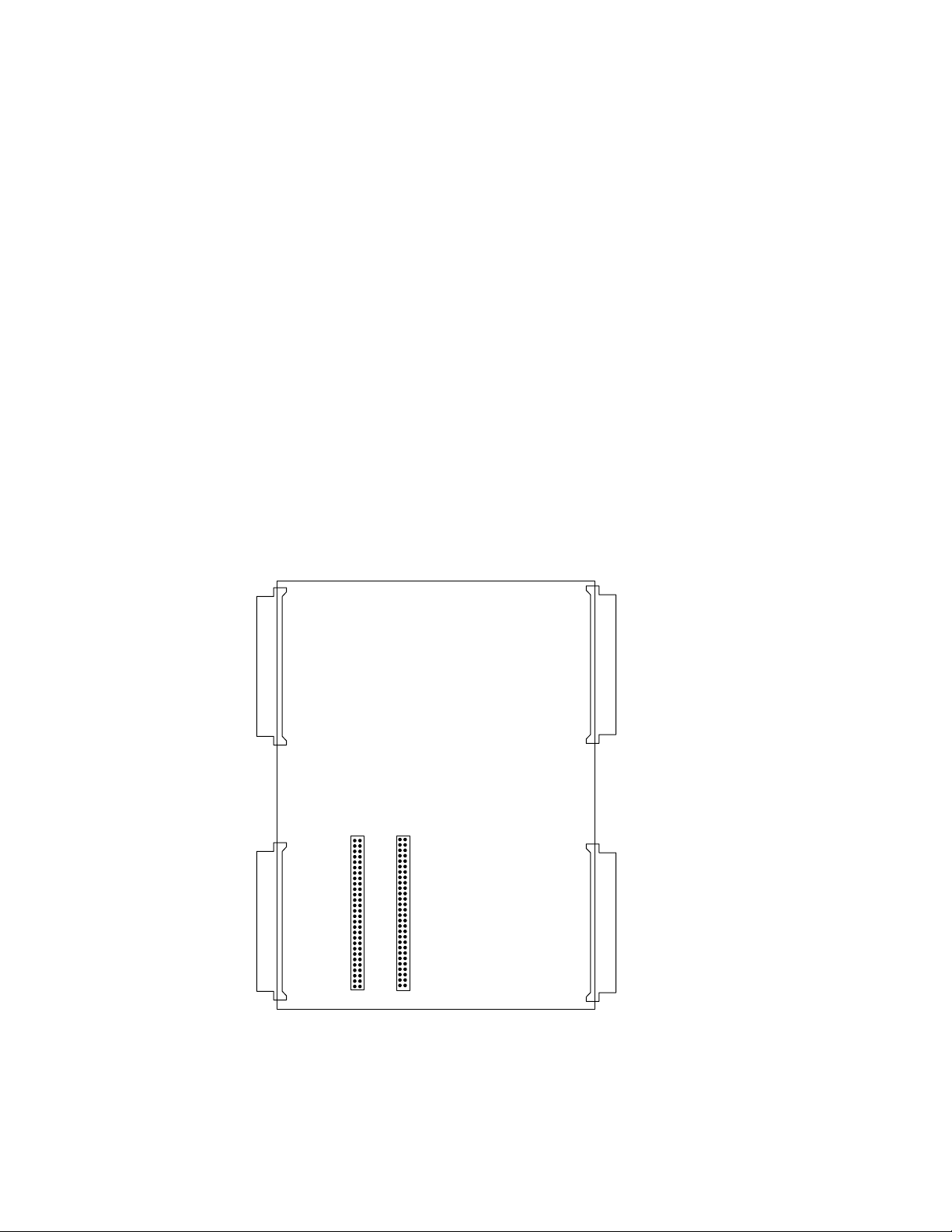
3.3.3 PASS-THROUGH CONNECTORS
J1
P1 P2
J11 J12
One major difference between the VME bus and the VXI bus is that the outer rows of the P2
connector are not defined on the VME bus and they are defined on the VXI bus. For this reason,
the VX402C-64 Active Module Carrier provides a Pass-Through Connector system that be used
to optionally connect or not connect the VME P2 Rows A & C signals to the VXI P2 Rows A &
C signals.
The VX402C-64 can be shipped with an optional pass-through connector cable (11028508-
0001). This cable is used to make internal connections between the P2 and J2 connectors on the
VX402C-64. When the cable is installed, signals on the J2 connector of the VME module are
routed to signals on the P2 connector of the backplane. Only use this cable for modules which
utilize the outer rows on the J2 connector and completely adhere to the VXI specification. If the
VME module has no outer row connections, it is unnecessary to install the cable.
If the VME module has P2 signals which do not conform to the VXI spec, it may be necessary to
make a custom pass-through cable. Also, if the VME module does not support the outer row of
the J2 connector, a longer cable may be used to directly access these signals. Pinout details for
the pass-through connectors can be found in Appendix A. Figure 8 shows the placement of the
pass-through connectors on the VX402C-64.
Pass-Through
Connectors
To J2 Front
Connector
J2
C&H Technologies, Inc. <> 445 Round Rock West Drive <> Round Rock, TX 78681 <> www.chtech.com
To P2 Rear
Connector
Figure 8. Pass-Through Connector Location
16
Page 17

A one-to-one cable that connects Pin 1 (C32) on the VXI side to Pin 1 (C32) on the VME side,
and so on, could only be used if the VME module was designed to meet all of the VXI bus
specifications for these pins. If the installed VME module can not handle -24V, +24V, -5.2V or
any other signal on the corresponding pin, then a one-to-one cable can not be used.
The signal list for both the VXI side and the VME side is shown in Table II. The pass-through
connectors on the PCB are standard 64-pin (32x2) shrouded headers, specifically Samtec TST132-01-S-D. Mating connectors are very common in both IDC and discreet wire varieties.
Table II. VXI/VME Pass-Through Connections
VXI SIDE PASS-THROUGH CONNECTOR
VME SIDE PASS-THR OUGH CONNECTOR
PI N P2 SIGNAL PIN P2 SIGNAL PIN P2 SIGNAL PIN P2 SIGNAL
1
11
13
15
17
19
21
23
25
27
29
31
33
35
37
39
41
43
45
47
49
51
53
55
57
59
61
63
C32
3
C31
5
C30
7
C29
9
C28
C27
C26
C25
C24
C23
C22
C21
C20
C19
C18
C17
C16
C15
C14
C13
C12
C11
C10
C9
C8
C7
C6
C5
C4
C3
C2
C1
-24V
+24V
GND
RSV3
GND
TTLTRG7*
TTLTRG5*
GND
TTLTRG3*
TTLTRG1*
GND
LBUSC11
LBUSC10
-5.2V
LBUSC09
LBUSC08
GND
LBUSC07
LBUSC06
-2V
LBUSC05
LBUSC04
GND
LBUSC03
LBUSC02
GND
LBUSC01
LBUSC00
-5.2V
GND
CLK10CLK10+
2
4
6
8
10
12
14
16
18
20
22
24
26
28
30
32
34
36
38
40
42
44
46
48
50
52
54
56
58
60
62
64
A32
A31
A30
A29
A28
A27
A26
A25
A24
A23
A22
A21
A20
A19
A18
A17
A16
A15
A14
A13
A12
A11
A10
A9
A8
A7
A6
A5
A4
A3
A2
A1
SUMBUS
GND
MODID
RSV2
GND
TTLTRG6*
TTLTRG4*
+5V
TTLTRG2*
TTLTRG0*
GND
LBUSA11
LBUSA10
-5.2V
LBUSA09
LBUSA08
GND
LBUSA07
LBUSA06
-5.2V
LBUSA05
LBUSA04
GND
LBUSA03
LBUSA02
-5.2V
LBUSA01
LBUSA00
GND
ECLTRG1
-2V
ECLTRG0
1
3
5
7
9
11
13
15
17
19
21
23
25
27
29
31
33
35
37
39
41
43
45
47
49
51
53
55
57
59
61
63
C32
C31
C30
C29
C28
C27
C26
C25
C24
C23
C22
C21
C20
C19
C18
C17
C16
C15
C14
C13
C12
C11
C10
C9
C8
C7
C6
C5
C4
C3
C2
C1
USER DEF
USER DEF
USER DEF
USER DEF
USER DEF
USER DEF
USER DEF
USER DEF
USER DEF
USER DEF
USER DEF
USER DEF
USER DEF
USER DEF
USER DEF
USER DEF
USER DEF
USER DEF
USER DEF
USER DEF
USER DEF
USER DEF
USER DEF
USER DEF
USER DEF
USER DEF
USER DEF
USER DEF
USER DEF
USER DEF
USER DEF
USER DEF
2
4
6
8
10
12
14
16
18
20
22
24
26
28
30
32
34
36
38
40
42
44
46
48
50
52
54
56
58
60
62
64
A32
A31
A30
A29
A28
A27
A26
A25
A24
A23
A22
A21
A20
A19
A18
A17
A16
A15
A14
A13
A12
A11
A10
A9
A8
A7
A6
A5
A4
A3
A2
A1
USER DEF
USER DEF
USER DEF
USER DEF
USER DEF
USER DEF
USER DEF
USER DEF
USER DEF
USER DEF
USER DEF
USER DEF
USER DEF
USER DEF
USER DEF
USER DEF
USER DEF
USER DEF
USER DEF
USER DEF
USER DEF
USER DEF
USER DEF
USER DEF
USER DEF
USER DEF
USER DEF
USER DEF
USER DEF
USER DEF
USER DEF
USER DEF
C&H Technologies, Inc. <> 445 Round Rock West Drive <> Round Rock, TX 78681 <> www.chtech.com
To use the VXI TTLTRG signals, a custom cable should be used that connects each TTLTRG
signal to the desired VME P2 connector signal. The VX402C-64 has a set of eight switches that
are set to specify the direction of the trigger signal as shown Figure 6. If the trigger signal is an
input to the VME module, the switch should be ON (closed). If the trigger signal is output from
the VME module, the switch should be OFF (open).
17
Page 18
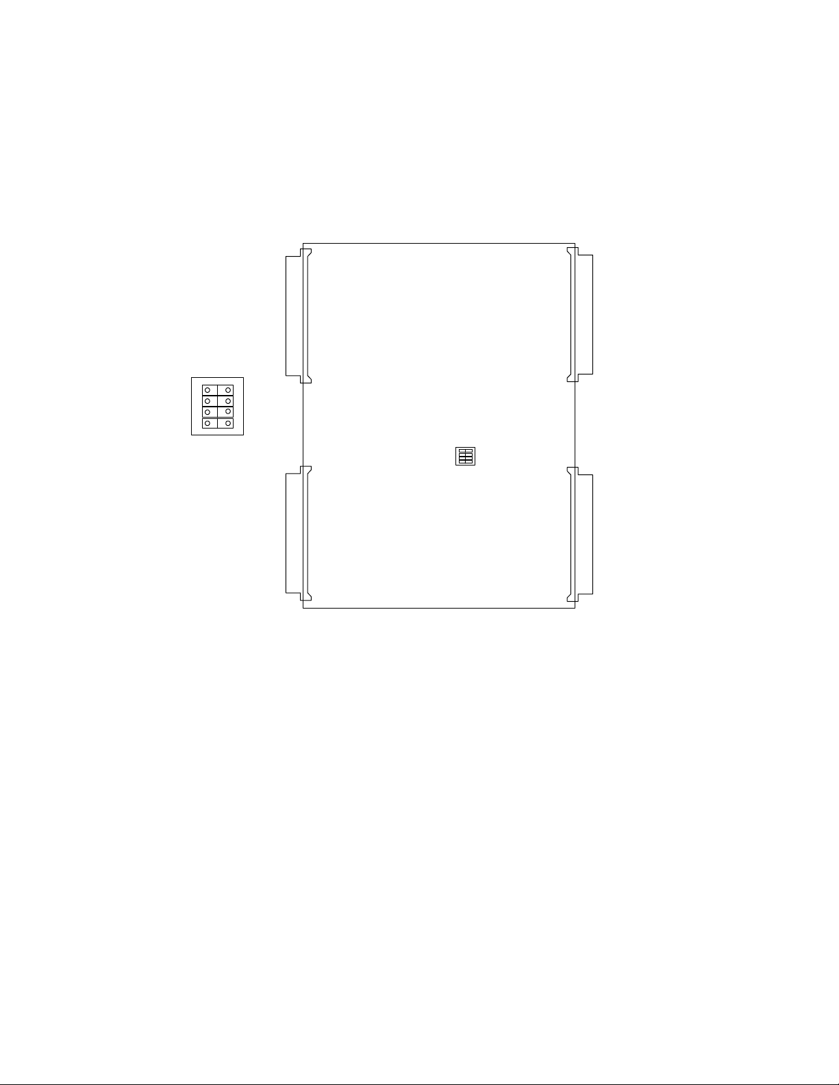
3.4 S UMBUS CONFIGURATION
J1
J2 P1 P2 SUMBUS
CUSTOM AREA
-
12V +
12V J21
The VX402C-64 provides a direct connection of the SUMBUS signal through the pass-through
connector to the front connectors. The board also has a prototyping area so that the user can
hardwire a custom buffer for the SUMBUS signal.
3.4.1 S UMBUS CUSTOM AREA
The SUMBUS custom area consists of a prototyping grid, ±12V supplies, and two jumpers for
configuring the signal. The prototyping area is a 10x10 grid of 0.1” spaced through-hole pads
which can be used in any way desired. The SUMBUS signal can be wired to the prototyping area
using the two pads next to jumpers J21 and J13, and the jumpers must be configured to the
proper setting. The location of the custom area can be seen in Figure 9.
J13
Figure 9. SUMBUS Custom Area
C&H Technologies, Inc. <> 445 Round Rock West Drive <> Round Rock, TX 78681 <> www.chtech.com
18
Page 19

3.4.2 SUMBUS JUMPER SETTINGS
J21
SUMBUS CUST DIR
J13 J21
SUMBUS CUST DIR
J13 J21
SUMBUS
CUST DIR
J13
In order to use the SUMBUS signal, the jumpers J11 and J12 must be configured properly. The
three different settings for the jumpers can be seen in Figure 10. The SUMBUS signal can be
connected directly to the front panel (A), connected through the prototyping area (B), or
disconnected (C).
The pass-through connector must be installed for the SUMBUS signal to route to the front panel.
Also, both jumpers must be configured the same, or the SUMBUS signal will be disconnected.
Direct Connection
(A)
Custom Connection
(B)
Disconnec ted
(C)
Figure 10. SUMBUS Jumper Settings
C&H Technologies, Inc. <> 445 Round Rock West Drive <> Round Rock, TX 78681 <> www.chtech.com
19
Page 20

C&H Technologies, Inc. <> 445 Round Rock West Drive <> Round Rock, TX 78681 <> www.chtech.com
20
Page 21

4.0 OPERATING INSTRUCTIONS
While the VX402C-64 is an active carrier, it is designed to be completely transparent to the host
interface. For this reason, the VME module can be accessed as if it were plugged directly into
the host backplane.
In order to operate the VME module, first set up the hardware configurations on the VX402C-64.
Then set the necessary trigger directions using the switches. Ensure the jumpers are set for proper
SUMBUS signal routing. Install or remove the pass-through connector cable as desired and
replace the shield if necessary.
The unit is now ready to be inserted into the chassis. Next, install the VME module into the front
connectors of the VX402C-64. Once power is applied, the VME module can be readily accessed
as if it were plugged directly in the backplane.
C&H Technologies, Inc. <> 445 Round Rock West Drive <> Round Rock, TX 78681 <> www.chtech.com
21
Page 22

C&H Technologies, Inc. <> 445 Round Rock West Drive <> Round Rock, TX 78681 <> www.chtech.com
22
Page 23

APPENDIX A - CONNECTORS
PIN C B A
1
2
3
4
5
6
7
8
9
10
11
12
13
14
15
16
17
18
19
20
21
22
23
24
25
26
27
28
29
30
31
32
D08
D09
D10
D11
D12
D13
D14
D15
GND
SYSFAIL*
BERR*
SYSRESET*
LWORD*
AM5
A23
A22
A21
A20
A19
A18
A17
A16
A15
A14
A13
A12
A11
A10
A09
A08
+12 V
+5 V
-
-
ACFAIL*
BGIN0*
BGOUT0*
BGIN1*
BG0UT1*
BGIN2*
BG0UT2*
BGIN3*
BGOUT3*
IRQ7*
IRQ6*
IRQ5*
IRQ4*
IRQ3*
IRQ2*
IRQ1*
+5VSTBY
-
-
-
-
AM0
AM1
AM2
AM3
GND
-
-
GND
+5 V
D00
D01
D02
D03
D04
D05
D06
D07
GND
SYSCLK
GND
DS1*
DS0*
WRITE*
GND
DTACK*
GND
AS*
GND
IACK*
IACKIN*
IACKOUT*
AM4
A07
A06
A05
A04
A03
A02
A01
-12 V
+5 V
Figure A-1. P1 Pin Configuration
NOTE: BGINx tied directly to BGOUTx
C&H Technologies, Inc. <> 445 Round Rock West Drive <> Round Rock, TX 78681 <> www.chtech.com
A-1
Page 24

PIN C B A
1
2
3
4
5
6
7
8
9
10
11
12
13
14
15
16
17
18
19
20
21
22
23
24
25
26
27
28
29
30
31
32
CLK10+
CLK10-
GND
-5.2V
LBUSC 00
LBUSC 01
GND
LBUSC 02
LBUSC 03
GND
LBUSC 04
LBUSC 05
-2V
LBUSC 06
LBUSC 07
GND
LBUSC08
LBUSC 09
-5.2V
LBUSC 10
LBUSC 11
GND
TTLTRG1*
TTLTRG3*
GND
TTLTRG5*
TTLTRG7*
GND
RSV3
GND
+24V
-24V
+5V
GND
RSV1
A24
A25
A26
A27
A28
A29
A30
A31
GND
+5V
D16
D17
D18
D19
D20
D21
D22
D23
GND
D24
D25
D26
D27
D28
D29
D30
D31
GND
+5V
ECLTRG0
-2V
ECLTRG1
GND
LBUSA00
LBUSA01
-5.2V
LBUSA02
LBUSA03
GND
LBUSA04
LBUSA05
-5.2V
LBUSA06
LBUSA07
GND
LBUSA08
LBUSA09
-5.2V
LBUSA10
LBUSA11
GND
TTLTRG0*
TTLTRG2*
+5V
TTLTRG4*
TTLTRG6*
GND
RSV2
MODID
GND
SUMBU S
Figure A-2. P2 Pin Configuration
C&H Technologies, Inc. <> 445 Round Rock West Drive <> Round Rock, TX 78681 <> www.chtech.com
A-2
Page 25

PIN D C B A Z
1
2
3
4
5
6
7
8
9
10
11
12
13
14
15
16
17
18
19
20
21
22
23
24
25
26
27
28
29
30
31
32
-
GND
-
-
-
-
-
-
-
-
-
+3.3V
-
+3.3V
-
+3.3V
-
+3.3V
-
+3.3V
-
+3.3V
-
+3.3V
-
+3.3V
-
+3.3V
-
+3.3V
GND
-
BD08
BD09
BD10
BD11
BD12
BD13
BD14
BD15
GND
BSYSFAIL*
BBERR*
BSYSRESET*
BLWORD*
BAM5
BA23
BA22
BA21
BA20
BA19
BA18
BA17
BA16
BA15
BA14
BA13
BA12
BA11
BA10
BA09
BA08
+12 V
+5 V
-
-
BACFAIL*
+5VSTBY
IN0*
OUT0*
IN1*
0UT 1*
IN2*
0UT 2*
IN3*
OUT3*
-
-
-
-
BAM0
BAM1
BAM2
BAM3
GND
-
-
GND
BIRQ7*
BIRQ6*
BIRQ5*
BIRQ4*
BIRQ3*
BIRQ2*
BIRQ1*
+5 V
BD00
BD01
BD02
BD03
BD04
BD05
BD06
BD07
GND
BSYSCLK
GND
BDS1*
BDS0*
BWRITE*
GND
BDTACK*
GND
BAS*
GND
BIACK*
BIACKIN*
BIACKOUT*
BAM4
BA07
BA06
BA05
BA04
BA03
BA02
BA01
-12 V
+5 V
-
GND
-
GND
-
GND
-
GND
-
GND
-
GND
-
GND
-
GND
-
GND
-
GND
-
GND
-
GND
-
GND
-
GND
-
GND
-
GND
Figure A-3. J1 Pin Configuration
NOTES:
1. INx tied directly to OUTx.
2. +3.3V supplied on Version -0001 only
C&H Technologies, Inc. <> 445 Round Rock West Drive <> Round Rock, TX 78681 <> www.chtech.com
A-3
Page 26

PIN D C B A Z
1
2
3
4
5
6
7
8
9
10
11
12
13
14
15
16
17
18
19
20
21
22
23
24
25
26
27
28
29
30
31
32
-
-
-
-
-
-
-
-
-
-
-
-
-
-
-
-
-
-
-
-
-
-
-
-
-
-
-
-
-
-
GND
-
CLK10+n
CLK10-n
GND14
-5.2V5
LBUSC00n
LBUSC01n
GND12
LBUSC02n
LBUSC03n
GND10
LBUSC04n
LBUSC05n
-2V1
LBUSC06n
LBUSC07n
GND08
LBUSC08n
LBUSC09n
-5.2V1
LBUSC10n
LBUSC11n
GND06
BTTLTRG1*
BTTLTRG3*
GND05
BTTLTRG5*
BTTLTRG7*
GND03
RSV3n
GND02
+24Vn
-24Vn
+5V
GND
RSV1
BA24
BA25
BA26
BA27
BA28
BA29
BA30
BA31
GND
+5V
BD16
BD17
BD18
BD19
BD20
BD21
BD22
BD23
GND
BD24
BD25
BD26
BD27
BD28
BD29
BD30
BD31
GND
+5V
BECLTRG0
-2V2
BECLTRG1
GND13
LBUSA00n
LBUSA01n
-5.2V4
LBUSA02n
LBUSA03n
GND11
LBUSA04n
LBUSA05n
-5.2V3
LBUSA06n
LBUSA07n
GND09
LBUSA08n
LBUSA09n
-5.2V2
LBUSA10n
LBUSA11n
GND07
BTTLTRG0*
BTTLTRG2*
+5Vn
BTTLTRG4*
BTTLTRG6*
GND04
RSV2n
MODIDn
GND01
BSUMBU Sn
-
GND
-
GND
-
GND
-
GND
-
GND
-
GND
-
GND
-
GND
-
GND
-
GND
-
GND
-
GND
-
GND
-
GND
-
GND
-
GND
Figure A-4. J2 Pin Configuration
NOTES:
1. Signals on Rows A & C are only connected, if the pass-through cable is installed.
2. +3.3V supplied on Version -0001 only
C&H Technologies, Inc. <> 445 Round Rock West Drive <> Round Rock, TX 78681 <> www.chtech.com
A-4
Page 27
TO FRONT CON NECTOR J2 TO REAR CONN E C TOR P2
PIN PIN PIN PIN
1
3
5
7
9
11
13
15
17
19
21
23
25
27
29
31
33
35
37
39
41
43
45
47
49
51
53
55
57
59
61
63
-24Vn
+24Vn
GND02
RSV3n
GND03
BTTLTRG7*n
BTTLTRG5*n
GND05
BTTLTRG3*n
BTTLTRG1*n
GND06
LBUSC11n
LBUSC10n
-5.2V1
LBUSC09n
LBUSC08n
GND08
LBUSC07n
LBUSC06n
-2V1
LBUSC05n
LBUSC04n
GND10
LBUSC03n
LBUSC02n
GND12
LBUSC01n
LBUSC00n
-5.2V5
GND14
CLK10-n
CLK10+n
2
4
6
8
10
12
14
16
18
20
22
24
26
28
30
32
34
36
38
40
42
44
46
48
50
52
54
56
58
60
62
64
BSUMBU Sn
GND01
MODIDn
RSV2n
GND04
BTTLTRG6*n
BTTLTRG4*n
+5Vn
BTTLTRG2*n
BTTLTRG0*n
GND07
LBUSA11n
LBUSA10n
-5.2V2
LBUSA09n
LBUSA08n
GND09
LBUSA07n
LBUSA06n
-5.2V3
LBUSA05n
LBUSA04n
GND11
LBUSA03n
LBUSA02n
-5.2V4
LBUSA01n
LBUSA00n
GND13
BECLTRG1n
-2V2
BECLTRG0n
1
3
5
7
9
11
13
15
17
19
21
23
25
27
29
31
33
35
37
39
41
43
45
47
49
51
53
55
57
59
61
63
-24V
+24V
GND
RSV3
GND
BTTLTRG7*
BTTLTRG5*
GND
BTTLTRG3*
BTTLTRG1*
GND
LBUSC11
LBUSC10
-5.2V
LBUSC09
LBUSC08
GND
LBUSC07
LBUSC06
-2V
LBUSC05
LBUSC04
GND
LBUSC03
LBUSC02
GND
LBUSC01
LBUSC00
-5.2V
GND
CLK10-
CLK10+
2
4
6
8
10
12
14
16
18
20
22
24
26
28
30
32
34
36
38
40
42
44
46
48
50
52
54
56
58
60
62
64
BSUMBU S
GND
MODID
RSV2
GND
BTTLTRG6*
BTTLTRG4*
+5V
BTTLTRG2*
BTTLTRG0*
GND
LBUSA11
LBUSA10
-5.2V
LBUSA09
LBUSA08
GND
LBUSA07
LBUSA06
-5.2V
LBUSA05
LBUSA04
GND
LBUSA03
LBUSA02
-5.2V
LBUSA01
LBUSA00
GND
BECLTRG1
-2V
BECLTRG0
Figure A-5. P2 Pin Configuration
C&H Technologies, Inc. <> 445 Round Rock West Drive <> Round Rock, TX 78681 <> www.chtech.com
A-5
Page 28

C&H Technologies, Inc. <> 445 Round Rock West Drive <> Round Rock, TX 78681 <> www.chtech.com
A-6
Page 29

N O T E S :
C&H Technologies, Inc. <> 445 Round Rock West Drive <> Round Rock, TX 78681 <> www.chtech.com
Page 30

C&H Technologies, Inc. <> 445 Round Rock West Drive <> Round Rock, TX 78681 <> www.chtech.com
Page 31

READER'S COMMENT FORM
Your comments assist us in improving the usefulness of C&H's publications; they are an
important part of the inputs used for revision.
C&H Technologies, Inc. may use and distribute any of the information that you supply in any
way that it believes to be appropriate without incurring any obligation whatsoever. You may, of
course, continue to use the information which you supply.
Please refrain from using this form for technical questions or for requests for additional
publications; this will only delay the response. Instead, please direct your technical questions to
your authorized C&H representative.
COMMENTS:
Thank you for helping C&H to deliver the best possible product. Your support is appreciated.
Sincerely,
C&H Technologies, Inc. <> 445 Round Rock West Drive <> Round Rock, TX 78681 <> www.chtech.com
F.R.Harrison
President and CEO
Page 32

INSTRUCTIONS
In its continuing effort to improve documentation, C&H Technologies, Inc. provides this form for
use in submitting any comments or suggestions that the user may have. This form may be
detached, folded along the lines indicated, taped along the loose edge (DO NOT STAPLE), and
mailed. Please try to be as specific as possible and reference applicable sections of the manual or
drawings if appropriate. Also, indicate if you would like an acknowledgment mailed to you
stating whether or not your comments were being incorporated.
NOTE: This form may not be used to request copies of documents or to request
waivers, deviations, or clarification of specification requirements on current
contracts. Comments submitted on this form do not constitute or imply
authorization to waive any portion of the referenced document(s) or to amend
contractual requirements.
(Fold along this line)
(Fold along this line)
______________________
______________________
______________________
C&H Technologies, Inc. <> 445 Round Rock West Drive <> Round Rock, TX 78681 <> www.chtech.com
C&H Technologies, Inc.
Technical Publications
445 Round Rock West Drive
Round Rock, Texas 78681
Place
Stamp
Here
 Loading...