

Page 1

Gathering ICs bit by bit and forming vast sea.
CSM92F30 Module
User's Manual
1/11 NO:CS-QR-YF-054A02
This document is exclusive property of CHIPSEA and shall not be reproduced or copied or transformed to any other format
without prior permission of CHIPSEA
Page 2
Gathering ICs bit by bit and forming vast sea.
Revision History
Revision Changes Date
REV1.0 Initial draft 2018/1/15
2/11 NO:CS-QR-YF-054A02
This document is exclusive property of CHIPSEA and shall not be reproduced or copied or transformed to any other format
without prior permission of CHIPSEA
Page 3
Gathering ICs bit by bit and forming vast sea.
Contents
Revision History ....................................................................................................................................................... 2
Contents .................................................................................................................................................................... 3
1 Product Overview ............................................................................................................................................ 4
1.1 Introduction ............................................................................................................................................... 4
1.2 Features ...................................................................................................................................................... 4
1.3 Pin Assignments and Functions ................................................................................................................. 5
2 Electrical Specifications .................................................................................................................................. 7
2.1 Absolute Maximum Ratings ...................................................................................................................... 7
2.2 DC Characteristics ..................................................................................................................................... 7
2.3 Receiver Specification ............................................................................................................................... 7
3 Package Dimensions ........................................................................................................................................ 8
4 Application Schematic ..................................................................................................................................... 9
A. Appendix A ..................................................................................................................................................... 10
A.1. Requirement of FCC KDB 996369 D03 for module certification: .............................................................. 10
3/11 NO:CS-QR-YF-054A02
This document is exclusive property of CHIPSEA and shall not be reproduced or copied or transformed to any other format
without prior permission of CHIPSEA
Page 4

Gathering ICs bit by bit and forming vast sea.
1 Product Overview
1.1 Introduction
The CSM92F30 Module is a highly integrated Bluetooth 5.0 low energy SOC module. It has 32-bit
ARM® Cortex™-M0 CPU with 512KB Flash, 138KB SRAM and an ultra-low power, high performance,
multi-mode radio. It intergrate rich feature peripheral units, programmable protocol and profile to support
BLE application, enables customer product to be built with minimum bill-of-material (BOM) cost.
1.2 Features
CPU
32-bit ARM® Cortex™-M0 CPU
Memories
512KB Flash
138KB SRAM
2.4GHz Transceiver
Compliant to Bluetooth 5.0
Single-pin antenna: no RF matching or RX/TX
switching required
Support four datarate
— 2Mbps
— 1Mbps
— 500Kbps
— 125Kbps
Sensitivity:
— -94dBm@BLE 2Mbps data rate
— -97dBm@BLE 1Mbps data rate
— -98dBm@BLE 500Kbps data rate
— -103dBm@BLE 125Kbps data rate
Low power consumption
Transmitter: 8mA@0dBm Tx power
Receiver: 8mA @sensitivity level
2μA @ Sleep Mode with 32KHz RTC
0.7μA @ OFF Mode(IO wake up only)
Oscillator
6-channel output PWM
1x quadrature decoder(QDEC)
1x I2S
1x PDM
2x I2C
1x UART
2x SPI
Support 16*18keyboard scan
1x 12bit ADC with analog PGA
8x 24bit timer
one watchdog timer
Real timer counter (RTC)
JTAG
Flexible power management
Supply voltage range 1.8V to 3.6V
Embedded buck DC-DC
Package
QFN32(4*4mm)
QFN48(5*5mm)
Application
Wearables
Beacon
Health and medical
Appliances
Internet of things (IOT)
BLE MESH
Support 16M XTAL
Interfaces
33/20 general purpose I/O pins
— Allpinscanbeconfiguredasdigital
interfaceandprogrammableIOMUX
functionmapping
— Allpinscanbeconfiguredforwake‐up
— 18pinsfortriggeringinterrupt
4/11 NO:CS-QR-YF-054A02
This document is exclusive property of CHIPSEA and shall not be reproduced or copied or transformed to any other format
without prior permission of CHIPSEA
Page 5
Gathering ICs bit by bit and forming vast sea.
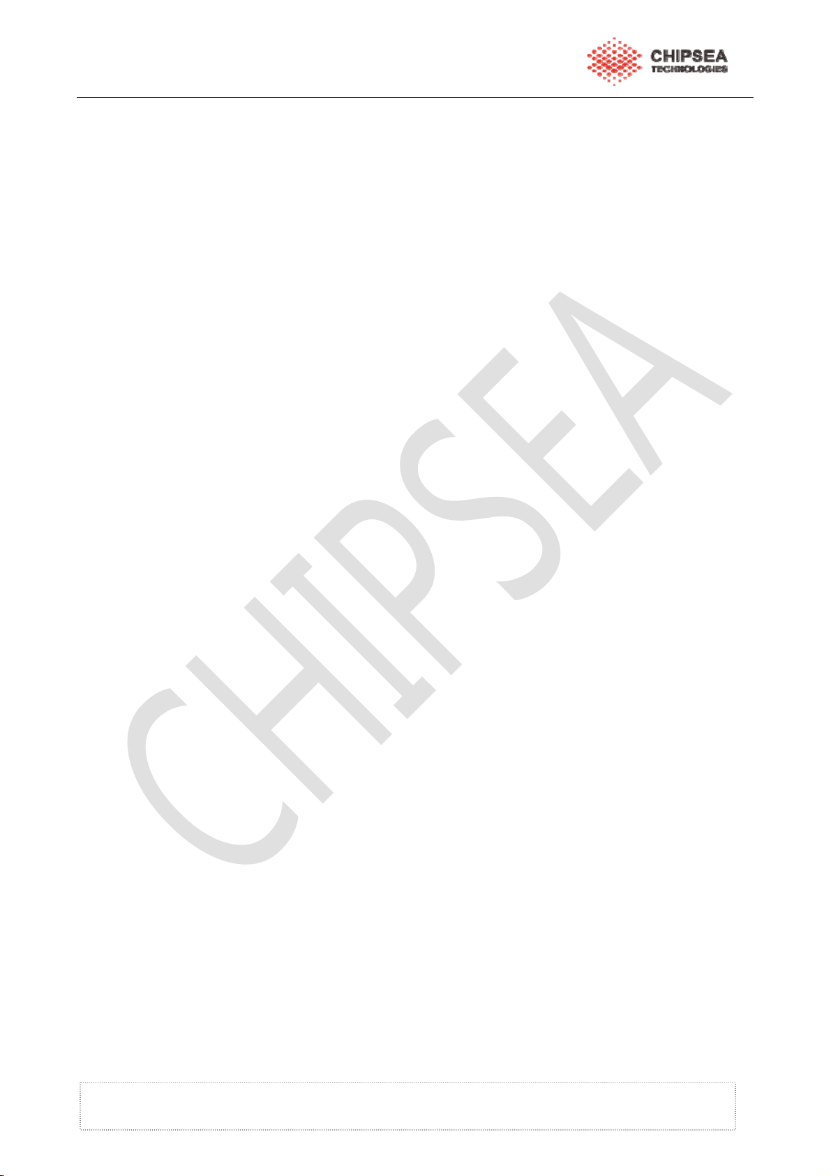
1.3 Pin Assignments and Functions
This section describes the pin assignment and the pin functions for CSM92F30 Module.
5/11 NO:CS-QR-YF-054A02
This document is exclusive property of CHIPSEA and shall not be reproduced or copied or transformed to any other format
without prior permission of CHIPSEA
Page 6
Gathering ICs bit by bit and forming vast sea.
Table 1 Pin description
QFN48
No.
1 1 P00 I/O
2 2 P01 I/O
3 3 P02 I/O
4 4 P03 I/O
9 5 BOOT0 I Boot_select[0]
20 13 P14 I/O
21 14 P15 I/O
25 18 P16 I/O
QFN32
No.
Pin name Type Description
General purpose input/output0
JTAG_TDO
General purpose input/output1
JTAG_TDI
General purpose input/outpu2
JTAG_TMS
General purpose input/output3
JTAG_TCK
General purpose input/output14
AIO3
General purpose input/output15
AIO4
General purpose input/output16
AIO5
32K crystal input
General purpose input/output17
26 19 P17 I/O
AIO6
32K crystal output
General purpose input/output18
27 20 P18 I/O
*Note: Not support interrupt function
AIO7
PGA differential positive input
General purpose input/output19
*Note: Not support interrupt function
28 21 P19 I/O
AIO8
PGA differential negative input
General purpose input/output20
29 22 P20 I/O
30 23 RST_N I
37 26 P23 I/O
38 27 P24 I/O
*Note: Not support interrupt function
AIO9
Micphone bias output
reset pin, low level active
General purpose input/output23
*Note: Not support interrupt function
General purpose input/output24
*Note: Not support interrupt function
Boot_select[1]
General purpose input/output25
39 28 P25 I/O
*Note: Not support interrupt function
Boot_select[2]
45 29 P31 I/O
46 30 P32 I/O
47 31 P33 I/O
48 32 P34 I/O
General purpose input/output31
*Note: Not support interrupt function
General purpose input/output32
*Note: Not support interrupt function
General purpose input/output33
*Note: Not support interrupt function
General purpose input/output34
*Note: Not support interrupt function
6/11 NO:CS-QR-YF-054A02
This document is exclusive property of CHIPSEA and shall not be reproduced or copied or transformed to any other format
without prior permission of CHIPSEA
Page 7
Gathering ICs bit by bit and forming vast sea.
2 Electrical Specifications
2.1 Absolute Maximum Ratings
Maximum ratings are the extreme limits to which CSM92F30 Module can be exposed
without permanently damaging it. Exposure to absolute maximum ratings for prolonged
periods of time may affect the reliability of the CSM92F30 Module.Table2 Specifies the
absolute maximum ratings for CSM92F30 Module.
Table 13 CSM92F30 Module Absolute Maximum Ratings
Symbol Range Unit
Supply voltage 0~3.6 V
I/O pin voltage -0.3~VIN+0.3 V
Operating temperature -40~+125 ºC
Storage temperature -55~+150 ºC
Solder temperature,time 220ºC,10s
2.2 DC Characteristics
Table 14 DC Characteristics
Symbol Parameter Min. Typ. Max. Unit
VIN
Supply voltage, normal
mode
1.8 3.3 3.6 V
VIH Digital input high level VIN-0.3 - VIN+0.3 V
VIL Digital input low level 0 - 0.3 V
VOH Digital output high level VIN-0.3 - VIN+0.3 V
VOL Digital output low level 0 - 0.3 V
2.3 Receiver Specification
Table 15 Receiver Specification
Parameter Min. Typ. Max. Unit
Receive sensitivity@ 125Kbps GFSK -103 dBm
Receive sensitivity @500Kbps GFSK -98 dBm
Receive sensitivity @1Mbps BLE -97 dBm
Receive sensitivity@2Mbps BLE -94 dBm
Maximum input signal level -5 dBm
7/11 NO:CS-QR-YF-054A02
This document is exclusive property of CHIPSEA and shall not be reproduced or copied or transformed to any other format
without prior permission of CHIPSEA
Page 8

Gathering ICs bit by bit and forming vast sea.
3 Package Dimensions
8/11 NO:CS-QR-YF-054A02
This document is exclusive property of CHIPSEA and shall not be reproduced or copied or transformed to any other format
without prior permission of CHIPSEA
Page 9
Gathering ICs bit by bit and forming vast sea.
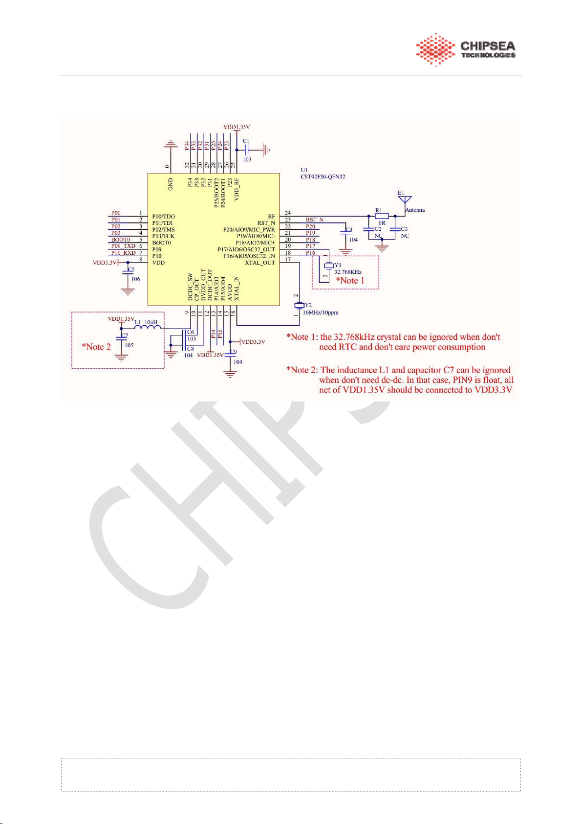
4 Application Schematic
Figure 17 CSM92F30 Module Application Schematic
9/11 NO:CS-QR-YF-054A02
This document is exclusive property of CHIPSEA and shall not be reproduced or copied or transformed to any other format
without prior permission of CHIPSEA
Page 10

Gathering ICs bit by bit and forming vast sea.
A. Appendix A
A.1. Requirement of FCC KDB 996369 D03 for module certification:
1.1 List of applicable FCC rules:
The module complies with FCC Part 15.247
1.2 Summarize the specific operational use conditions:
The module has been certified for Fix, Mobile, Portable applications. This transmitter must not be co‐located
or operating in conjunction with any other antenna or transmitter.
1.3 Limited module procedures:
The module has not its own RF shielding, which belong to Limited module Standard requires:
Clear and specific instructions describing the conditions, limitations and procedures for third‐parties to use
and/or integrate the module into a host device (see Comprehensive integration instructions below).
Resolve: Supply example as follows:
Installation Notes:
1) CSM92F30 Module Power supply range is DC 1.8V~3.6V, when you use CSM92F30 Module design
product, the power supply cannot exceed this range.
2) When connect CSM92F30 Module to the host device, the host device must be power off.
3) Make sure the module pins correctly installed.
4) Make sure that the module does not allow users to replace or demolition.
1.4 Trace antenna designs:
Not applicable.
1.5 RF exposure considerations:
This modular complies with FCC RF radiation exposure limits set forth for an uncontrolled environment.
This transmitter must not be co-located or operating in conjunction with any other antenna or transmitter.
This modular must be installed and operated with a minimum distance of 20 cm between the radiator and user
body.
Note: the host product manuals must include a statement in order to alert the users of FCC RF exposure
compliance.
1.6 Antennas:
Type Gain
PCB 0.5dBi
The antenna is permanently attached, can’t be replaced.
1.7 Label and compliance information
This device complies with part 15 of the FCC rules. Operation is subject to the
following two conditions:
(1) this device may not cause harmful interference, and (2) this device must accept any interference received,
including interference that may cause undesired operation.
Warning: Changes or modifications to this unit not expressly approved by the party responsible for
compliance could void the user’s authority to operate the equipment.
NOTE: This equipment has been tested and found to comply with the limits for a Class B digital device,
pursuant to part 15 of the FCC Rules. These limits are designed to provide reasonable protection against
harmful interference in a residential installation. This equipment generates uses and can radiate radio
10/11 NO:CS-QR-YF-054A02
Frequency Bands Modulation Mode
2402-2480 MHz
GFSK
This document is exclusive property of CHIPSEA and shall not be reproduced or copied or transformed to any other format
without prior permission of CHIPSEA
Page 11

Gathering ICs bit by bit and forming vast sea.
frequency energy and, if not installed andused in accordance with the instructions, may cause harmful
interference to radio communications. However, there is no guarantee that interference will not occur in a
particular installation. If this equipment does cause harmful interference to radio or television reception, which
can be determined by turning the equipment off and on, the user is encouraged to try to correct the interference
by one or more of the following measures:
‐ Reorient or relocate the receiving antenna.
‐ Increase the separation between the equipment and receiver.
‐Connect the equipment into an outlet on a circuit different from that to which the receiver is connected.
‐Consult the dealer or an experienced radio/TV technician for help.
The system integrator must place an exterior label on the outside of the final product housing the
2AGM5CSM92F30 Modules. Below is the content that must be included on this label.
The host product Labeling Requirements:
NOTICE: The host product must make sure that FCC labeling requirements are met. This includes clearly
visible exterior label on the outside of the final product housing that
displays the contents shown in below:
Contains FCC ID:2AGM5CSM92F30
1.8 Information on test modes and additional testing requirements:
When testing host product, the host manufacture should follow FCC KDB Publication 996369 D04 Module
Integration Guide for testing the host products. The host manufacturer may operate their product during the
measurements. In setting up the configurations, if the pairing and call box options for testing does not work,
then the host product manufacturer should coordinate with the module manufacturer for access to test mode
software
1.9 Additional testing, Part 15 Subpart B disclaimer:
The modular transmitter is only FCC authorized for the specific rule parts (FCC Part 15.247) list on the grant,
and that the host product manufacturer is responsible for compliance to any other FCC rules that apply to the
host not covered by the modular transmitter grant of certification. The final host product still requires Part 15
Subpart B compliance testing with the modular transmitter installed when contains digital circuity.
1.10 Information on test modes and additional testing requirements:
When testing host product, the host manufacture should follow FCC KDB Publication 996369 D04 Module
Integration Guide for testing the host products. The host manufacturer may operate their product during the
measurements.
11/11 NO:CS-QR-YF-054A02
This document is exclusive property of CHIPSEA and shall not be reproduced or copied or transformed to any other format
without prior permission of CHIPSEA
 Loading...