

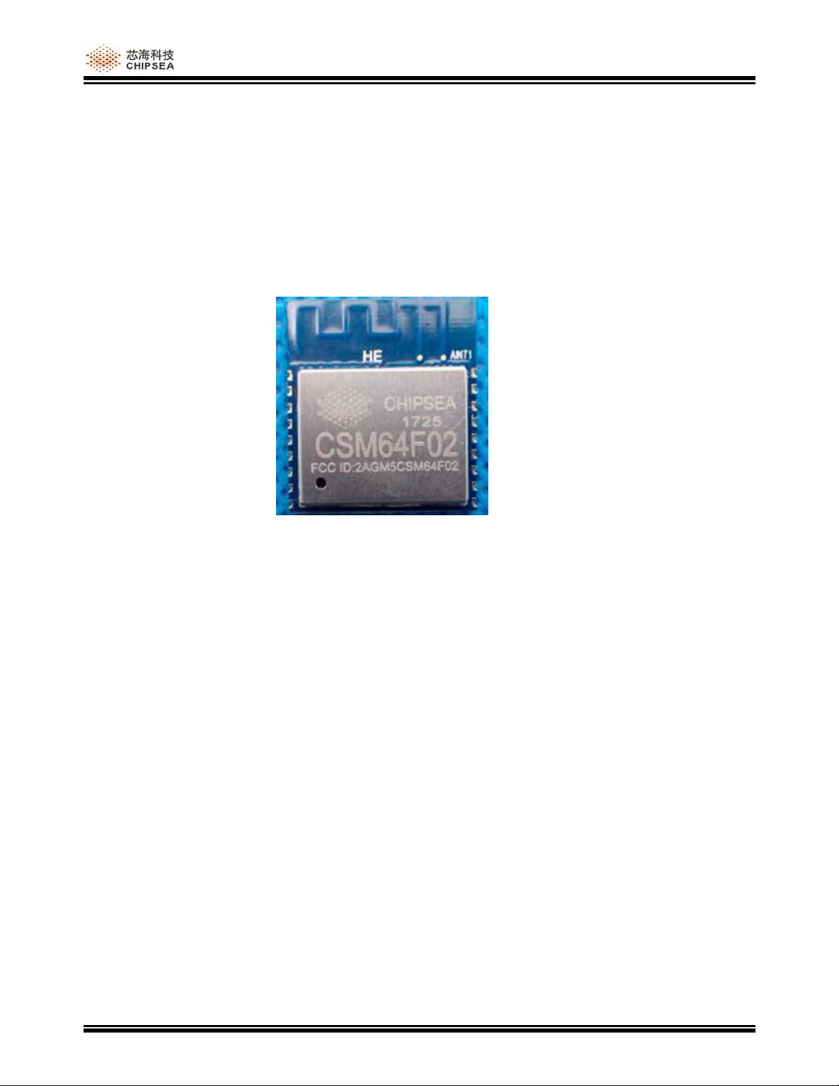
Page 1

CSM64F02 User Manual
802.11 b/g/n IoT WiFi Module
REV 1.1
Add: Floor 9, Tower A, Garden City Cyberport, No. 1079 Nanhai Avenue, Shekou Industrial Zone, Nanshan
District, Shenzhen City
Postcode: 518067
Tel: +(86 755)86169257
Fax: +(86 755)86169057
Web: www.chipsea.com
Page 2

Revision
History
Revision Date
REV 1.0
Initially issued
April 28, 2017
REV 1.1
Add Electrostatic Discharge in chapter 5.1
May 25, 2017
REV 1.2
Add FCC note at page 9
Modify lable to reduce the FCC/CE Logo
June 1, 2017
CSM64F02 User Manual
Revision History
Rev1.2 Page 2 of 13
Page 3

CSM64F02 User Manual
Contents
REVISION HISTORY ................................................................................................................................................. 2
CONTENTS ................................................................................................................................................................. 3
1 PRODUCT DESCRIPTION ................................................................................................................................ 4
1.1 FUNCTIONAL DESCRIPTION .................................................................................................................................. 4
1.2 FEATURES ............................................................................................................................................................. 4
2 PIN DEFINITION................................................................................................................................................ 5
3 REFERENCE DESIGN ....................................................................................................................................... 6
3.1 SCHEMATIC .......................................................................................................................................................... 6
3.2 PLACEMENT OF ANTENNA .................................................................................................................................... 7
3.2.1
Recommended Scheme................................................................................................................................. 7
3.2.2
Not Recommended Schemes ........................................................................................................................ 7
5 ELECTRICAL CHARACTERISTICS ............................................................................................................... 9
5.1 ABSOLUTE MAXIMUM RATIONGS ......................................................................................................................... 9
5.2 RECOMMENDED OPERATING ENVIRONMENT ........................................................................................................ 9
5.3 RF PERFORMANCE................................................................................................................................................ 9
5.4 POWER CONSUMPTION ....................................................................................................................................... 10
5.5 RAMP UP ............................................................................................................................................................. 11
6 LABEL AND ORDERING INFORMATION ................................................................................................... 12
6.1 LABEL DESCRIPTION .......................................................................................................................................... 12
6.2 ORDERING INFORMATION ................................................................................................................................... 12
7 PACKAGING INFOMATION .......................................................................................................................... 13
Rev1.2 Page 3 of 13
Page 4
CSM64F02 User Manual
1 Product Description
1.1 Functional Description
CSM64F02 is a 802.11b/g/n Wi-Fi module developed by CHIPSEA in allusion to Internet of Things. The
module integrates 32-bit high-speed CPU, TCP/IP protocol stack, RTOS, WiFi RF front end and onboard antenna,
supports ADC/ SPI/ UART/ I2C/ PWM and other IO, with small packagee and low power consumption. It can be
used widely for Internet of Things such as intelligent household electrical appliance, intelligent outlet, intelligent
health device, robot and industrial wireless control etc.
CHIPSEA provides one-stop solution including product design, APP development and IoT cloud etc. on the
basis of CSM64F02. Thus, the users may concentrate on their own creativity and application and put the products
into market rapidly.
1.2 Features
Basic feations
Built-in 32-bit ultra-low power CPU
Supporting real-time operating system (RTOS)
Integrating 16Mb SPI Flash
WiFi
Built-in TCP/IP protocol stack
Supporting 802.11b/g/n
Networking protocol:
- IPv4, TCP / UDP / HTTP / FTP
Wireless working mode:
- Station / SoftAP / SoftAP + Station
Security mechanism:
- WPA / WPA2
Encryption type:
- WEP / TKIP / AES
Supporting Smart Config function
Onboard 2dBi WiFi antenna
Peripherals
11 GPIOs
1 UART interface and 1 debug serial port
1 × SPI interface
1 × I2C interface
1× PWM output
1 × ADC
Low power features
Supporting multiple sleep mode; stand-by power
consumption is as low as 1mW
Quick wake-up speed
Operating environment
Scope of operating voltage: 2.7V ~ 3.6V
Scope of operation temperature: -20℃ ~ 85℃
Package
SMD-16 packaging
Dimensions: 16mm × 24mm× 3mm
Rev1.2 Page 4 of 13
Page 5
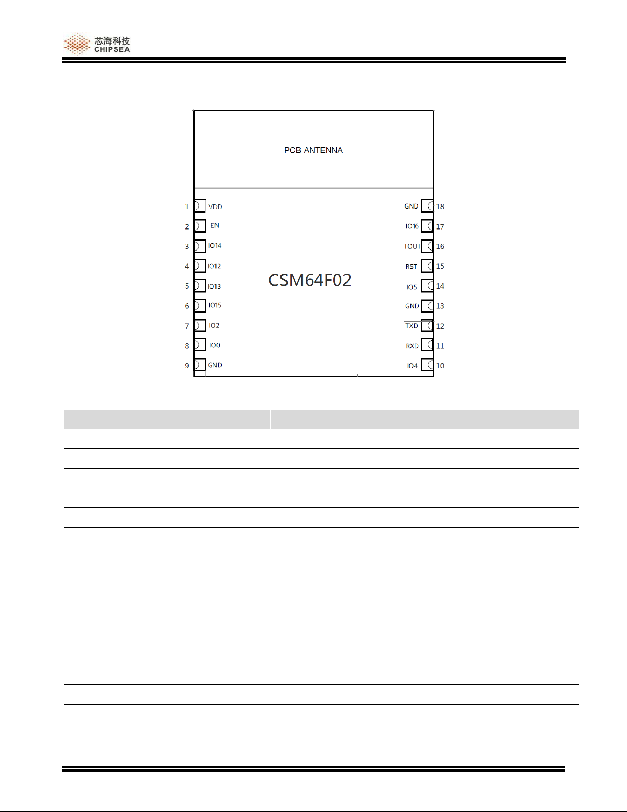
2 Pin Definition
No.
Name
Functions
1
VDD
3.3V power supply. Recommended power capacity is 500mA.
2
EN
Module enable pin; enable at high level
3
IO14
GPIO14; HSPI_CLK
4
IO12
GPIO12; HSPI_MISO
5
IO13
GPIO13; HSPI_MOSI; UART0_CTS
6
IO15
GPIO15; MTDO; HSPICS; UART0_RTS
Pull down from outside
7
IO2
GPIO2; UART1_TXD
Floating (pull up from inside) or pull up from outside
8
IO0
GPIO0
Boot mode selection:
- Pull down: UART downloading;
- Floating or pull up: Boot from Flash
9
GND
Ground
10
IO4
GPIO4
11
RXD
UART0_RXD , GPIO3
CSM64F02 User Manual
Pin Definition
Rev1.2 Page 5 of 13
Page 6

12
TXD
UART0_TXD, GPIO1
13
GND
Ground
14
IO5
GPIO5
15
RST
Reset pin
16
TOUT
ADC port, detect VDD or input voltage of TOUT pin
17
IO16
GPIO16, Can be connected to RST to wake up frome deep sleep
18
GND
Ground
External Connection
Normal Start-up
UART Downloading Mode
GPIO15
Pull down 10K to the ground
Low
Low
GPIO0
Pull up or floating
High
Low
GPIO2
Pull up or floating
High
High
3 Reference Design
3.1 Schematic
CSM64F02 User Manual
Schematic of Peripheral Design
Note: GPIO0 / 2 / 15 also serves as boot mode selection pin and should be paid special attention when being used.
Rev1.2 Page 6 of 13
Page 7

CSM64F02 User Manual
3.2 Placement of Antenna
CSM64F02 module uses 2.4G Wi-Fi MIFA onboard antenna with 2dBi gain. When placing the antenna, please
refer to recommended scheme 1 or scheme 2; the effect of schemes 3, 4 and 5 is bad, so please avoid those schemes
when designing the product.
3.2.1 Recommended Scheme
Scheme 1: Antenna is out of the Board Scheme 2: Antenna is at Board Edges with Keep-
Space
3.2.2 Not Recommended Schemes
Actually measured effects of schemes 3, 4 and 5 are bad. Please do not use those three schemes when
designing product.
Scheme 3: Antenna is at Board Edges Scheme 4: Antenna is in Board Frame
with Cleared Space below with Cleared Space below
Rev1.2 Page 7 of 13
Page 8

Scheme 5: Antenna is Placed in Board Frame with Uncleared Space below
CSM64F02 User Manual
Rev1.2 Page 8 of 13
Page 9

5 Electrical Characteristics
Name
Conditions
Values
Unit
Storage temperature
-40 ~ 85
℃
Max. welding temperature
260
℃
Power supply voltage
IPC/JEDEC J-STD-020
+2.7 ~ +3.6
V
Electrostatic Dsicharge
(HBM)
=25℃
≤2
KV
Electrostatic Dsicharge
(CDM)
=25℃
≤0.5
KV
Name
Symbol
Min. Value
Typical
Value
Max. Value
Unit
Operating temperature
-20
20
+85
℃
Power supply voltage
VDD
2.7
3.3
3.6
V
Name
Min. Value
Typical
Value
Max. Value
Unit
Operating frequency
2412
2484
MHz
Transmitted
power
802.11b @11Mbps
19 dBm
802.11g @54Mbps
14 dBm
802.11n @HT20, MCS7
13 dBm
Receiving
sensitivity
802.11b @11Mbps
-85 dBm
802.11g @54Mbps
-75 dBm
802.11n @HT20, MCS7
-72 dBm
5.1 Absolute Maximum Rationgs
5.2 Recommended Operating Environment
CSM64F02 User Manual
5.3 RF Performance
NOTE: This equipment has been tested and found to comply with the limits for a Class B digital device,
pursuant to part 15 of the FCC Rules. These limits are designed to provide reasonable protection against
harmful interference in a residential installation. This equipment generates, uses and can radiate radio
frequency energy and, if not installed and used in accordance with the instructions, may cause harmful
interference to radio communications. However, there is no guarantee that interference will not occur in a
particular installation. If this equipment does cause harmful interference to radio or television reception,
which can be determined by turning the equipment off and on, the user is encouraged to try to correct
the interference by one or more of the following measures:
—Reorient or relocate the receiving antenna.
—Increase the separation between the equipment and receiver.
Rev1.2 Page 9 of 13
Page 10

CSM64F02 User Manual
Name
Min. Value
Typical
Value
Max. Value
Unit
Transmit 802.11b @11 Mbps
= +17 dBm
170 mA
Transmit 802.11g @54 Mbps
= +15 dBm
140 mA
Transmit 802.11n @MCS7
= +13 dBm
120 mA
Receive 802.11b; package length 1024 bytes, -
80 dBm
50 mA
Receive 802.11g; package length 1024 bytes, -
70 dBm
56 mA
Receive 802.11n; package length 1024 bytes, -
65 dBm
56 mA
Modem-Sleep①
15 mA
Light-Sleep②
0.9 mA
Deep-Sleep③
20 μA
Shut-down
0.5 μA
—Connect the equipment into an outlet on a circuit different from that to which the receiver is
connected.
—Consult the dealer or an experienced radio/TV technician for help.
This device complies with part 15 of the FCC rules. Operation is subject to the following twoconditions:
(1) this device may not cause harmful interference, and
(2) this device must accept any interference received, including interference that may cause undesired
operation.
Changes or modifications to this unit not expressly approved by the party responsible for compliance
could void the user's authority to operate the equipment.
5.4 Power Consumption
Attention:
① Modem-Sleep is used for the application requiring CPU always in operating state such as PWM or I2S
applications etc. When maintaining Wi-Fi connection, it is allowed to turn off Wi-Fi Modem circuit to save
power consumption according to 802.11 standard (such as U-APSD) when there is no data transmission. For
example, in the configuration of DTIM3, it will wake up for 3ms to receive Beacon packet from AP after sleeping
every 300ms, and the averange current is about 15mA.
② Light-Sleep is used for the application with CPU suspendable such as Wi-Fi switch. When maintaining Wi-Fi
connection, it is allowed to turn off Wi-Fi Modem circuit and suspend CPU to save power consumption
according to 802.11 standard (such as U-APSD) when there is no data transmission. For example, in the event
of DTIM3, it will wake up for 3ms to receive Beacon packet from AP after sleeping every 300ms, and the
averange current will be about 9mA.
③ Deep-Sleep is used for the application without the need to always maintain Wi-Fi connection and transmitting
one data packet for a long time such as the sensor measuring temperature every 100s. For example, it will wake
up for 0.3s - 1s every 300s and connect to AP to transmit data, and the averange current may be far smaller than
1mA.
Rev1.2 Page 10 of 13
Page 11

5.5 Ramp up
Indexes
Values
Ramp up rate ( Max to )
≤3℃/s
Preheating
Min. temperature value ( Min)
Typical temperature value ( Typ)
Max. temperature value ( Max)
Time
150℃
175℃
200℃
60 ~ 180s
Ramp up rate ()
≤3℃/s
Above time of duration: temperature ()/ time ()
217℃/ 60~150s
Peak value of temperature ()
Max. temperature value is 260℃ and duration is 10s
Target peak value of temperature ( target value)
260℃ +0/-5℃
Time of duration within actual peak value () 5℃
20~40s
Ramp down rate ( Max to )
≤6℃/s
Time adjusting from 25℃ to peak value of
temperature
Max. 8min.
CSM64F02 User Manual
Rev1.2 Page 11 of 13
Page 12

6 Label and Ordering Information
Model
Description
CSM64F02
Integrating 16M bit Flash
6.1 Label Description
CSM64F02: Part No.
1716: Date Code
MAC: MAC address
QR code: QR code of MAC address
6.2 Ordering Information
CSM64F02 User Manual
Rev1.2 Page 12 of 13
Page 13

7 Packaging Infomation
CSM64F02 User Manual
Packaging Dimension
(Top View)
Rev1.2 Page 13 of 13
Page 14

Host 15B and 15C compliance statement
A host product itself is required to comply with all other applicable FCC equipment
authorization regulations, requirements, and equipment functions that are not
associated with the transmitter module portion. For example, compliance must be
demonstrated: to regulations for other transmitter components within a host product;
to requirements for unintentional radiators (Part 15 Subpart B), such as digital
devices, computer peripherals, radio receivers, etc.; and to additional authorization
requirements for the non-transmitter functions on the transmitter module (i.e.,
Verification or Declaration of Conformity) as appropriate (e.g., Bluetooth and Wi-Fi
transmitter modules may also contain digital logic functions).
The OEM integrator or the host manufacturer is responsible for the overall
compliance of the host products
FCC statement
This device complies with Part 15 of FCC rules. Operation is subject to the following
two conditions: (1) this device may not cause harmful interference and (2) this
device must accept any interference received, including interference that may cause
undesired operation.
RF exposure statement
Human exposure to RF emissions from mobile devices (47 CFR §2.1091) may be
evaluated based on the MPE limits adopted by the FCC for electric and magnetic field
strength and/or power density, as appropriate, since exposures are assumed to
occur at distances of 20 cm or more from persons.
Module statement
The single-modular transmitter is a self-contained, physically delineated, component
for which compliance can be demonstrated independent of the host operating
conditions, and which complies with all eight requirements of § 15.212(a)(1) as
summarized below.
1) The radio elements have the radio frequency circuitry shielded.
2) The module has buffered modulation/data inputs to ensure that the device will
comply with Part 15 requirements with any type of input signal.
3) The module contains power supply regulation on the module.
4) The module contains a permanently attached antenna.
5) The module demonstrates compliance in a stand-alone configuration.
6) The module is labeled with its permanently affixed FCC ID label
7) The module complies with all specific rules applicable to the transmitter, including
all the conditions provided in the integration instructions by the grantee.
8) The module complies with RF exposure requirements.
Page 15

Changes or modifications to this unit not expressly approved by the party responsible for compliance
could void the user's authority to operate the equipment.
FCC statement
The final host device, into which this RF Module isintegrated" hasto be labelled with an
auxilliary lable stating the FCC IDofthe RF Module,such as"
"Contains FCC ID:2AGM5CSM64F02"
This devic e is acting as slave and operat ing in the 2.4 GHz (2412 ~2462 MHz)
band.
Ad Hoc function is supported but not able to operate on non-US frequencies.
Do not use the device with the environment which below minimum -10 ℃ or maximum
over 50℃ .
NOTE: This equipment has been tested and found to comply with the limits for
a Class B digital device, pursuant to part 15 of the FCC Rules. These limits are
designed to provide reasonable protection against harmful interference in a
residential installation. This equipment generates uses and can radiate radio
frequency energy and, if not installed and used in accordance with the
instructions, may cause harmful interference to radio communications.
However, there is no guarantee that interference will not occur in a particular
installation. If this equipment does cause harmful interference to radio or
television reception, which can be determined by turning the equipment off and
on, the user is encouraged to try to correct the interference by one or more of
the following measures:
- Reorient or relocate the receiving antenna.
- Increase the separation between the equipment and receiver.
-Connect the equipment into an outlet on a circuit different from that to which
the receiver is connected.
-Consult the dealer or an experienced radio/TV technician for help
This transmitter/module must not be collocated or operating in conjunction
with any other antenna or transmitter except in accordance with the FCC multi-transmitter
product procedures.
 Loading...