


Novel Low Cost Green-Power PWM Controller
Feature
Low Cost, PWM&PFM&CRM (Cycle
Reset Mode)
Low Start-up Current (about 1.5µA)
Low Operating Current (about 1.4mA)
Current Mode Operation
Under Voltage Lockout (UVLO)
Built-in Synchronized Slope
Compensation
Built-in Low EMI Technique
Programmable PWM Frequency
Audio Noise Free Operation
Leading edge Blanking on Sense input
Constant output power limiting for
universal AC input Range
SOT-23-6L 、SOP8 and DIP-8 Pb-Free
Applications
Switching AC/DC Adaptor
Battery Charger
Open Frame Switching Power Supply
General Description
The CR6853 is a highly integrated low cost
current mode PWM controller, which is ideal
for small power current mode of offline
AC-DC fly-back converter applications.
Making use of external resistors, the IC
changes the operating frequency and
automatically enters the PFM/CRM (Cycle
Reset Mode) under light-load/zero-load
conditions. This can minimize standby
power consumption and achieve powersaving functions. With a very low start-up
current, the CR6853 could use a large value
start-up resistor (2MΩ).
Built-in synchronized slope compensation
enhances the stability of the system and
avoids sub-harmonic oscillation. Dynamic
peak current limiting circuit minimizes output
power change caused by delay time of the
system over a universal AC input range.
Leading edge blanking circuit on current
CR6853
With Low EMI Technique
Packaging
Compatible with SG6848 (6849) /
SG5701/SG5848/LD7535 (7550) /
OB2262 (2263)/OB2278((((2279))))
Complete Protection with
Soft Clamped GATE output voltage
18.0V
VDD over voltage protect 34.0V
Cycle-by-cycle current limiting
Sense Fault Protection
OTP (Over Temperature Protection)
Output SCP (Short circuit Protection)
Output OLP (Over Load Protection)
Latch mode After OLP&SCP
High-Voltage CMOS Process with ESD
Standby Power Supplies
Set-Top Box Power Supplies
384X Replacement
sense input could remove the signal glitch
due to snubber circuit diode reverse
recovery and thus greatly reduces the
external component count and system cost
in the design. Cycle-by-Cycle current
limiting ensures safe operation even during
short-circuit.
Excellent EMI performance is achieved
built-in soft driver and low EMI technique.
The CR6853 offers perfect protection like
OVP(Over Voltage Protection)、OLP(Over
Load Protection) 、 SCP(Short circuit
protection)、OTP、Sense Fault Protection
and OCP(Over current protection). The
CR6853’s output driver is soft clamped to
maximum 18.0V to protect the power
MOSFET. CR6853 is offered in SOT-23-6L,
SOT-8 and DIP-8 packages.
Dec, 2007 V1.1 1/11
Chengdu Chip-Rail Tech. Co., Ltd. http://www.chiprail.com
CR6853
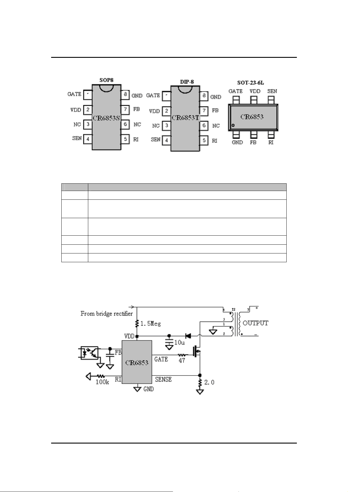
Pin Assignment
Pin Descriptions
Name Description
GND GND Pin
Voltage feedback pin. Output current of this pin could controls the PWM
FB
duty cycle、OLP and SCP.
RI
SEN
VDD
GATE
This pin is to program the switching frequency. By connecting a resistor
to ground to set the switching frequency.
Current sense pin, a resistor connects to sense the MOSFET current.
Supply voltage pin.
Totem output to drive the external power MOSFET.
TYPICAL APPLICATION
Dec, 2007 V1.1 2/11
Chengdu Chip-Rail Tech. Co., Ltd. http://www.chiprail.com
8 (10S)
CR6853
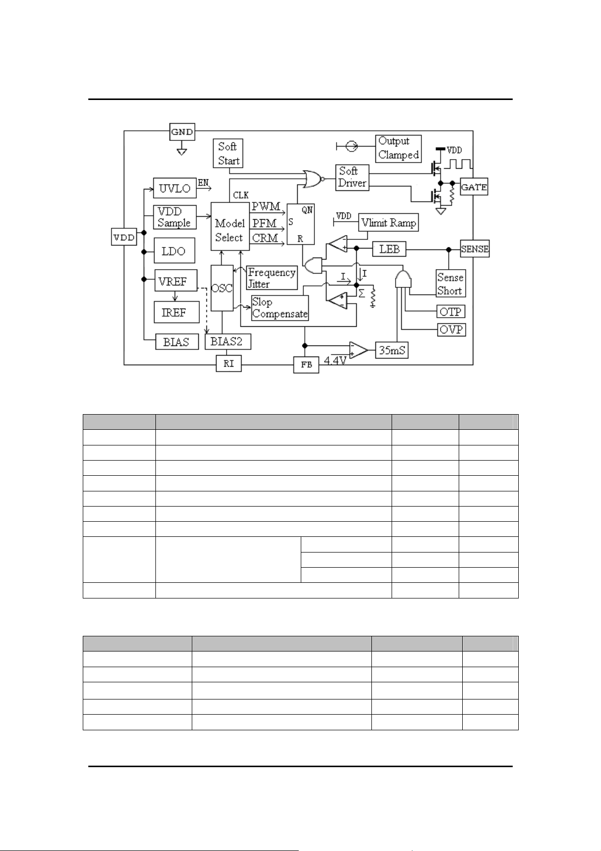
Block Diagram
Simplified Internal Circuit Architecture
Absolute Maximum Ratings
Symbol Parameter Rating Unit
V
DD
I
OVP
V
FB
V
SEN
P
D
T
L
T
STG
Supply voltage Pin Voltage 40 V
VDD OVP maximal enter current 20 mA
Input Voltage to FB Pin -0.3 to 6V V
Input Voltage to SEN Pin -0.3 to 6V V
Power Dissipation 300 mW
ESD Capability, HBM Model 2500 V
ESD Capability, Machine Model 250 V
Lead Temperature
(Soldering)
Storage Temperature Range -55 to + 150
SOT-23-6L (20S)
DIPSOP-8 (10S)
220
260
230
℃
℃
℃
℃
RECOMMENDED OPERATION CONDITION
Symbol Parameter Min ~ Max Unit
VDD VDD Supply Voltage 10~30 V
RI RI PIN Resistor Value 100 K ohm
TOA Operation Ambient Temperature -20~85
P
Maximal Output Power 0~80 W
OMAX
F
PWM
Frequency of PWM 30~150 kHz
℃
Dec, 2007 V1.1 3/11
Chengdu Chip-Rail Tech. Co., Ltd. http://www.chiprail.com
CR6853
Electrical Characteristics
Symbol
Supply Voltage (VDD Pin)
VDD
VDD
VDD
I
ST
I
SS
ON
OFF
CLAMP
Startup Current 3.0 20.0
Operating Current
Turn-on Threshold Voltage 13.0 14.0 15.0 V
Turn-off Threshold Voltage 7.8 8.8 9.8 V
VDD Clamp Voltage I
Anti Intermission Surge
VDD
AIS
VDD Voltage
T
OFF
T
RESTART
Over temperature Protection 130
Temperature restart 100
Parameter Conditions Min. Typ. Max. Unit
(Ta=25°C unless otherwise noted, VDD = 15V)
VFB=0V 3.0
VFB=3V 1.4
VFB=Open 1.0
=10mA 34.0
VDD
12.7
µA
mA
mA
mA
V
V
℃
℃
Voltage Feedback (FB Pin)
IFB Short Circuit Current VFB=0V 1.2
VFB Open Loop Voltage VFB=Open 4.8
I
Zero Duty Cycle FB current 1.47
FB_0D
I
PFM
I
CRM
V
PFM
V
CRM
I
OLP&SCP
V
OLP&SCP
T
OLP&SCP
Enter PFM FB current 1.37
Enter CRM FB current 1.45
Enter PFM Threshold V
FB
0.51
Enter CRM Threshold VFB 0.30
Enter OLP&SCP FB current 152
Enter OLP&SCP FB voltage 3.7
OLP&SCP min. delay Time RI=100K 33 35 50 mS
Current Sensing (SEN Pin)
SEN Minimum Voltage Level RI=100K,
V
TH_L
0.70
FB=3.3V
mA
V
mA
mA
mA
V
V
uA
V
V
V
TH_H
0.80
V
FB=3.3V
TPD Delay to Output FB=3.3V 75 ns
SEN Maximum Voltage Level RI=100K,
RCS Input Impedance
V
SCP
Dec, 2007 V1.1 4/11
Sense short protect voltage 177
40 KΩ
mV
Chengdu Chip-Rail Tech. Co., Ltd. http://www.chiprail.com
 Loading...