

Page 1
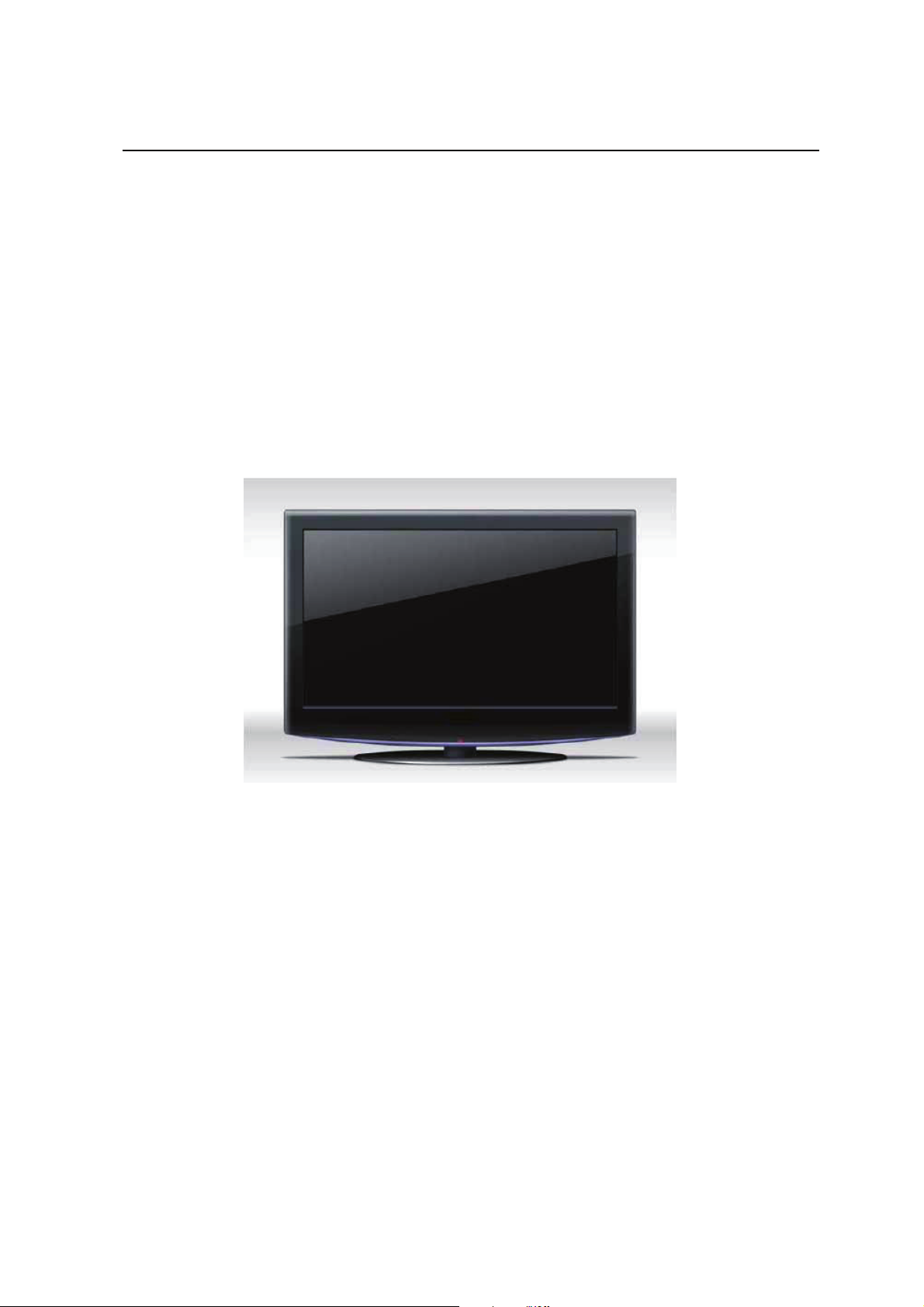
SERVICE MANUAL
Order No.: TV0904S003V0
COLOR TV
Model No. : HBTV-3201HD
CHASSIS: Mstar 6U89
WARNING
This service information is designed for experienced repair technicians only and is not designed for use by the general public. It does
not contain warnings or cautions to advise non-technical individuals of potential dangers in attempting to service a product. Products
powered b electricity should be serviced or repaired only by experienced professional technicians. Any attempt to service or repair the
product deal with in this service information by anyone else could result in serious injury or death.
1
Page 2

CONTENTS
Table of contents………………..................…………………………….2
1. General Information
1-1. General Guidelines...…………………………………………………..4
1-2. Important notice………………………………………………………...4
1-3. How to read this Service Manual……………………………………..5
…………...............…………………………..4
2. Specifications……………………………………………....................6
3. Location of Controls and Components
3-1.Board Location……………………………………………………………..7
3-1-1. L32R1 Board Location ……………………………………………………..7
3-2. Main Board……………………………………………………………7
3-2-1. Function Description……………………………………………………..8
3-2-2. Connector definition……………………………………………………..8
3-3. Power Board……………………………………………………………9
...........................7
3-3-1. Connector definition……………………………………………………9
3-3-2. Function Description……………………………………………………9
3-4. LCD Panel…………………………………………… …………… ……10
3-4-1. Connector definition……………………………………………………10
3-4-2. Function Description……………………………………………………11
4. Disassemble and Assemble
4-1 L32R1………………………………………………………………….…11
4-1-1 Remove the Pedestal………………………………………………….…12
4-1-2 Remove the Back Cover……………………………………………….…12
4-1-3 Remove the Main board……………………………………………….…12
4-1-4 Remove the power module…………………………………………….…12
4-1-5 Remove the speaker………………………………………………….…13
4-1-6 Remove the remote control……………………………………………. 13
…………………...........………….11
4-1-7 Remove the Keypad Assembly……………………………………….… 13
5. Installation Instructions ………..................………………..…..14
2
Page 3

6. Operation Instructions
…………………………........................19
6-1 Front Panel Controls …………………………………………….........19
6-2 Rear Panel Controls ……………...……………………………..........19
6-3 Setting up your Remote Controller....................................................20
7. Electrical Parts
............................................................................20
7-1. Circuit diagram ...............................................................................20
7-2 .Wiring Connection Diagram...........................................................31
8. Measurements and Adjustments
.......................................31
8-1. Service Mode ..................................................................................31
8-1-1.How to enter into Service Mode
8-1-2.How to exit…
8-1-3. The default of Factory Mode Menu
.....................................................................................31
............................................................31
...............................................31
9. Trouble Shooting
9-1. Simple check ...............................................................................32
......................................................................32
9-2. Main board failure check ..............................................33
9-3. Pannel failure ...............................................................................34
3
Page 4

1. General Information
1-1 General Guidelines
When servicing, observe the original lead dress. If a short circuit is found, replace all parts which
have been overheated or damaged by the short circuit.
After servicing, see to it that all the protective devices such as insulation barriers, insulation papers
shields are properly installed.
After servicing, make the following leakage current checks to prevent the customer from being
exposed to shock hazards.
1) Leakage Current Cold Check
2) Leakage Current Hot Check
3)Prevention of Electro Static Discharge(ESD)to Electrostatically Sensitive
1-2 Important notice
1-2-1. Follow the regulations and warnings
Most important thing is to list up the potential hazard or risk for the service personnel to open the
units and disassemble the units. For example, we need to describe properly how to avoid the
possibility to get electrical shock from the live power supply or charged electrical parts (even the
power is off).
This symbol indicates that high voltage is present inside. It is dangerous to
make any king of contact with any inside part of this product.
This symbol indicates that there are important operating and maintenance
instructions in the literture accompanying the appliance
1-2-2. Be careful to the electrical shock
To prevent damage which might result in electric shock or fire, do not expose this TV set to rain or
excessive moisture. This TV must not be exposed to dripping or splashing water, and objects
Filled with liquid, such as vases, must not be place on top of or above the TV
1-2-3. Electro static discharge (ESD)
Some semiconductor (solid state) devices can be damaged easily by static electricity. Such
Components commonly are called Electrostatically Sensitive (ES) Devices. The following
tech-niquesshouldbeusedtohelpreducetheincidenceofcomponentdamagecausedbyelectro
Static discharge (ESD).
1-2-4. About lead free solder (PbF)
This product is manufactured using lead-free solder as a part of a movement within the consum-er
products industry at large to be environmentally responsible. Lead-free solder must be used in the
servicing and repair of this product.
1-2-5. Use the genewing parts (specified parts)
Special parts which have purposes of fire retardant (resistors),high-quality sound (capacitors), low
noise(resistors), etc. are used.
When replacing any of components, be sure to use only manufacture's specified parts shown in
the parts list.
Safety Component
● Components identified by mark have special characteristics important for safety.
4
Page 5
1-2-6. Safety Check after Repairment
Confirm that the screws ,parts and wiring which were removed in order to service are put in the
original positions, or whether there are the portions which are deteriorated around the serviced
places serviced or not. Check the insulation between the antenna terminal or external metal and
the AC cord plug blades. And be sure the safety of that.
Insuration Test
1. Unplug the plug from the AC outlet.
2. Remove the antenna terminal on TV and turn on the TV.
3. Insulation resistance between the cord plug terminals and the eternal exposure metal
should be more than M ohm by using the 500V insulation resistance meter
4. If the insulation resistance is less than M ohm, the inspection repair should be required.
If you have not the 500V insulation resistance meter, use a Tester.
External exposure metal: Antenna terminal Headphone jack
1-2-7. Ordering Spare Parts
Please include the following informations when you order parts. (Particularly the Version
letter)
1. Model number and Version letter
The model number can be found on the back of each product and the Version letter can
be found at the end of the serial number.
2. Part No. and Description
You can find them in your service manual.
1-2-8. Photo used in this manual
The illustration and photos used in this Manual may not base on the final design of products, which
may differ from your products in some way.
1-3. How to read this Service Manual
1-3-1. Using Icons
Icons are used to attract the attention of the reader to specific information. The meaning of each icon is
described in the table below:
Note:
A “note” provides information that is not indispensable, but may nevertheless be valuable to the
reader, such as tips and tricks.
Caution:
A “caution” is used when there is danger that the reader, through incorrect manipulation,
may damage equipment, loose data, get an unexpected result or has to restart(part of)
a procedure.
Warning:
A “warning” is used when there is danger of personal injury.
5
Page 6
Reference:
A “reference” guides the reader to other places in this binder or in this manual, where
he/she will find additional information on a specific topic.
2. Specifications
10.2KG(withstand)
796*233*582
(with stand
870*267*657
6
Page 7
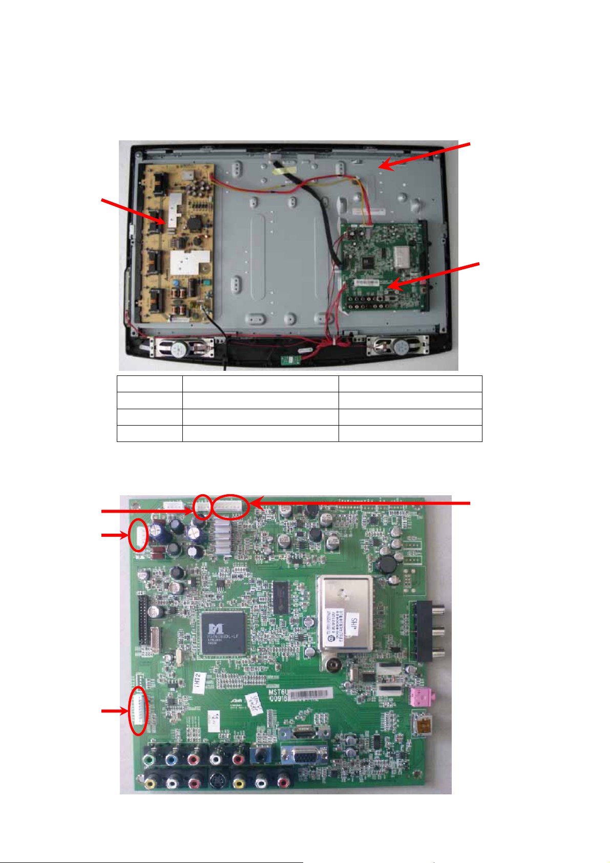
3. Location of Controls and Components
3-1 Board Location
3-1-1
B
L32H8 Board Location
A
C
No. Parts number Description
A Board 0094001236DA LCD PANEL
B Board 0094001274A Power Supply
C Board DZ0UQ0E0102M Mainboard Assembly
3-2 Main Board
CON2
CON17
CN5
CON28
7
Page 8
3-2-1 Function Description:
Main Board:
Process signal which incept from exterior equipment,then translate into signal that panel can
display.
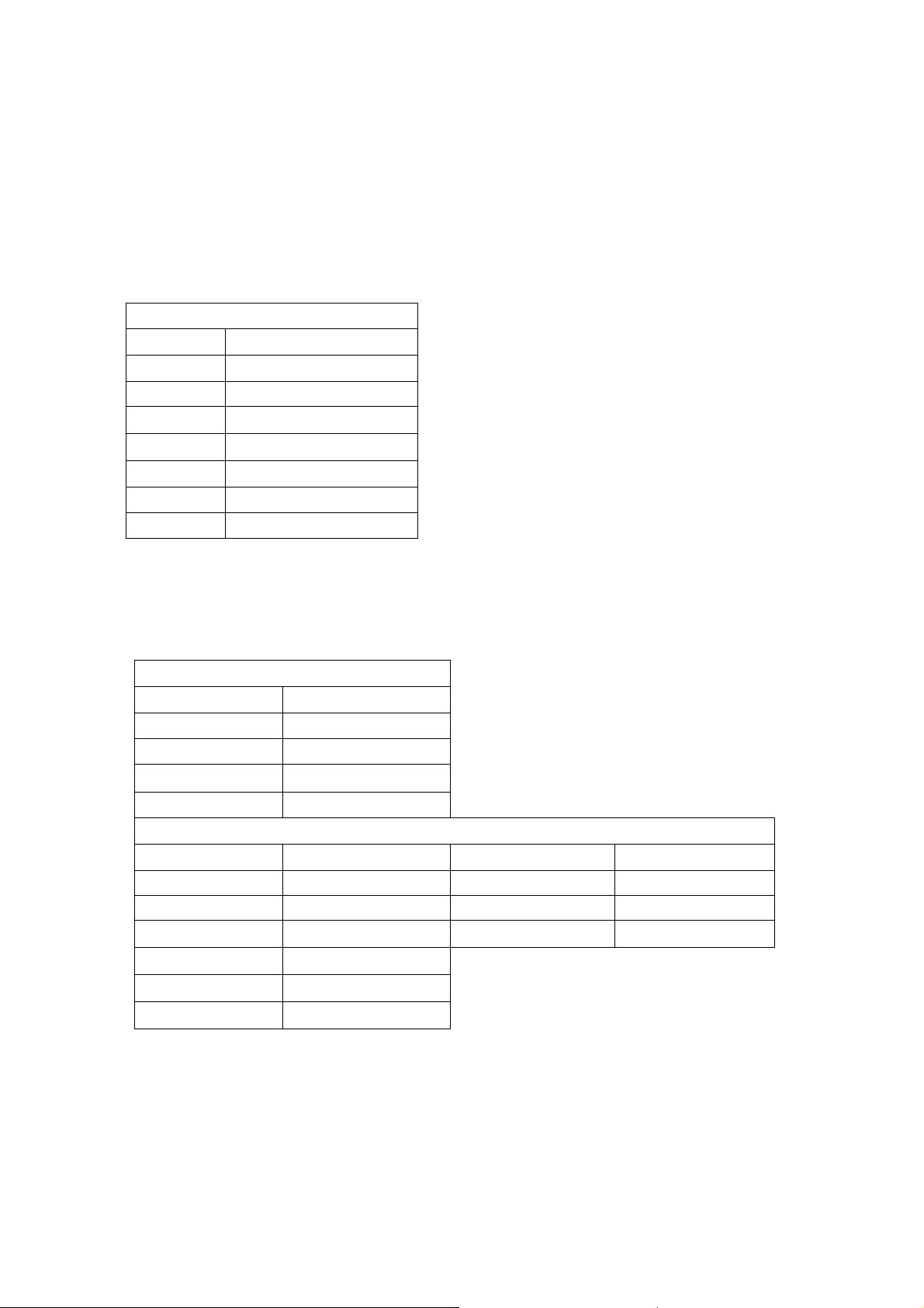
3-2-2 Connector definition
Main board connector
Power connectors (CON28)
CON28
Pin number Signal name
1 STN
2 GND
3 5VSTB
4 GND
5 GND
6 12VA
7 12VA
Notes:
CON28-Pin6.7 :The power for the mainboard when system power on.
CON28-Pin3 :The power for the mainboard when system standby.
CON28-Pin1 : System power on/standby, System board will use this pin to control system power.
Control connectors (CON2,CN5)
CON2
Pin number Signal name
1 ADJ
2 ON/OFF
3 GND
4 5V
Pin number Signal name Pin number Signal name
1 5VSTB 7 GND
2 GND 8 KEY1
3 LED-B 9 KEY2
4 LED-R
5 5VSTB
6 IRIN
Notes:
CON2-Pin3,4 : N/A
CON2-Pin2 : The control pin for the backlight.
CON2-Pin1 : The adjust pin for the backlight.
CN5-Pin6 : The pin for the remote.
CN5-Pin8,9 : The pin for the key.
Signal connectors (CON17)
CN5
8
Page 9
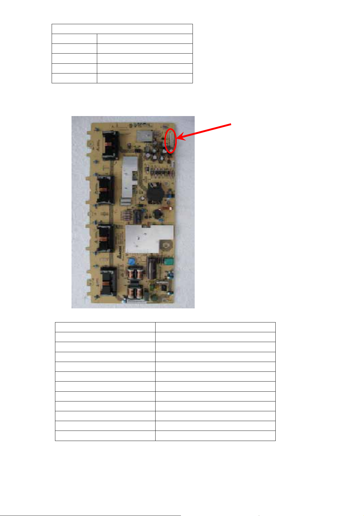
CON17
Pin number Signal name
1 L +
2 L -
3 R -
4 R +
3-3. Power Board
3-3-1 Connector definition
CN2
CN2
PIN NUMBER DESIGNATION
1 12V
2 12V
3 GND
4 GND
5 5VSTB
6 GND
7 STN
8 SEL
9 V-IPWM
10 BL-ON
11 V-EPWM
3-3-2 Function Description:
Supply power for Main board and Panel
9
Page 10
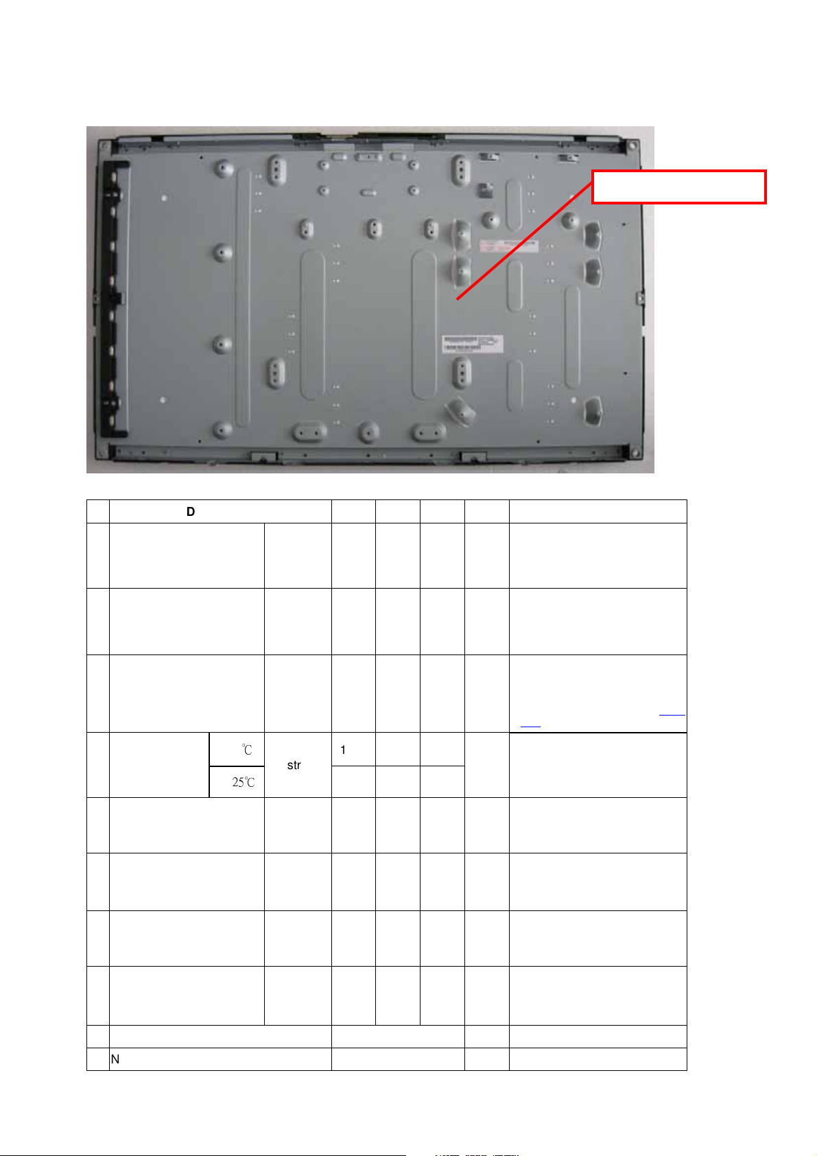
3-4. LCD Panel
ensure
3-4-1 Connector definition
BACKLIGHT CONNECTOR PIN CONFIGURATION :
Description Min Typ Max Unit
1 Operating Voltage Vo 639 710 781 Vrms
2 Operating Current Io 12 12.5 13 mArms
3 BL Total Power Dissipation PBL 76
78
80 Watt
AU(T315XW02 VP)
Condition/Note
1. Dimming range is set 100%
2. Base on lamp specification, for each
lamp need to be applied at least
minimum operating voltage to ensure
each lamp can be normally worked!
1. Dimming range is set 100%
2. Base on lamp specification, for each
lamp need to be applied at least
minimum operating current to ensure
each lamp can be normally worked!
1. Dimming range is set 100%.
2. In order to get typical light out, the
backlight need to be applied typical
power.
3. Input power of JIG BD is about 78 W
(typ) by AUO measure!
At 0
℃
4 Striking Voltage
At
25℃
Vstrike
5 Striking Time Ts 1000
1500 1650
1350 1500
- 1500 msec
Vrms
6 Operating Frequency fo kHz
PWM Operating Frequency F_PWM 120 180 240 Hz
7
PWM Dimming Duty Ratio D_PWM
8
20
9 Lamp Type U type
100
-
%
10 Number of Lamps 4 pcs
10
1. Base on lamp specification, to
each lamp can be normally ignited,
need to apply at least minimum
striking voltage to each lamp
1. To ensure each lamp can be normally
ignited, each lamp need to be applied
at least minimum striking voltage
during minimum striking time.
1. Operating frequency is set by
customer.
2. Need to double confirm display
quality.(*)
1. PWM frequency is set by customer.
2. Need to double confirm display
quality.(*)
Note 1. Dimming range
Note 2.
Note 3. Duty ratio definition.
Page 11
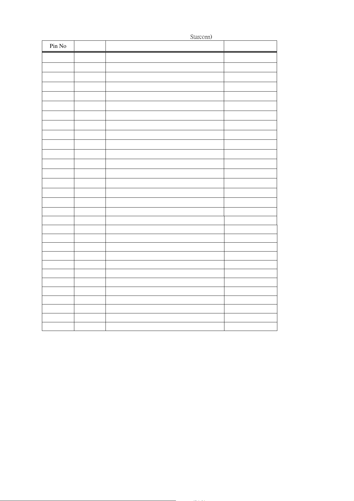
LVDS:
Connector on Panel: 093G30-B0001A-1 (Manufactured by
Pin No Symbol Description Default
1 VCC +12V, DC, Regulated
2 VCC +12V, DC, Regulated
3 VCC +12V, DC, Regulated
4 VCC +12V, DC, Regulated
5 GND Ground and Signal Return
6 GND Ground and Signal Return
7 GND Ground and Signal Return
8 GND Ground and Signal Return
9 LVDS Option Low/Open for Normal (NS), High for JEIDA NS mode
10 Reserved Open AUO internal test
11 GND Ground and Signal Return for LVDS
12 RIN0- LVDS Channel 0 negative
13 RIN0+ LVDS Channel 0 positive
14 GND Ground and Signal Return for LVDS
15 RIN1- LVDS Channel 1 negative
16 RIN1+ LVDS Channel 1 positive
17 GND Ground and Signal Return for LVDS
18 RIN2- LVDS Channel 2 negative
19 RIN2+ LVDS Channel 2 positive
20 GND Ground and Signal Return for LVDS
21 RCLK- LVDS Clock negative
22 RCLK+ LVDS Clock positive
23 GND Ground and Signal Return for LVDS
24 RIN3- LVDS Channel 3 negative
25 RIN3+ LVDS Channel 3 positive
26 GND Ground and Signal Return for LVDS
27 Reserved Open or High AUO internal test
28 Reserved Open or High AUO internal test
29 GND Ground and Signal Return
30 GND Ground and Signal Return
Starconn
)
3-4-2 Function Description:
Display the signal.
4. Disassemble and assemble
4-1. L32R1
11
Page 12
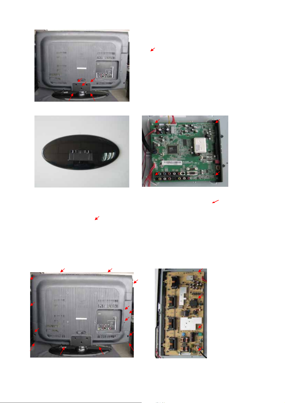
4-1-1 Remove the Pedestal
① Lay down the unit so that rear
① Remove the fourteen screws
② Then remove the back cover from
4-1-3 Remove the Main board
① Remove the four screws indicated
cover faces upward
② Remove the five screws from the rear
② Disconnected the coupler CON28、
cover indicated with
③ Then remove the pedestal
③ Remove the Main board
indicated on figure above by
the unit.
on the figure above by
CON2、CON17、CN5
4-1-2 Remove the Back Cover
4-1-4 Remove the power module
12
Page 13
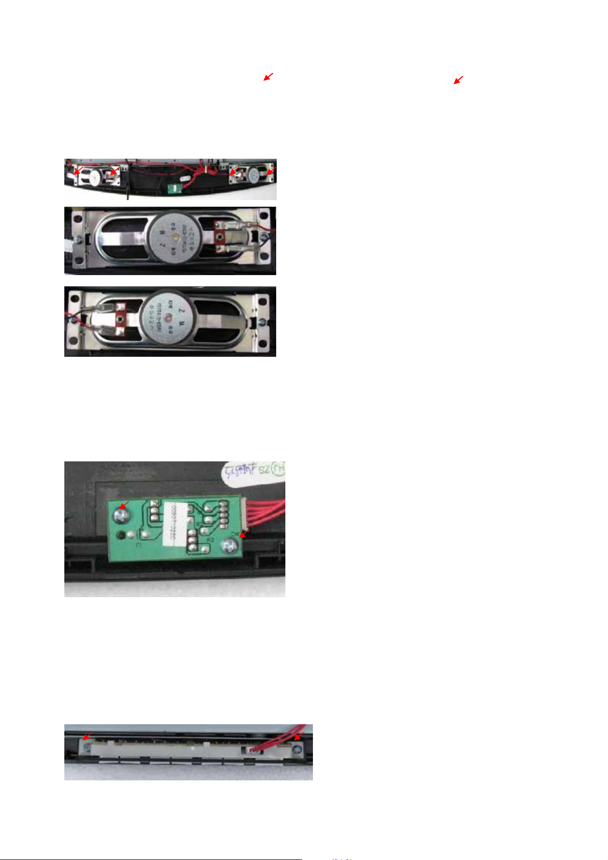
① Remove the four screws
indicated on the figure above by
② Then remove the power module
4-1-5 Remove the speaker
Remove the four screws,
then take out the speaker
① Remove the two screws indicated on
the figure above by
② Disconnected the coupler CN1
③ Remove the Keypad Assembly
4-1-6 Remove the remote control
Remove the two screws,
then take out the remote control board.
4-1-7 Remove the Keypad Assembly
13
Page 14
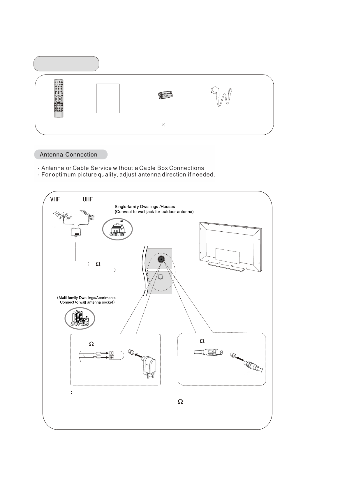
5. Installation Instructions
Accessories
Accessories
STILL
MUTE
DISPLAY
SLEEP PIP
SCAN
ABC@
DEF
GHI$
MNO
JKL%
STUVPQR& WXYZ
*#()
TV/AV
SWAP
P.STD S.STD
CH+
VOL-
MENU
VOL+
CH-
H.LOCK
TIMER ZOOM
CH.LIST EXIT
Remote controller
outdoor
antenna
(not supply)
User's manual
Antenna input
75 standard
coaxial type
Alkaline battery
(AA) 2
ANT IN
Power cable
300 twin-lead cable
75 coaxial cable
Note
* It is recommended that you'd better use 75
disturbance caused by airwave.
Antenna adapter
(not supply)
* Don't bind antenna cable and electric wire together.
Plug
(additional purchase)
coaxial cable to remove the
14
Page 15
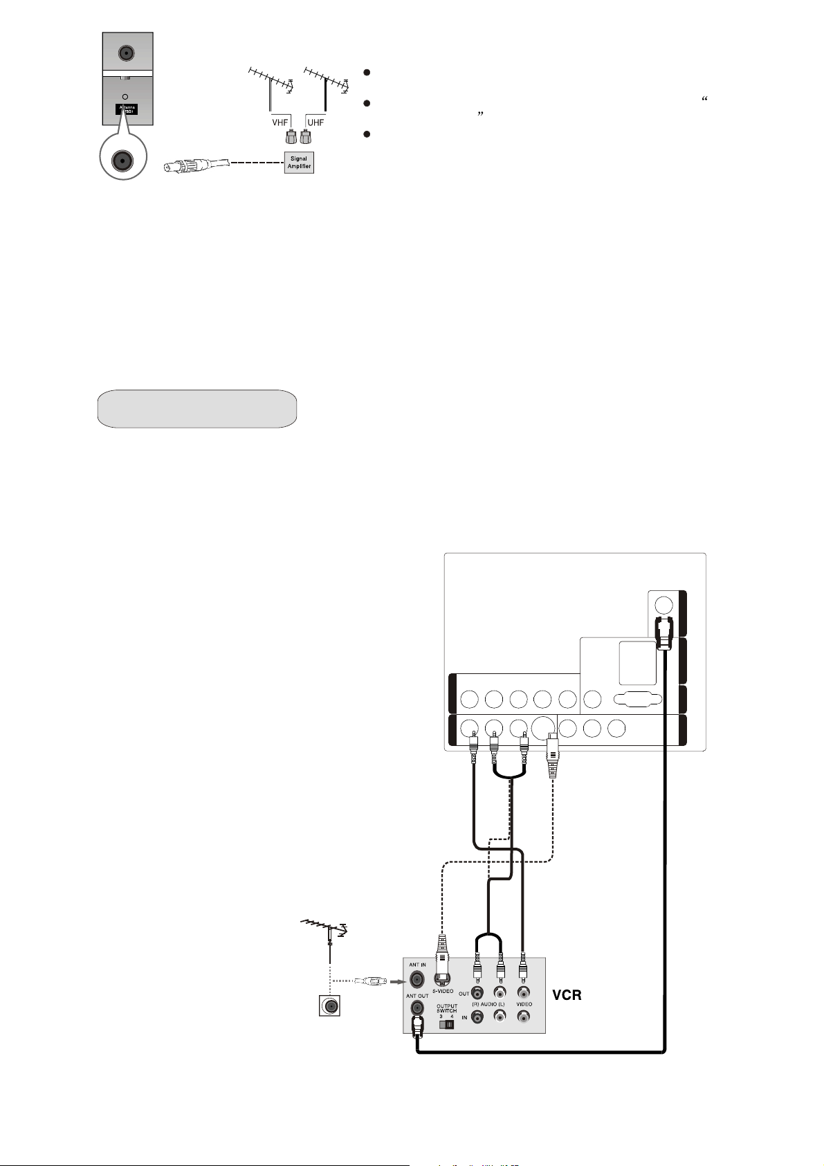
To improve picture quality in a poor signal area, purchase
and install a signal amplifier.
If the antenna needs to be split for two Tv`s, install a 2-
WaySignal Splitter in the connections.
If the antenna is not installed properly, contact your dealer
for assistance.
NOTE: All cables shown are not included with the TV.
Choose Your Connection
There are several ways to connect your television, depending on the components you
want to connect and the quality of the signal you want to achieve. The following are
examples of some ways to connect your TV.
Choose the connection which is best for you.
VCR Connection
- To avoid picture noise (interference), leave an adequate distance between the VCR and TV.
Connection Option 1
Set VCR output switch to channel 3 or 4 and
then tune the TV to the same channel number.
Connection Option 2
1. Connect the audio and video cables from the
VCR's output jacks to the TV input jacks, as
shown in the figure.
When connecting the TV to VCR, match the
jack colors (Video = yellow, Audio Left = white,
and Audio Right = red).
If you connect an S-VIDEO output from VCR to
the S-VIDEO input, the picture quality is
improved; compared to connecting a regular
VCR to the Video input.
2. Insert a video tape into the VCR and press
PLAY on the VCR. (Refer to the VCR owner`s
manual.)
Y Pb/Cb Pr/Cr L-AUDIO-R
CONMPENT IN
Av1 IN
VIDEO1 L-AUDIO-R S-VIDEO VIDEO L-AUDIO-R
L R
VGA/DTV
AUDIO
VGA
AV OUT VGA IN HDMI2 IN ANT IN
3. Select the input source with using the
TV/AV button on the remote control, and
then press CH+/- button to select the source,
press the VOL+ button to confirm.
15
Page 16
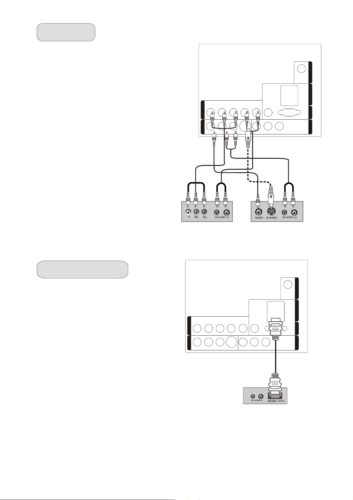
DVD Setup
How to connect
1. Connect the DVD video outputs (Y, Pb/Cb,
Pr/Cr) to the COMPONENT (Y, Pb/Cb, Pr/Cr)
input jacks on the TV and connect the DVD
audio outputs to the AUDIO jacks on the TV,
as shown in the figure.
2. If your DVD only has an S-Video output
jack, connect this to the S-VIDEO input
on the TV and Connect the DVD audio
outputs to the AV IN jacks on the TV,
as shown in the figure.
NOTE: If your DVD player does not have
component video output, use S-Video.
How to use
1. Turn on the DVD player, insert a DVD.
2. Use the TV/AV button on the remote
control to select S-VIDEO or YPbPr/YCbCr
mode.
3. Press Play button on external equipment
for program play.
4. Refer to the DVD player's manual for
operating instructions.
Y Pb/Cb Pr/Cr L-AUDIO-R
CONMPENT IN
Av1 IN
VIDEO1 L-AUDIO-R S-VIDEO VIDEO L-AUDIO-R
VGA/DTV
AUDIO
or
DVD
VGA
AV OUT VGA IN HDMI2 IN ANT IN
HDMI or DVI Setup
-To watch digitally broadcast programs,
purchase and connect a digital set-top
box.
How to connect
Use the TV`s COMPONENT (Y, Pb/Cb,
Pr/Cr) IN jacks, VGA or HDMI port for
video connections, depending on your
set-top box connections available.
Y Pb/Cb Pr/Cr L-AUDIO-R
CONMPENT IN
Av1 IN
VIDEO1 L-AUDIO-R S-VIDEO VIDEO L-AUDIO-R
Then, make the corresponding audio
connections.
How to use
1. Turn on the digital set-top box.
(Refer to the owner`s manual for the digital set-top box.)
2. Use TV/AV on the remote control to select PC or HDMI
(Y, Pb/Cb, Pr/Cr) mode.
3. Press Play button on external equipment for program play.
VGA/DTV
AUDIO
VGA
AV OUT VGA IN HDMI2 IN ANT IN
16
Page 17
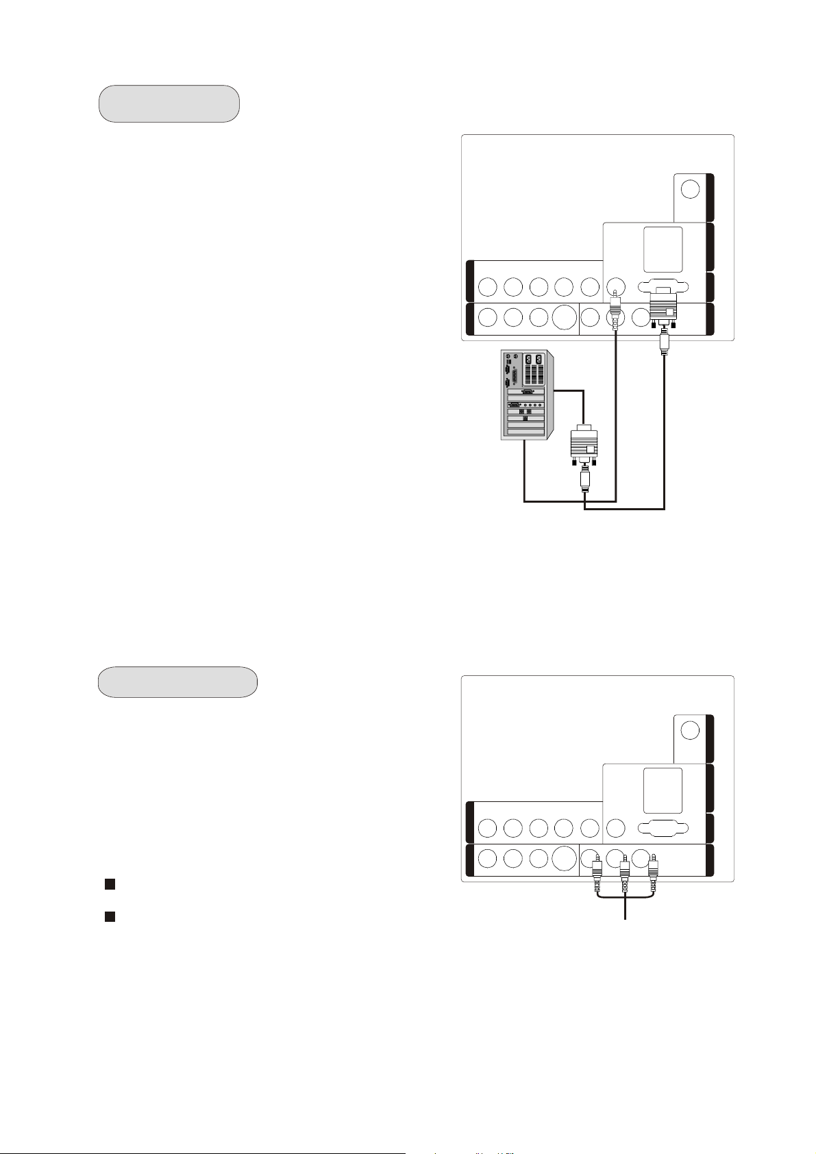
PC Setup
How to connect
1. Use the TV`s PC IN port for video connections.
2. Then, make the corresponding audio
connection. If using a sound card, adjust the
PC sound as required.
How to use
1. Turn on the PC and the TV.
2. Turn on the display by pressing the POWER
button on the TV's remote control.
3. Use TV/AV on the remote control to select
PC source.
4. Check the image on your TV. There may be
noise associated with the resolution, vertical
pattern, contrast or brightness in PC mode.
If noise is present, change the PC mode to
another resolution, change the refresh rate to
another rate or adjust the brightness and contrast
on the menu until the picture is clear. If the refresh
rate of the PC graphic card can not be changed,
change the PC graphic card or consult the manufacturer
of the PC graphic card.
CONMPENT IN
Av1 IN
VIDEO1 L-AUDIO-R S-VIDEO VIDEO L-AUDIO-R
Y Pb/Cb Pr/Cr L-AUDIO-R
VGA/DTV
AUDIO
VGA
AV OUT VGA IN HDMI2 IN ANT IN
NOTES:
1 Avoid keeping a fixed image on the TV's screen for a long period of Time. The fixed image
may become permanently imprinted on the screen.
2 The synchronization input form for Horizontal and Vertical frequencies is separate.
3 To obtain the best picture, do not play the USB, YPbPr, HDMI or VGA source at the same
time.
Monitor Out Setup
The TV has a special signal output capability
which allows you to hook up a second TV or
monitor.
Connect the second TV or monitor to the TV`s
AV OUT. See the Operating Manual of the second
TV or monitor for further details regarding that
device`s input settings.
Notes:
Y Pb/Cb Pr/Cr L-AUDIO-R
CONMPENT IN
Av1 IN
VIDEO1 L-AUDIO-R S-VIDEO VIDEO L-AUDIO-R
VGA/DTV
AUDIO
VGA
YPbPr, PC, HDMI, S-Video input sources
cannot be used for Monitor out.
When connecting with external audio
equipments, such as amplifers or speakers,
please turn the TV speakers off.
AV OUT VGA IN HDMI2 IN ANT IN
17
Page 18
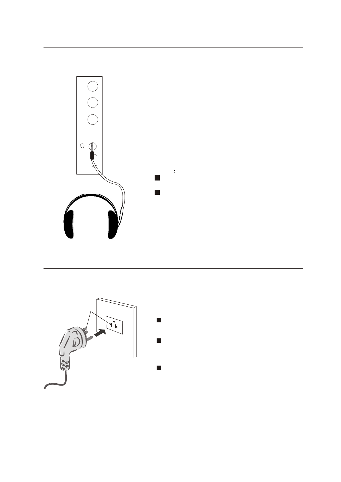
Connecting Headphones
You can connect a set of headphones to your set if you wish to watch a
TV programme without disturbing the other people in the room.
Plug a set of headphones into the 3.5mm
L - AUDIO -RVIDEO 2HDMI 1
mini-jack socket on the rear panel of the set.
Note
Prolonged use of headphones at a high volume
may damage your hearing.
You will not receive sound from the speakers
when you connect headphones to the system.
Power source
Wider Hole
and Blade
Polarized AC Cord Plug
AC Outlet
TO USE AC POWER SOURCE
Use the AC polarized line cord provided for
operation on AC. Insert the AC cord plug into
a standard polarized AC outlet.
NOTES:
Never connect the AC line cord plug to other
than the specified voltage. Use the attached power
cord only.
If the polarized AC cord does not fit into a nonpolarized AC outlet, do not attempt to file or cut
the blade. It is the user`s responsibility to have
an electrician replace the obsolete outlet.
If you cause a static discharge when touching
the unit and the unit fails to function, simply
unplug the unit from the AC outlet and plug it
back in. The unit should return to normal operation.
Polarized AC Cord Plug.
18
Page 19
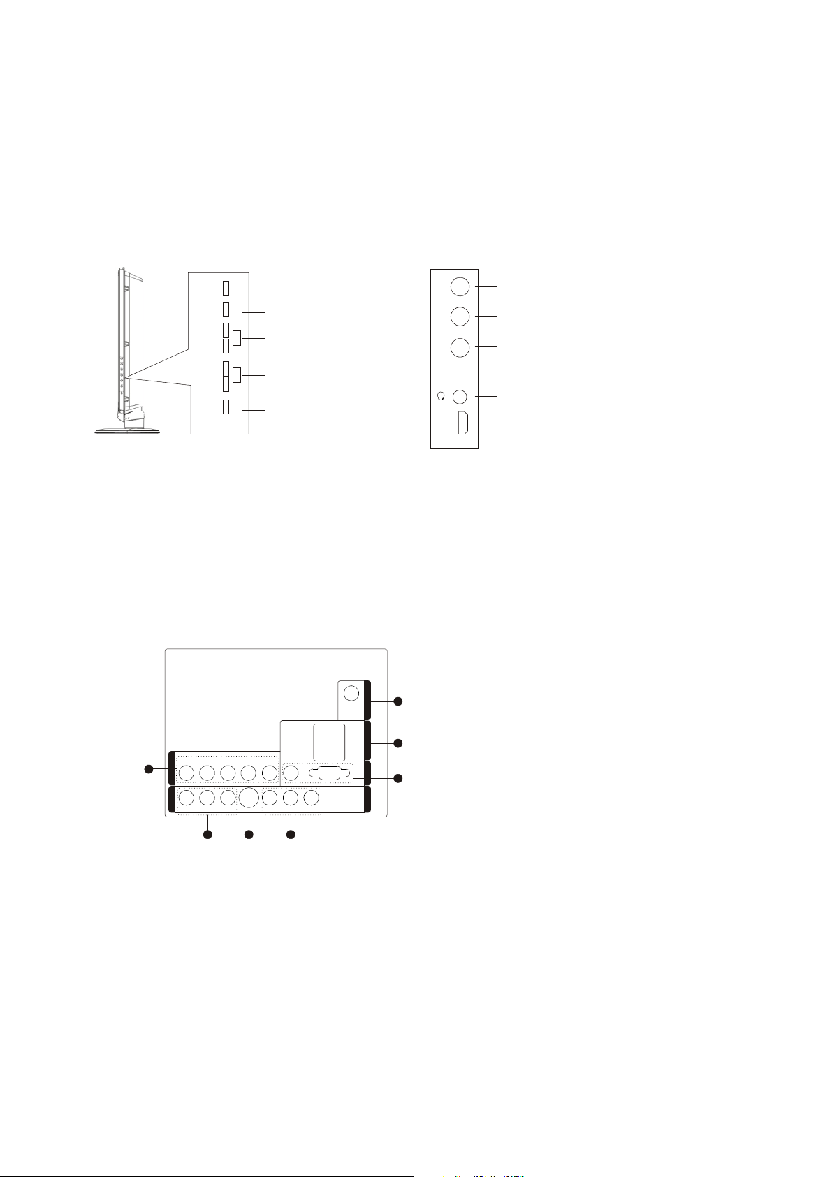
6. Operation Instructions
Basal information
6-1 Front panel controls
Side
TV/AV
MENU
VOL+
VOL-
CH+
CH-
POWER
1
2
3
4
5
1. TV/AV button
2. MENU button
3. VOL+/- : Volume decrease/increase,adjusting the menu
4. CH+/- : Channel number decrease/ increase
5. Power button
6-2 Rear panel controls
Side AV
L - AUDIO -RVIDEO 2HDMI 1
Right audio input
Left audio input
Video input
Earphone jack
HDMI input
5
6
7
AV OUT VGA IN HDMI2 IN ANT IN
Y Pb/Cb Pr/Cr L-AUDIO-R
1
CONMPENT IN
Av1 IN
VIDEO1 L-AUDIO-R S-VIDEO VIDEO L-AUDIO-R
2
Component Input
1.
VGA/DTV
AUDIO
3
4
VGA
Connect a component video/audiodevice to these jacks
Input
2.AV1
Connect audio/video out from an audio/video device to these jacks
S-Video Input
3.
Connect S-Video out from a S-Video device to these jacks
Video/Audio output terminal
4.
Connect ordinary video/audio or other appliance audio input terminals
Antenna Input
5.
Connect cable or antenna signals to the TV, either directly or through your cable box
6.
HDMI Input
Connnect a signal to HDMI
7.VGA Input
Connect the monitor output connector from a PC to the jack
19
Page 20
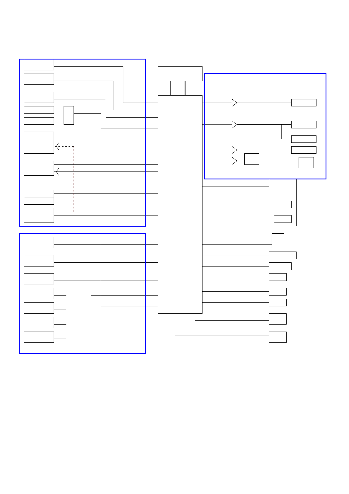
VIDEO INPUT&OUTPUT MODULE
HDMI1
HDMI2
AUDIO OUT MODULE
DDR SDRAM(128M,16BIT)
ADDR DATA
VGA
YPbPr1
DVB(option)
YPbPr2
SCART1/AV1
SCART2
SCART1OUT
SCART2OUT
AV2(CVBS)
S-VIDEO1(Y/C)
VGA AUDIO
HDTV1 AUDIO
SCART1/AV1 AUDIO
330
(option)
R/L
R/L
R/L
DVIRX0
DVIRX1
R1,G1,B1,Hs,Vs
R2,G2,B2
R0,G0,B0
CVBS2
CVBS3
Y0,C0
CVBSOUT
CVBS1
Y1,C1
CVBS0
SIF0
AUR/L0
AUR/L1
AUR/L2
MST6X89CL
AUOUTR/L3
AUOUTR/L2
AUOUTR/L0
AUOUTR/L1
DC 12V/5V
LVDS
CTRL
5VSTB/3.3V/1.8V/2.5V
SAR
IR/GPIO
UART/I2C
GAIN
GAIN
OP
OP
TFA9810T
24V
SCART1 OUT
SCART2 OUT
AV OUT(FOR CHINA)
HEADPHONE
SPEAKER
LCD PNL
INVERTER
PanelTV(RF)+9886
P0WER
KEYPAD BOARD
IR BOARD
DEBUG
SCART2/SUB AV AUDIO
AV2 AUDIO
R/L
R/L
4052
YPBPR2 AUDIO
DVB AUDIO
R/L
R/L
AUDIO IN MODULE
Power for ICs
AUR/L3
AUMONO
USB
CARD READER
EEPROMI2C
FLASHSPI
USB
CARD READER
21
Page 21
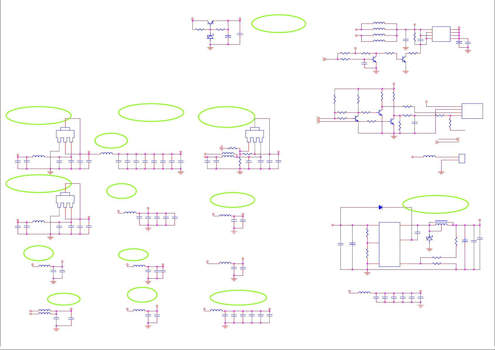
Vcc3.3for MST6X89CL
analog
U5
U5
AMS1117-3.3
AMS1117-3.3
5Vstb
C20
C20
0.1uF
0.1uF
C359
C359
10uF
10uF
L12 FBL12 FB
C21
C21
0.1uF
0.1uF
Vcc3.3for MST6X89CL
analog
U6
U6
AMS1117-3.3
AMS1117-3.3
+5V
C40
C40
0.1uF
0.1uF
+3.3AVDD
C384
C384
10uF
10uF
+3.3AVDD
for AVDD_SIF
+3.3AVDD
+3.3Vstb
L14 FBL14 FB
L19 FBL19 FB
L49 FBL49 FB
C33
C33
0.1uF
0.1uF
C372
C372
10uF
10uF
3.3V for
AVDDPLL2
ADJ
OUT
ADJ
OUT
1
ADJ
OUT
ADJ
OUT
1
AVDD_SIF
C49
C49
0.1uF
0.1uF
AVDD_MemPLL
C371
C371
10uF
10uF
Q41
Q41
3904
3904
23
R154
R154
NC/0
NC/0
1
R157
R157
220
220
D1349VD134
9V
WARNING !!!
PWM2 DUTY MUST BE 0x30(CANN'T >0x40,BK0_C7=0x30),
or will destroy Q44!!!!!!!!!!!!!!!
Vcc3.3for MST6X89CL
analog
4
C357
C357
10uF
10uF
C61
C61
0.1uF
0.1uF
Pin99, Pin165,
Pin183, Pin194,
Pin207, Pin221,
Pin235,
C67
C67
C69
0.1uF
0.1uF
C69
0.1uF
0.1uF
C66
C66
0.1uF
0.1uF
C65
C65
0.1uF
0.1uF
C68
C68
0.1uF
0.1uF
VDDP
C70
C70
0.1uF
0.1uF
IN
IN
3
2
C22
C22
C360
C360
0.1uF
0.1uF
10uF
10uF
+3.3Vstb
C361
C361
10uF
10uF
+3.3V for
VDDP
L17 FBL17 FB
2.5V for MST6X89CL
and DDRAM
60mA
5Vstb
+5V
C31
C31
0.1uF
0.1uF
L50 NCL50 NC
L13 FBL13 FB
C379
C379
10uF
10uF
CA14
CA14
100uF/16V
100uF/16V
AMS1117-2.5
AMS1117-2.5
R75 0R75 0
+9V+12V
+9V for 74HC4052 SWITCH AUDIO
C147
C147
0.1uF
0.1uF
4
ADJ
OUT
ADJ
OUT
IN
R730R73
0
1
C24
C24
0.1uF
0.1uF
IN
3
2
C374
C374
10uF
10uF
C25
C25
0.1uF
0.1uF
+2.5VM
C375
C375
10uF
10uF
U8
U8
R74 NCR74 NC
LCD Power
L5
L5
NC/600(4.5X3.2)
NC/600(4.5X3.2)
L2
+12V
+5V_Pnl
5Vstb
R10
R10
10K
R444
R444
10K
10K
R21 0R21 0
R17 NCR17 NC
10K
R5
4.7KR54.7K
1
ON_PANEL
ON_PANEL2
PWM0
ON_PBACK
PWM0
ON_PBACK2
L2
L6
L6
L27
L27
R15 10KR15 10K
1
C15
C15
0.1uF
0.1uF
R18NCR18
NC
R13
R13
4.7K
4.7K
Q5
NC(3904)Q5NC(3904)
2 3
R16 4.7KR16 4.7K
NC/600(4.5X3.2)
NC/600(4.5X3.2)
600(4.5X3.2)
600(4.5X3.2)
600(4.5X3.2)
600(4.5X3.2)
R6 4.7KR6 4.7K
Q2
3904Q23904
2 3
R91KR9
1K
1
2 3
Q3
3904Q33904
1
5Vstb
R12
R12
220
220
Q4
3904Q43904
2 3
VPANEL_IN
R2
100KR2100K
C1
0.1uFC10.1uF
R3 10KR3 10K
Q1
1
2 3
3904Q13904
SAMSUNG panel 0~3.3V R34=10K
LG/CMO/AU panel 0~5V,R34 NC
R11 0R11 0
R14 1KR14 1K
R34
R34
NC/10K
NC/10K
+5V
U2
IRF7314U2IRF7314
1
S1
2
G1
3
S2
C2
4
G2
0.1uFC20.1uF
+5V
BL-ON/OFF
BL-ADJ_IN
C14
C14
2.2uF
2.2uF
BL-ADJ_IN
L11 600(4.5X3.2)L11 600(4.5X3.2)
R19 0R19 0
BL-ADJ_OUT
BL-ADJ_IN
D1
D1
D2
D2
CA21
CA21
100uF/16V
100uF/16V
R72NCR72
NC
BL-ADJ_OUT
VCC-Panel
8
7
6
5
4
3
2
1
BL-ADJ_OUT 2
2
1
C6
2.2uFC62.2uF
CON2
CON2
5V
GND
BRI_ON/OFF
BRI_ADJ
CON4_2.0
CON4_2.0
CN6
CN6
CON4_2.5
CON4_2.5
USB Power
4
IN
IN
3
2
C385
C385
10uF
10uF
C34
C34
0.1uF
0.1uF
+3.3AVDD
C386
C386
10uF
10uF
Pin63
60mA
+3.3AVDD for
AVDDA
Pin14, Pin39, Pin58,Pin254
+3.3Vstb
L23 FBL23 FB
C362
C362
10uF
10uF
+3.3V for
VDD_MPLL
+3.3Vstb AVDD_MPLL
L24 FBL24 FB
AVDDA
C58
C58
0.1uF
0.1uF
C370
C370
10uF
10uF
10nF
10nF
262mA 600mA
2.5V for DDRAM
C23
C23
0.1uF
0.1uF
C60
C60
1 2
0.1uF
0.1uF
C62
C62
C287
C287
0.1uF
0.1uF
C289
C289
0.1uF
0.1uF
10mA
+2.5VM +2.5V_DMC
+2.5VM
L21 FBL21 FB
L25 FBL25 FB
C376
C376
10uF
10uF
+2.5V_DMQ
C377
C377
10uF
10uF
C50
C50
0.1uF
0.1uF
C63
C63
0.1uF
0.1uF
5Vstb
C17
C17
0.1uF
0.1uF
CA8
CA8
+
+
100uF/16V
100uF/16V
R23
R23
12K
12K
R25
R25
8.2K
8.2K
U9
MP2359U9MP2359
VCC5OUT
4
EN
2
GND
D6
1N4148D61N4148
BST
Vcc 1.26V for MST6X89CL
6
1
3
FB
C16
C16
10nF
10nF
R86 110_1%R86 110_1%
R28 2.7K_1%R28 2.7K_1%
4.7uHL74.7uH
D8
1N5822D81N5822
L7
3
CA9
CA9
+
+
220uF/16V
220uF/16V
VCC-1.26V
C381
C381
C32
C32
0.1uF
0.1uF
10uF
10uF
54
12
R24
R24
1.5K_1%
1.5K_1%
0.81*(1+Rup/Rdown)=1.26V---Rup=1.5K, Rdown=2.7K
C28
C28
0.1uF
0.1uF
C29
C29
0.1uF
0.1uF
VDDC
C30
C30
Pin99, Pin146, Pin182,
Pin195, Pin242
0.1uF
0.1uF
C47
C47
0.1uF
0.1uF
Pin136
4mA
+3.3AVDD for
AVDD_AU
+3.3AVDD
L22 FBL22 FB
AVDD_AU
C373
C373
10uF
10uF
C51
C51
0.1uF
0.1uF
Pin70
30mA
+2.5V for MST6X89CL
L16 FBL16 FBL18 NCL18 NC
C378
C378
10uF
10uF
C35
C35
0.1uF
0.1uF
C36
C36
0.1uF
0.1uF
C37
C37
0.1uF
0.1uF
C38
C38
0.1uF
0.1uF
VCC-1.26V
L8 FBL8 FB
+2.5MVDD+2.5VM
30mA
C39
C39
Pin108, Pin114,
0.1uF
0.1uF
Pin119, Pin135, P147
C380
C380
10uF
10uF
C26
C26
0.1uF
0.1uF
C27
C27
0.1uF
0.1uF
22
Page 22
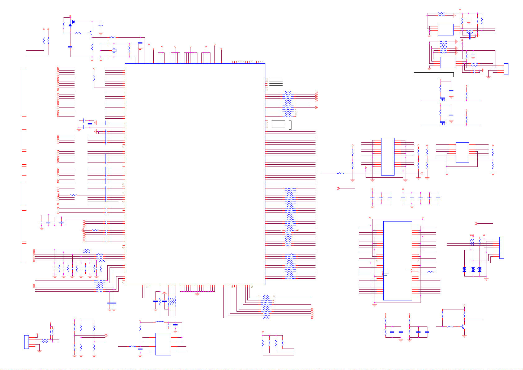
HDMI
INPUT
Y PB PR
INPUT
VGA
INPUT
Y,Pb,Pr
INPUT
VIDEO
INPUT
AUDIO
INPUT
AUDIO
OUTPUT
TXD0
RXD0
CON38
CON38
CON5_2.0
CON5_2.0
R234
R234
HDMI1_HPDCTRL
HDMI2_HPDCTRL
C436
C436
4.7uF
4.7uF
SC2-L
SC2-L
SC2-R
SC2-R
AMP-L
AMP-L
AMP-R
AMP-R
PH-L
PH-L
PH-R
PH-R
I2C_SDA
I2C_SCL
TXD0
RXD0
KEY0-in
KEY1-in
5Vstb
1
2
3
4
5
+3.3AVDDAVDDA
R235
R235
10K
10K
10K
10K
TX1CLKTX1CLK+
B1_TX0B1_TX0+
G1_TX1G1_TX1+
R1_TX2R1_TX2+
HDMI1_SDA
HDMI1_SCL
HDMI1_HPDCTRL
TX2CLKTX2CLK+
B2_TX0B2_TX0+
G2_TX1G2_TX1+
R2_TX2R2_TX2+
HDMI2_SDA
HDMI2_SCL
HDMI2_HPDCTRL
SCB+
SCG+
SC_SOG
SCR+
HS_RGB
VS_RGB
BIN+
SOG
GIN+
RIN+
PR+
SOY
Y+
PB+
SV1-Cin
SV1-Yin
AV3-Vin+
AV1-Vin+
TV1-Vin+
TV1-Vin-
CVBSOut
TV-SIFP
TV-SIFM
C435
C435
1uF
1uF
5Vstb
4.7K
4.7K
R367100 R367100
R368100 R368100
R384
R384
4.7K
4.7K
C213
C213
10uF
10uF
C188
C188
2.2nF
2.2nF
R394
R394
RXD0
TXD0
R26
R26
10K
10K
TX1CLKTX1CLK+
B1_TX0B1_TX0+
G1_TX1G1_TX1+
R1_TX2R1_TX2+
HDMI1_SDA
HDMI1_SCL
HDMI1_HPDCTRL
TX2CLK-
TX2CLK+
B2_TX0B2_TX0+
G2_TX1-
G2_TX1+
R2_TX2-
R2_TX2+
HDMI2_SDA
HDMI2_SCL
HDMI2_HPDCTRL
SCB+
SCG+
SC_SOG
SCR+
HS_RGB
VS_RGB
BIN+
SOG
GIN+
RIN+
PR+
SOY
Y+
PB+
SV1-Cin
SV1-Yin
AV3-Vin+
AV1-Vin+
R211 47R211 47
TV1-Vin+
TV1-Vin-
CVBSOut
C437
C437
0.1uF
0.1uF
C172
C172
R352
R352
2.2nF
2.2nF
22K
22K
VDDP
3
1
R170 1KR170 1K
C206
C206
10uF
10uF
PC-Lin
PC-Rin
HD1-Lin
HD1-Rin
AV1-Lin
AV1-Rin
MUX-Lin
MUX-Rin
TV1-L/Rin
C154
C154
R293
R293
10nF
10nF
22K
22K
+3.3Vstb
R460
R460
10K
10K
R423NCR423
NC
2
D54
D54
BAV99
BAV99
C812 0.1uFC812 0.1uF
C814
C814
R155 100R155 100
R156 100R156 100
C176
C176
R272
R272
10nF
10nF
22K
22K
R425NCR425
NC
R462
R462
10K
10K
Q14
Q14
1
3906
3906
SYS_RST
3 2
R172
R172
10K
10K
AVDDA
R454
R454
390_1%
390_1%
C813NCC813
NC
0.1uF
0.1uF
SCB+
SCG+
SC_SOG
SCR+
HS_RGB
VS_RGB
BIN+
SOG
GIN+
RIN+
PB+
SOY
Y+
PR+
SV1-Cin
SV1-Yin
AV3-Vin+
AV1-Vin+
AV2-VinTV1-Vin+
TV1-Vin-
CVBSOut2
CVBSOut
TV-SIFP
TV-SIFM
AUVREF
AUVRADP
AUVRADN
PC-Lin
PC-Rin
HD1-Lin
HD1-Rin
R663 0R663 0
AV1-Lin
AV1-Rin
MUX-Lin
MUX-Rin
TV1-L/Rin
R44 100R44 100
R42 100R42 100
R41 100R41 100
R40 100R40 100
R153
R153
C152
C152
C153
C153
R351
R351
22K
22K
10nF
10nF
10nF
10nF
22K
22K
RP27 RP100X4
RP27 RP100X4
8642
8642
R127 1KR127 1K
R128 1KR128 1K
R442
R442
10K
10K
PWM0
PWM1
PWM3
R469NCR469
NC
CA110
CA110
47uF/16V
47uF/16V
R27 1KR27 1K
C263
C263
27pF
27pF
C356
C356
27pF
27pF
TX1CLKTX1CLK+
B1_TX0B1_TX0+
G1_TX1G1_TX1+
R1_TX2R1_TX2+
HDMI1_HPDCTRL
HDMI1_SDA
HDMI1_SCL
TX2CLKTX2CLK+
HDMI2_HPDCTRL
HDMI2_SDA
HDMI2_SCL
C358 0.1uFC358 0.1uF
C815
C815
C816 0.1uFC816 0.1uF
C203 47nFC203 47nF
C202 47nFC202 47nF
C288 1nFC288 1nF
C201 47nFC201 47nF
C133 47nFC133 47nF
C136 1nFC136 1nF
C134 47nFC134 47nF
C135 47nFC135 47nF
C157 47nFC157 47nF
C159 1nFC159 1nF
C158 47nFC158 47nF
C156 47nFC156 47nF
C317 47nFC317 47nF
C316 47nFC316 47nF
C312 47nFC312 47nF
C311 47nFC311 47nF
C309 47nFC309 47nF
C308 47nFC308 47nF
C214 47nFC214 47nF
C440 0.1uFC440 0.1uF
C441 0.1uFC441 0.1uF
C332 2.2uFC332 2.2uF
C333 2.2uFC333 2.2uF
C334 2.2uFC334 2.2uF
C335 2.2uFC335 2.2uF
C434 0.1uFC434 0.1uF
C336 2.2uFC336 2.2uF
C337 2.2uFC337 2.2uF
C338 2.2uFC338 2.2uF
C339 2.2uFC339 2.2uF
C195 2.2uFC195 2.2uF
LINE_OUT_1L
LINE_OUT_1R
DAC_OUT_0R
DAC_OUT_1L
DAC_OUT_1R
R149
R149
22K
22K
7531
7531
SAR0
SAR1
PWM0
CL=20pf of XTAL
Y1
3
1 2
B2_TX0B2_TX0+
G2_TX1G2_TX1+
R2_TX2R2_TX2+
VCLAMP
REFP
REFM
0.1uF
0.1uF
VCOM3
VCOM2
BIN0P
GIN0P
SOGIN0
RIN0P
BIN1P
SOGIN1
GIN1P
RIN1P
BIN2P
SOGIN2
GIN2P
RIN2P
C1
Y1
CVBS3
CVBS2
VCOM1
CVBS0
VCOM0
SIF0P
SIFM
AUL0
AUR0
AUL1
AUR1
AUCOM
AUL2
AUR2
AUL3
AUR3
AUMONO
DAC_OUT_0L
C366100pF C366100pF
C367100pF C367100pF
12MHZY112MHZ
PWM1
252
253
255
256
177
178
179
180
171
172
173
174
9
RXACKN
10
RXACKP
12
RXA0N
13
RXA0P
15
RXA1N
16
RXA1P
18
RXA2N
19
RXA2P
20
HPLUGA
21
REXT
22
DDCDA_DA
23
DDCDA_CK
RXBCKN
RXBCKP
RXB0N
RXB0P
1
RXB1N
2
RXB1P
4
RXB2N
5
RXB2P
6
HPLUGB
7
DDCDB_DA
8
DDCDB_CK
26
VCLAMP
27
REFP
28
REFM
33
VCOM3
35
VCOM2
34
BIN0P
36
GIN0P
37
SOGIN0
38
RIN0P
41
HSYNC0
42
VSYNC0
24
HSYNC1
25
VSYNC1
29
BIN1P
30
SOGIN1
31
GIN1P
32
RIN1P
43
VSYNC2
44
BIN2P
45
SOGIN2
46
GIN2P
47
RIN2P
48
C1
49
Y1
50
C0
51
Y0
52
CVBS3
53
CVBS2
54
CVBS1
55
VCOM1
56
CVBS0
57
VCOM0
59
CVBSOUT1
60
CVBSOUT0
62
SIF0P
64
SIF1P
65
SIFM
69
AUVREF
68
AUVRADP
67
AUVRADN
71
AUL0
72
AUR0
73
AUL1
74
AUR1
75
AUCOM
76
AUL2
77
AUR2
78
AUL3
79
AUR3
80
AUMONO
81
AUOUTL3
82
AUOUTR3
83
AUOUTL2
84
AUOUTR2
85
AUOUTL1
86
AUOUTR1
87
AUOUTL0/Subwoofer
88
AUOUTR0
DDCR_DA
DDCR_CK
DDCA_DA
DDCA_CK
SAR0
SAR1
SAR2
SAR3
R52 33KR52 33K
U21
U21
A0
A1
A2
GND4SDA
24C04/24C128
24C04/24C128
0.1u/25V
0.1u/25V
1
Q201
Q201
32
BSS138LT1
BSS138LT1
1
Q202
Q202
32
BSS138LT1
BSS138LT1
RXO0RXO1RXO2RXOC-
RXO3RXO4-
C123
C123
0.1uF
0.1uF
R419
R419
4.7K
4.7K
R135 4.7KR135 4.7K
VCC
WP
SCL
C251
C251
0.1u/25V
0.1u/25V
LED-B
LED-R
VCC
WP
SCL
C252
C252
5Vstb
8
7
6
5
5Vstb
8
7
6
5
R258
R258
4.7K
4.7K
R266
R266
4.7K
4.7K
A0-1A0+
A1-3A1+
A2-5A2+
GND7GND
AC-9AC+
A3-11A3+
A4-13A4+
Select15Select
CON36
CON36
INPAQ_VPORT
INPAQ_VPORT
1
C306
C306
R475
R475
0.1uF
0.1uF
4.7K
4.7K
R308 100R308 100
R309 100R309 100
C239 47pFC239 47pF
C236 47pFC236 47pF
R484
R484
4.7K
4.7K
R358 100R358 100
R359 100R359 100
C240 47pFC240 47pF
C237 47pFC237 47pF
+3.3Vstb
3.3V_SCLSCL_EXT
+3.3Vstb
3.3V_SDA
CON9
CON9
2
4
6
8
10
12
14
16
IR-in
+3.3Vstb5Vstb
R429
R429
4.7K
4.7K
D132
D132
INPAQ_VPORT
INPAQ_VPORT
1 2
5Vstb
R413
R413
4.7K
4.7K
Q46
Q46
3904
3904
2 3
R471
R471
R470
R470
4.7K
4.7K
4.7K
4.7K
C313
C313
0.1uF
0.1uF
I2C_SCL
I2C_SDA
WP_KEY
RXO0+
RXO1+
RXO2+
RXOC+
RXO3+
RXO4+
5Vstb
R433
R433
R420
R420
8.2K
8.2K
8.2K
8.2K
IR-in
KEY1-in
KEY1-in
KEY0-in
D133
D133
D131
D131
1 2
1 2
INPAQ_VPORT
INPAQ_VPORT
LED-B
I2C_SDA
IR-in
WP_EEP
I2C_SCL
R495
R495
10K/NC
10K/NC
R496NCR496
NC
1
2
3
4
5
6
7
8
9
CON5_2.0
CON5_2.0
CON33
CON33
1
2
3
4
CON4-2.0
CON4-2.0
CN5
CN5
R102 NC/4.7KR102 NC/4.7K
R104 4.7KR104 4.7K
U43
U43
1
A0
2
A1
3
A2
GND4SDA
24C64
24C64
C150
C150
AVDD_AU
AVDD_SIF
248
70
AVDD_AU
HWRESET
PWM0/MCUCFG0
PWM1/MCUCFG1
PWM3/MCUCFG3
PWM2/MCUCFG2
175
176
192
191
PWM3
PWM0
PWM1
SPI_CZ
SPI_DO
WP_FLASH
AVDDA
14
39
58
254
63
AVDD_SIF
AVDD_DVI
AVDD_DVI
AVDD_ADC
AVDD_ADC
SCK
IRIN
167
182
SCK
C365100pF C365100pF
R453100 R453100
C387NC/10pF C387NC/10pF
IR-in
SPI_CK
L67 FBL67 FB
C352
C352
10uF
10uF
U42
U42
1
CE#
VDD
2
SO
HOLD#
3
WP#
SCK
VSS4SI
EN25F80-100/PMC25L080
EN25F80-100/PMC25L080
1nF
1nF
R4461MR446
1M
249
250
XIN
XOUT
+3.3Vstb
R464NCR464
NC
C364
C364
0.1uF
0.1uF
VDDC
101
149
165
185
193
240
VDDP
VDDP99VDDP
VDDC
VDDC
VDDC
VDDC
VDDC
MST6E89
MST6E89
GND
GND
GND
GND
SDI
SCZ
SDO
3
11
17
40
168
169
170
SDI
SDO
SCZ
RP19RP100X4
RP19RP100X4
8642
8642
7531
7531
SPI_DI
SPI_CZ
SPI_DO
C363
C363
0.1uF
0.1uF
8
7
SPI_CK
6
SPI_DI
5
VDDP
183
61
GND
AVDD_MemPLL
+2.5MVDD
AVDD_MPLL
96
136
251
AVDD_MEMPLL
GND
GND
257
AVDD_MPLL
GPIOB[6]
AD[0]
186
154
155
AD[1]
98
97
GPIOF[9]
AD[2]
156
157
GPIOF[8]
AD[3]
AD[4]
158
159
LVSYNC/GPIOE[0]
LVHSYNC/GPIOE[1]
AD[5]
AD[6]
AD[7]
WRZ
160
161
163
162
187
190
188
189
USB_DP
USB_DM
GPIOF[0]89GPIOF[1]90GPIOF[2]91GPIOF[3]92GPIOF[4]93GPIOF[5]94GPIOF[6]95GPIOF[7]
OTG_CID
OTG_VBUS
DI[13]
DI[12]
DI[11]
DI[10]
DI[9]
DI[8]
DI[7]
DI[6]
DI[5]
DI[4]
DI[3]
DI[2]
DI[1]
DI[0]
IVSYNC/TXD1
IHSYNC/RXD1
IDE
ICLK
LDE/GPIOE[2]
LCK/GPIOE[3]
LVB0M
LVB0P
LVB1M
LVB1P
LVB2M
LVB2P
LVBCKM
LVBCKP
LVB3M
LVB3P
LVB4M/NC
LVB4P/NC
LVA0M
LVA0P
LVA1M
LVA1P
LVA2M
LVA2P
LVACKM
LVACKP
LVA3M
LVA3P
LA4M/NC
LVA4P/NC
MDATA[0]
MDATA[1]
MDATA[2]
MDATA[3]
MDATA[4]
MDATA[5]
MDATA[6]
MDATA[7]
MDATA[8]
MDATA[9]
MDATA[10]
MDATA[11]
MDATA[12]
MDATA[13]
MDATA[14]
MDATA[15]
MCLK
MCLKZ
MCLKE
MVREF
UDQM
LDQM
DQS[0]
DQS[1]
RASZ
CASZ
WEZ
BARD[1]
BARD[0]
MADR[11]
MADR[10]
MADR[9]
MADR[8]
MADR[7]
MADR[6]
MADR[5]
MADR[4]
MADR[3]
MADR[2]
MADR[1]
MADR[0]
ALE
INT
RDZ
164
181
RP37 RP100X4
RP37 RP100X4
8642
8642
P42
P41
P40
P17
RP36 RP0X4
RP36 RP0X4
8642
8642
P16
P15
P14
P11
R457 100R457 100
P10
R451 100R451 100
P26
R136 100R136 100
5Vstb
R438
R438
4.7K
4.7K
AU2SD0
247
AU2SCK
246
AU2WS
245
AU2MCKO
244
243
242
GPOA7
239
GPOA6
238
GPIA5
237
GPOA4
236
GPOA3
234
GPOA2
233
GPOA1
232
GPOA0
231
IVSYNC
230
IHSYNC
229
GPOA25
228
GPIA24
227
LVSYNC
226
LHSYNC
225
LDE
224
LCK
223
220
219
218
217
216
215
214
213
212
211
210
209
206
205
204
203
202
201
200
199
198
197
196
195
123
122
121
120
118
117
116
115
112
111
110
109
107
106
104
103
130
129
128
MVREF
127
126
125
124
102
133
137
138
131
132
153
152
151
150
146
145
144
143
142
141
140
139
7531
7531
7531
7531
R435
R435
R432
R432
4.7K
4.7K
4.7K
4.7K
FOR I2S OUT
BK9_37[2]=0
RP23 100
RP23 100
RP22 100
RP22 100
RP38 100
RP38 100
RP28 RP100X4
RP28 RP100X4
RP29 RP100X4
RP29 RP100X4
RP30 RP100X4
RP30 RP100X4
RP31 RP100X4
RP31 RP100X4
RP32 RP33X4
RP32 RP33X4
R449 100R449 100
R450 100R450 100
R452 100R452 100
R483 100R483 100
R485 22R485 22
R486 22R486 22
R487 22R487 22
RP39 RP100X4
RP39 RP100X4
RP40 RP100X4
RP40 RP100X4
RP41 RP100X4
RP41 RP100X4
AU-SW1
AU-SW0
HP_DET
ON_PANEL
7531
8642
7531
8642
ON_PBACK
WP_KEY
WP_EEP
PW_CTL
7531
8642
7531
8642
7531
8642
7531
8642
TTL
Interface
7531
8642
7531
8642
7531
8642
7531
8642
7531
8642
7531
8642
7531
8642
7531
8642
7531
8642
7531
8642
7531
8642
7531
8642
7531
8642
7531
8642
7531
8642
7531
8642
Only 186 PIN can
used for ON USB.
R436
R436
SCL_RES
4.7K
4.7K
SDA_RES
SCL_EXT
SDA_EXT
RXO0RXO0+
RXO1RXO1+
RXO2RXO2+
RXOCRXOC+
RXO3RXO3+
RXO4RXO4+
RXE0RXE0+
RXE1RXE1+
RXE2RXE2+
RXECRXEC+
RXE3RXE3+
RXE4RXE4+
MDATA0
MDATA1
MDATA2
MDATA3
MDATA4
MDATA5
MDATA6
MDATA7
MDATA8
MDATA9
MDATA10
MDATA11
MDATA12
MDATA13
MDATA14
MDATA15
MCLK+
MCLKCKE
UDQM
LDQM
DQS0
DQS1
RASZ
CASZ
WEZ
BA1
BA0
AR11
AR10
AR9
AR8
AR7
AR6
AR5
AR4
AR3
AR2
AR1
AR0
LED-R
SCL_RES
SDA_RES
HDCEC
AMP-MUTE
SCL_EXT
SDA_EXT
ON_USB
AU-SW1
AU-SW0
HP_DET
ON_PANEL
ON_PBACK
PW_CTL
R141 NCR141 NC
BL-ADJ_IN
Only 181 PIN can used
for USB OTG_HOST_DET.
Only 159 Pin can used for
HDMI CEC funciton control.
HDCEC
AMP-MUTE
SCL_EXT
When use URAT1,AD2,AD3
SDA_EXT
Cann't be used again.
ON_USB
CON8
CON8
GND1GND
RXE0-
B0-3B0+
RXE1-
+5V_Pnl
R491
R491
10K/NC
10K/NC
3.3V_SDA
R492NCR492
VCC-Panel
NC
BL-ADJ_IN
MDATA15
MDATA14
MDATA13
MDATA12
MDATA11
MDATA10
MDATA9
MDATA8
DQS1
UDQM
WEZ
CASZ
RASZ
BA0
BA1 AR9
AR10
AR0
AR2 AR5
AR3
B1-5B1+
GND7GND
RXE2-
B2-9B2+
RXEC-
BC-11BC+
GND13GND
RXE3-
B3-15B3+
GND17GND
Select19Select
RXE4-
B4-21B4+
3Vsda233Vscl
GND25GND
VCC27VCC
VCC29VCC
adj in31adj out
CON36
CON36
+2.5V_DMC +2.5V_DMQ
C140
C140
C122
C122
C142
C142
0.1uF
0.1uF
0.1uF
0.1uF
0.1uF
0.1uF
+2.5V_DMC +2.5V_DMQ
U12
U12
1
MVDD
2
DQ0
3
VDDQ
4
DQ1
5
DQ2
6
VSSQ
7
DQ3
8
DQ4
9
VDDQ
10
DQ5
11
DQ6
12
VSSQ
13
DQ7
14
NC
15
VDDQ
16
LDQS
17
NC
18
MVDD
19
NC
20
LDM
21
WE
22
CAS
23
RAS
24
CS
25
NC
26
BA0
27
BA1
28
A10/AP
29
A0
30
A1
31
A2
32
A3
33
MVDD
HY5DU281622ET-4
HY5DU281622ET-4
+2.5V_DMQ +2.5MVDD
R209
R209
FSVREF
10K
10K
R243
R243
C121
C121
0.1uF
0.1uF
10K
10K
If 24C04,R214&R233 should be NC;
If 24C128, R158&R103 should be NC.
2
RXE0+
4
RXE1+
6
8
10
12
14
16
18
20
22
24
26
28
30
32
+3.3AVDD
RXE2+
RXEC+
RXE3+
RXE4+
3.3V_SCL
BL-ADJ_OUTBL-ADJ_IN
C141
C141
C138
C138
0.1uF
0.1uF
0.1uF
0.1uF
66
VSS
65
DQ15
64
VSSQ
63
DQ14
62
DQ13
61
VDDQ
60
DQ12
59
DQ11
58
VSSQ
57
DQ10
56
DQ9
55
VDDQ
54
DQ8
53
NC
52
VSSQ
51
UDQS
50
NC
49
VREF
48
VSS
47
UDM
46
CLK
45
CLK
44
CKE
43
NC
42
NC
41
A11
40
A9
39
A8
38
A7
37
A6
36
A5
35
A4
34
VSS
R655
R655
10K
10K
MVREF
R654
R654
C120
C120
1nF
1nF
10K
10K
108
114
119
135
194
VDDP
GND
66
147
207
221
235
VDDP
VDDP
VDDP
VDDM
VDDM
VDDM
VDDM
VDDM
U41
U41
GND
GND
GND
GND
GND
GND
GND
GND
GND
100
105
113
134
166
184
148
208
222
241
R158 4.7KR158 4.7K
R103 NC/4.7KR103 NC/4.7K
R473 4.7KR473 4.7K
R159 NC/4.7KR159 NC/4.7K
R214 NC/4.7KR214 NC/4.7K
R233 NC/4.7KR233 NC/4.7K
1
2
3
+3.3Vstb
R267
R267
100
100
+3.3Vstb
R268
R268
100
100
SDA_EXT
+5V_Pnl +3.3AVDD
R490
R490
R493
R493
10K/NC
10K/NC
10K/NC
10K/NC
R489NCR489
R494NCR494
NC
NC
BL-ADJ_OUT 1
C137
C137
C139
C139
0.1uF
0.1uF
0.1uF
0.1uF
MDATA0
MDATA1
MDATA2
MDATA3
MDATA4
MDATA5
MDATA6
MDATA7
DQS0
FSVREF
LDQM
MCLK-
R208
R208
MCLK+
150_1%
150_1%
CKE
AR11
AR8
AR7
AR6AR1
AR4
LED-R
C685
C685
C684
C684
1nF
1nF
0.1uF
0.1uF
23
Page 23
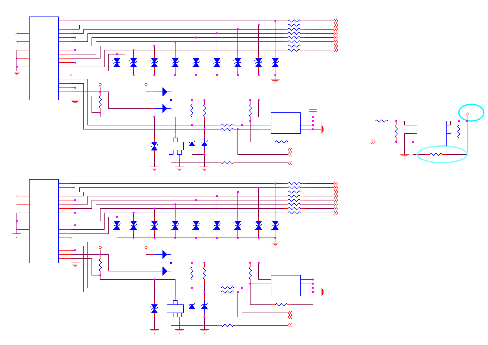
P1
P1
20
21
22
23
24
DATA2+
DATA2 SHIELD
DATA2-
DATA1+
GND1
DATA1 SHIELD
DAT1A-
GND2
DATA0+
DATA0 SHIELD
GND3
DATA0-
CLK+
GND4
CLK SHIELD
CLK-
GND5
CEC
NC
SCL
DDC/CEC GND
SDA
+5V POWER
HOT PLUG
HDMI_J
HDMI_J
1
2
3
4
5
6
7
8
9
10
11
12
13
14
15
16
17
18
19
CEC
HDMI1-RX2+
HDMI1-RX2HDMI1-RX1+
HDMI1-RX1HDMI1-RX0+
HDMI1-RX0HDMI1-RXC+
HDMI1-RXC-
INPAQ_VPORT
INPAQ_VPORT
HDMI1/5V
R781KR78
1K
HDMI1-HPD
HDMI1-DDC-SCL
HDMI1-DDC-SDA
D98
D98
1 2
INPAQ_EGA
INPAQ_EGA
D11
D11
1 2
INPAQ_EGA
INPAQ_EGA
+5V
1
2
INPAQ_VPORT
INPAQ_VPORT
1 2
1 2
D12
D12
D100
D100
D13
D13
1 2
INPAQ_EGA
INPAQ_EGA
D19
D19
3
BAT54C
BAT54C
Q8
Q8
C
C
23
23
SOT
SOT
B
B
132
1 2
INPAQ_EGA
INPAQ_EGA
R79
R79
10K
10K
D20
D20
5.6V
5.6V
E
E
1 2
3904
3904
D14
D14
INPAQ_EGA
INPAQ_EGA
R80
R80
10K
10K
D21
D21
5.6V
5.6V
1 2
D15
D15
1 2
R82 100R82 100
R83 100R83 100
1 2
INPAQ_EGA
INPAQ_EGA
1K1K
D16
D16
D17
D17
1 2
INPAQ_EGA
INPAQ_EGA
R81
R81
NC/4.7K
NC/4.7K
HDMI1_SCL
HDMI1_SDA
HDMI1_HPDCTRL
R310 10R310 10
R311 10R311 10
R312 10R312 10
R313 10R313 10
R314 10R314 10
R315 10R315 10
R696 10R696 10
R697 10R697 10
D18
D18
1 2
INPAQ_EGA
INPAQ_EGA
24C02=>EDID code must
be upto 256byte space,
for HDMI interface.
U14
U14
8
VCC
7
WP
6
SCL
5
R85 4.7KR85 4.7K
SDA
24C02
24C02
GND
R1_TX2+
R1_TX2G1_TX1+
G1_TX1B1_TX0+
B1_TX0TX1CLK+
TX1CLK-
C124
C124
1
NC
NC
NC
HDMI1_SCL 2
HDMI1_SDA 2
HDMI1_HPDCTRL 2
0.1uF
0.1uF
2
3
4
R1_TX2+ 2
R1_TX2- 2
G1_TX1+ 2
G1_TX1- 2
B1_TX0+ 2
B1_TX0- 2
TX1CLK+ 2
TX1CLK- 2
For CEC Leakage Protect
CEC
R664 0R664 0
HDCEC
HDCEC
U46 supplier must be 3.3V,When
power of,U46 supplier must be 0V
U46
R665
R665
NC/1K
NC/1K
U46
1
A
2
GND
3
B
R667 27KR667 27K
Must be 27K
V+
NC
SEL
6
5
4
R666
R666
10K
10K
FSA2156
FSA2156
+3.3AVDD
P7
P7
20
21
22
23
24
DATA2+
DATA2 SHIELD
DATA2-
DATA1+
GND1
DATA1 SHIELD
DAT1A-
GND2
DATA0+
DATA0 SHIELD
GND3
DATA0-
CLK+
GND4
CLK SHIELD
CLK-
GND5
CEC
NC
SCL
DDC/CEC GND
SDA
+5V POWER
HOT PLUG
HDMI_J
HDMI_J
1
2
3
4
5
6
7
8
9
10
11
12
13
14
15
16
17
18
19
CEC
HDMI2-RX2+
HDMI2-RX2HDMI2-RX1+
HDMI2-RX1HDMI2-RX0+
HDMI2-RX0HDMI2-RXC+
HDMI2-RXC-
INPAQ_VPORT
INPAQ_VPORT
HDMI2/5V
R1631KR163
1K
HDMI2-HPD
HDMI2-DDC-SCL
HDMI2-DDC-SDA
D102
D102
1 2
INPAQ_EGA
INPAQ_EGA
D38
D38
1 2
INPAQ_EGA
INPAQ_EGA
+5V
1
2
INPAQ_VPORT
INPAQ_VPORT
1 2
1 2
D37
D37
D103
D103
D22
D22
1 2
INPAQ_EGA
INPAQ_EGA
D34
D34
3
BAT54C
BAT54C
Q13
Q13
C
C
23
23
SOT
SOT
B
B
132
1 2
INPAQ_EGA
INPAQ_EGA
R93
R93
10K
10K
D36
D36
5.6V
5.6V
E
E
1 2
3904
3904
D24
D24
INPAQ_EGA
INPAQ_EGA
R138
R138
10K
10K
D35
D35
5.6V
5.6V
1 2
D25
D25
1 2
R94 100R94 100
R161 100R161 100
R137 1KR137 1K
1 2
INPAQ_EGA
INPAQ_EGA
D26
D26
D32
D32
1 2
INPAQ_EGA
INPAQ_EGA
R152
R152
NC/4.7K
NC/4.7K
HDMI2_SCL
HDMI2_SDA
HDMI2_HPDCTRL
R354 10R354 10
R350 10R350 10
R340 10R340 10
R356 10R356 10
R383 10R383 10
R385 10R385 10
R353 10R353 10
R355 10R355 10
D33
D33
1 2
INPAQ_EGA
INPAQ_EGA
24C02=>EDID code must
be upto 256byte space,
for HDMI interface.
U20
U20
8
VCC
7
WP
6
SCL
5
R160 4.7KR160 4.7K
SDA
24C02
24C02
GND
R2_TX2+
R2_TX2G2_TX1+
G2_TX1B2_TX0+
B2_TX0TX2CLK+
TX2CLK-
C132
C132
1
NC
NC
NC
HDMI2_SCL 2
HDMI2_SDA 2
HDMI2_HPDCTRL 2
0.1uF
0.1uF
2
3
4
R2_TX2+ 2
R2_TX2- 2
G2_TX1+ 2
G2_TX1- 2
B2_TX0+ 2
B2_TX0- 2
TX2CLK+ 2
TX2CLK- 2
24
Page 24
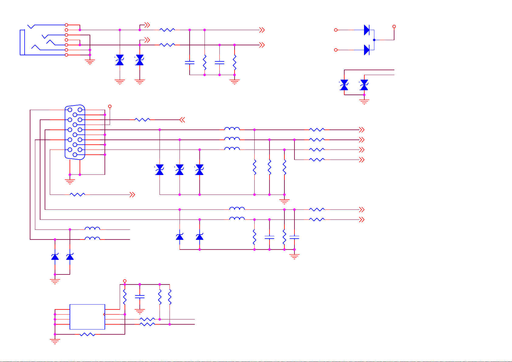
P2
P2
PHONEJACK
PHONEJACK
4
2
1
3
5
6
7
P3
15
14
13
12
11
16
17
VGAP3VGA
R111 NCR111 NC
5
10
4
9
3
8
2
7
1
6
PC-L
PC-R
INPAQ_VPORT
INPAQ_VPORT
VGA/5V
1 2
VGA-G+
VGA-R+
TXD0
D86
D86
PC-L
R3961KR396
PC-R
D87
D87
R3971KR397
1 2
INPAQ_VPORT
INPAQ_VPORT
R113 NCR113 NC
INPAQ_VPORT
INPAQ_VPORT
TXD0
1K
1K
RXD0
D95
D95
1 2
1 2
INPAQ_VPORT
INPAQ_VPORT
R294
R294
C260
C260
22K
22K
560pF
560pF
RXD0
D96
D96
INPAQ_VPORT
INPAQ_VPORT
D97
D97
1 2
C259
C259
R295
R295
560pF
560pF
22K
22K
L38 0L38 0
L39 0L39 0
L40 0L40 0
PC-Lin
PC-Rin
R9975R99
75
PC-Lin 2
PC-Rin 2
R10075R100
75
R10175R101
75
VGA/5V
+5V
INPAQ_VPORT
INPAQ_VPORT
R9547R95
R9647R96
R9747R97
R98 470R98 470
47
47
47
1 2
BIN+VGA-B+
GIN+
RIN+
SOG
D23
D23
1
2
BAT54C
BAT54C
D99
D99
VGA-DDC-5V
3
TXD0
RXD0
D101
D101
INPAQ_VPORT
INPAQ_VPORT
1 2
BIN+ 2
GIN+ 2
RIN+ 2
SOG 2
D29
D29
5.6V
5.6V
1 2
1
2
3
L43 FBL43 FB
L44 FBL44 FB
D31
D31
5.6V
5.6V
1 2
U16
U16
NC
NC
NC
GND4SDA
R116 4.7KR116 4.7K
VCC
VCLK
SCL
VGA-HS
VGA-VS
VGA-SDA
VGA-SCL
VGA-DDC-5V
8
7
6
5
24C02
24C02
R112NCR112
C145
C145
0.1uF
0.1uF
NC
R114 100R114 100
R115 100R115 100
R109
R109
4.7K
4.7K
R110
R110
4.7K
4.7K
VGA-SCL
VGA-SDA
D27
D27
5.6V
5.6V
1 2
D28
D28
5.6V
5.6V
1 2
L41 FBL41 FB
L42 FBL42 FB
25
R107
R107
2.2K
2.2K
C143NCC143
NC
R108
R108
2.2K
2.2K
C144NCC144
NC
R105 100R105 100
R106 100R106 100
HS_RGB
VS_RGB
HS_RGB 2
VS_RGB 2
Page 25
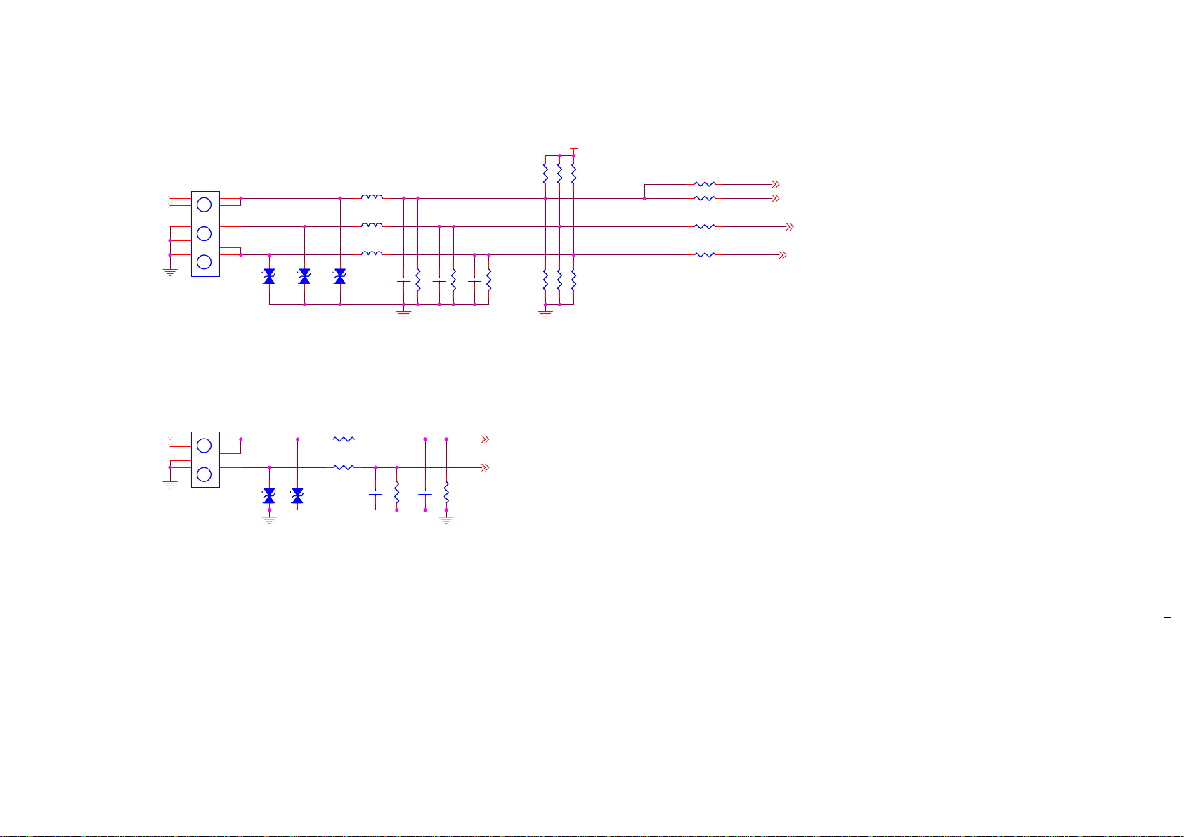
10
P4
P4
9
1
4
6
P5
P5
7
6
1
3
YPBPR
YPBPR
889
Y
Y
7
10
1
5
Pb
Pb
4
2
3
6
Pr
Pr
YPBPR_L/R
YPBPR_L/R
4
7
L
L
6
5
1
3
2
R
R
INPAQ_VPORT
INPAQ_VPORT
YPBPR1 Input
HD1_Y
7
HD1_Pb
5
2
HD1_Pr
3
4
5
2
D89
D89
1 2
INPAQ_VPORT
INPAQ_VPORT
HD1-L
D105
D105
1 2
INPAQ_VPORT
INPAQ_VPORT
D90
D90
1 2
INPAQ_VPORT
INPAQ_VPORT
R371 1KR371 1K
R372 1KR372 1K
D104
D104
INPAQ_VPORT
INPAQ_VPORT
1 2
L46 0L46 0
L47 0L47 0
L48 0L48 0
D91
D91
1 2
C200
C200
560pF
560pF
R215
R215
22K
22K
+5V
R119
R119
NC/10K
R118
R118
NC/10K
NC/10K
R133
R133
NC/10K
NC/10K
NC/10K
HD1_YIN
HD1_PBIN
HD1_PRIN
R134
R134
NC/10K
NC/10K
R125 47R125 47
R126 470R126 470
R124 47R124 47
R123 47R123 47
Y+
SOY
PR+
PB+
Y+ 2
SOY 2
PB+ 2
PR+ 2
R117
R117
NC/10K
NC/10K
R13075 R13075
C164NC C164NC
R212
R212
22K
22K
HD1-Lin
HD1-RinHD1-R
R13175 R13175
HD1-Lin 2
HD1-Rin 2
R132
R132
NC/10K
NC/10K
R12975 R12975
C163NC C163NC
C162NC C162NC
C198
C198
560pF
560pF
26
Page 26
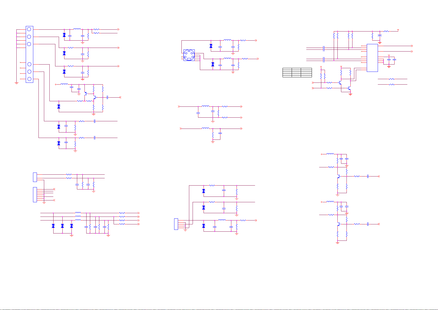
AV1 Input/output
P15
P15
13
14
15
16
AV1-V AV1-Vin+
7
AV in
AV in
1
7
2
AV1-L
8
L
L
3
8
4
AV1-R
9
R
R
5
9
6
13
10
AV out
AV out
10
14
11
L
L
11
15
12
R
R
12
16
AV6
AV6
USB YPBPR2 Input
CON24
CON24
2
HD2-L HD2-Lin
3
1
NC/CON3_2.0
NC/CON3_2.0
CON23
CON23
ON_USB
7
HD2_PBIN
6
HD2_YIN
5
4
HD2_PRIN
3
2
1
NC/CON7_2.0
NC/CON7_2.0
HD2_PRIN
HD2_YIN
HD2_PBIN
+5V
Scart2_Vout
INPAQ_VPORT
INPAQ_VPORT
Scart2_Lout
INPAQ_VPORT
INPAQ_VPORT
Scart2_Rout
INPAQ_VPORT
INPAQ_VPORT
IR-in
D122
D122
1 2
INPAQ_VPORT
INPAQ_VPORT
1 2
INPAQ_VPORT
INPAQ_VPORT
INPAQ_VPORT
INPAQ_VPORT
1 2
INPAQ_VPORT
INPAQ_VPORT
L68 FBL68 FB
D119
D119
1 2
D120
D120
1 2
D121
D121
1 2
R401 10KR401 10K
R386 10KR386 10K
ON_USB 2
IR-in 2
D123
D123
1 2
INPAQ_VPORT
INPAQ_VPORT
D116
D116
C180
C180
NC/330pF
NC/330pF
R374 1KR374 1K
D117
D117
1 2
R373 1KR373 1K
D118
D118
C519
C519
1nF
1nF
C520
C520
1nF
1nF
1 2
INPAQ_VPORT
INPAQ_VPORT
L580L58
0
C353
C353
C192
C192
10uF
10uF
0.1uF
0.1uF
R19968R199
R407 100R407 100
R204
R204
10K
10K
R408 100R408 100
R205
R205
10K
10K
C293
C293
560pF
560pF
L73 0L73 0
L74 0L74 0
L75 0L75 0
D124
D124
C181
C181
NC/330pF
NC/330pF
C184
C184
560pF
560pF
C187
C187
560pF
560pF
68
R304
R304
12K
12K
NC/330pF
NC/330pF
Q17
Q17
3906
3906
3 2
R198
R198
C827
C827
R166 47R166 47
R16875R168
R339NCR339
75
R174
R174
22K
22K
R188
R188
22K
22K
R194
R194
470
470
1
Q18
Q18
3904
3904
2 3
390
390
R202
R202
100
100
C216 2.2uFC216 2.2uF
Location
Near RCA.
C218 2.2uFC218 2.2uF
HD2-RinHD2-R
R303
R303
C294
C294
12K
12K
560pF
560pF
C204
C204
R21975R219
NC/330pF
NC/330pF
75
Note:when SCR+,SCG+,SCB+ as scart RGB
input,R339(net SC_SOG,from AV input)must
be 470ohm,R305must be NC,else SCR+
SCB+ as HDTV input, R305(net SC_SOG,from
HDTV input)must be 470ohm,R339 must be NC.
AV1-Vin+ 2
SC_SOG
NC
AV1-Lin
AV1-Lin 2
AV1-Rin
AV1-Rin 2
Note: The IC's
CVBSOUT level is
0.5Vp-p when input
signal is 1Vp-p, so
it must multiply
R196
R196
signal by four (GAIN
X 4) for 2Vp-p output
15K
15K
CVBSOut
C307 10uFC307 10uF
1
R22075R220
75
R201
R201
C205
C205
NC/330pF
NC/330pF
4.7K
4.7K
CVBSOut 2
Scart2_L
Scart2_R
SCR+
R216 47R216 47
R217 47R217 47
R218 47R218 47
R22175R221
R305 470R305 470
Note:when SCR+
input,R339(net SC_SOG,from AV input)must
75
be 470ohm,R305must be NC,else SCR+
SCB+ as HDTV input, R305(net SC_SOG,from
HDTV input)must be 470ohm,R339 must be NC.
SCR+ 2
SCG+
SCG+ 2
SCB+
SC_SOG
SC_SOG 2
,
SCG+,SCB+ as scart RGB
,
SCG+
,
TV1-V7
,
SCG+
S-Video1 Input
SV1-C SV1-Cin
D109
D109
P12 DIN4_V
P12 DIN4_V
LC
LC
7
8
TV1-V TV1-Vin+
TV1-L/R
TV1-L/R7
32
1
4
5
6
0
C190
C190
NC/330pF
NC/330pF
INPAQ_VPORT
INPAQ_VPORT
INPAQ_VPORT
INPAQ_VPORT
L640L64
NC/330pF
NC/330pF
L66
L66
10K
10K
1 2
D110
D110
1 2
C191
C191
R200
R200
12K
12K
AV2
R370 1KR370 1K
D112
D112
1 2
INPAQ_VPORT
INPAQ_VPORT
R369 1KR369 1K
D111
D111
1 2
INPAQ_VPORT
CON16
CON16
CON5_2.0
CON5_2.0
5
4
3
2
1
,
INPAQ_VPORT
AV3-V
INPAQ_VPORT
INPAQ_VPORT
L61 0L61 0
D113
D113
C185
C185
NC/330pF
NC/330pF
1 2
0
C207
C207
NC/330pF
NC/330pF
0
C215
C215
NC/330pF
NC/330pF
R192 47R192 47
R19375R193
75
R195 47R195 47
C256
C256
560pF
560pF
C193
C193
560pF
560pF
C189
C189
560pF
560pF
CA15
CA15
+9V
C320
C320
0.1uF
0.1uF
R191 NCR191 NC
R224 NCR224 NC
+9V
MUX-Lin
MUX-Lin 2
MUX-Rin
MUX-Rin 2
C323
C323
10uF
10uF
MUX-Lin
MUX-Rin
1
5
2
4
9
U28
U28
X0
X1
X2
X3
Y0
Y1
Y2
Y3
A
B
74HC4052
74HC4052
R177
R177
10K
10K
VCC
GND
SC2-L
SC2-R
VEE
X
Y
INH
R190 10KR190 10K
100uF/16V
100uF/16V
13
3
16
8
6
7
AV3-Lin
AV3-Rin
SC2-L 2
SC2-R 2
47K
L760L76
R222 47R222 47
R22575R225
C826
C826
NC/330pF
NC/330pF
75
L780L78
R228 47R228 47
R23075R230
C217
C217
NC/330pF
NC/330pF
75
TV1-Vin-
TV1-L/Rin
R197
R197
22K
22K
R189
R189
22K
22K
R186 47R186 47
C186
C186
R18775R187
75
NC/330pF
NC/330pF
TV1-Vin+ 2
TV1-Vin- 2
TV1-L/Rin 2
SV1-YinSV1-Y
AV3-RinAV3-R
AV3-LinAV3-L
AV3-Vin+
SV1-Cin 2
SV1-Yin 2
AV3-Vin+ 2SCB+ 2
AU-SW1 AU-SW0 Output
0
0 X3,Y3
01
1
11
X2,Y2
0
X1,Y1
X0,Y0
AU-SW02
AU-SW12
HD2-Lin
AV3-Lin
HD2-Rin
AV3-Rin
C325 2.2uFC325 2.2uF
C326 2.2uFC326 2.2uF
C329 2.2uFC329 2.2uF
C330 2.2uFC330 2.2uF
AU-SW0
AU-SW1
+9V
+9V
+5V
Scart2_L
Scart2_R
R242
R242
10K
10K
R176 47KR176 47K
R244
R244
10K
10K
R179 10KR179 10K
R183 10KR183 10K
L65 FBL65 FB
R681 47R681 47
L63 FBL63 FB
R687 47R687 47
47K
R223
R223
1
R173 47KR173 47K
R180 47KR180 47K
12
14
15
11
+9V
R680
R680
4.7k
4.7k
Q45
Q45
3904
3904
2 3
R68447R684
47
R686
R686
4.7k
4.7k
Q38
Q38
3904
3904
2 3
R69047R690
47
SW0
10
SW1
R206
R206
R182
R182
10K
10K
10K
10K
Q20
Q20
3904
3904
2 3
Q35
Q35
1
3904
3904
2 3
C819
C819
C351
C351
0.1uF
0.1uF
10uF
10uF
R682
R682
C348 2.2uFC348 2.2uF
R683 15kR683 15k
47k
47k
1
R685
R685
8.2k
8.2k
C820
C820
C350
C350
0.1uF
0.1uF
10uF
10uF
R688
R688
C349 2.2uFC349 2.2uF
R689 15kR689 15k
47k
47k
1
R691
R691
8.2k
8.2k
27
Page 27
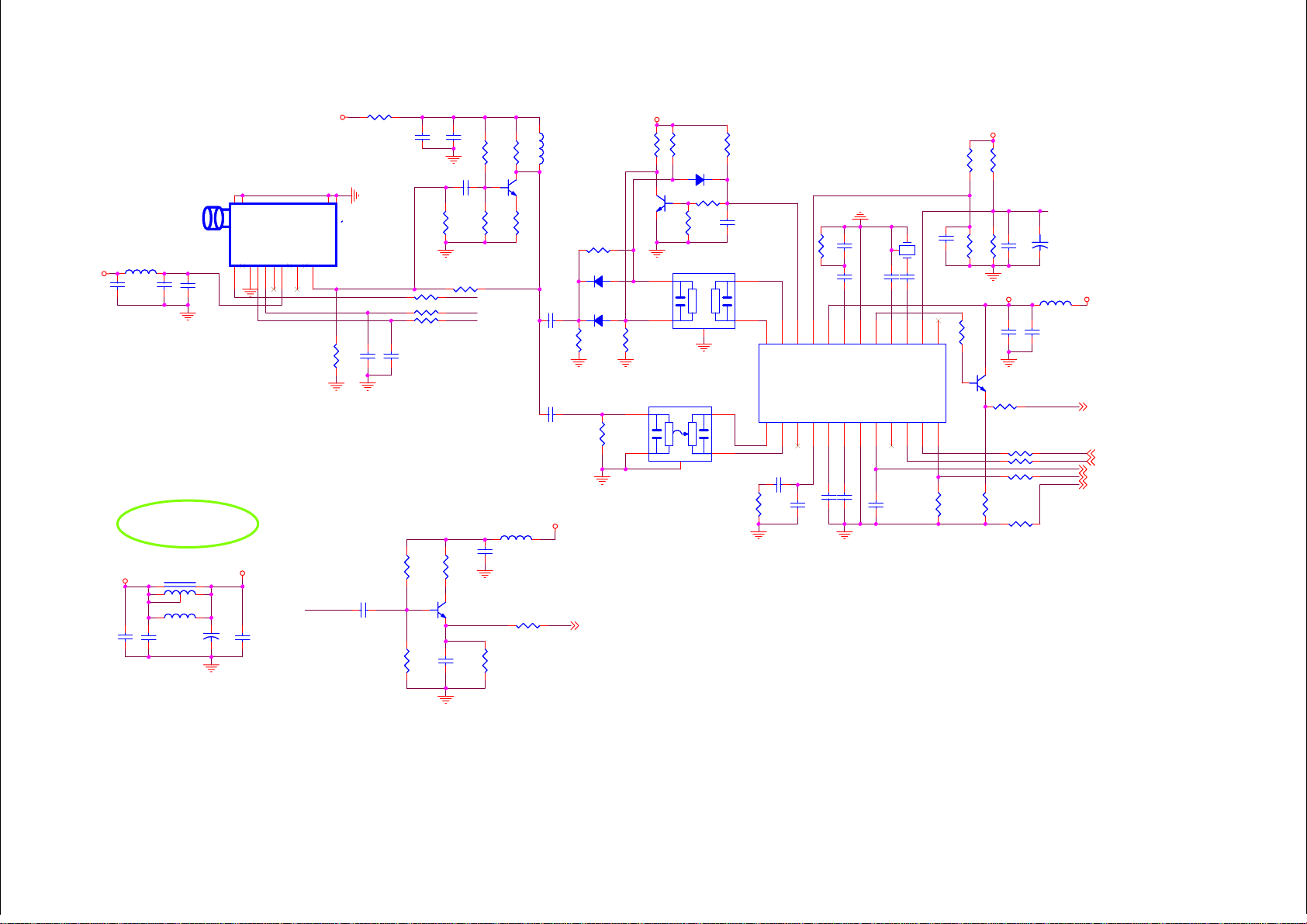
5V-IF
L81 FBL81 FB
C299
C300
C300
10uF
10uF
C299
10uF
10uF
AGND
C226
C226
0.1uF
0.1uF
5V and 12V for Tuner
C248
C248
0.1uF
0.1uF
L9
100uHL9100uH
3
L100NCL100
NC
100uF/16V
100uF/16V
54
12
+5V
C304
C304
10uF
10uF
15
GND114GND4
AGC1NC12AS3SCL4SDA55VA65VB7NC3833V9NC410IFout
5V-IF
C482
C482
C249
C249
0.1uF
0.1uF
U22
U22
TUNER_IF
TUNER_IF
11
SIFPOUT
+12V
13
R241NCR241
NC
R277 100R277 100
AGND
GND312GND2
IF_TV
C230
C230
22pF
22pF
AGND
C257 10nFC257 10nF
R251 100R251 100
R3801KR380
1K
R3811KR381
1K
C149
C149
10uF
10uF
R34775R347
75
R279 NC/0R279 NC/0
R250 0R250 0
R252 100R252 100
C233
C233
22pF
22pF
R69810R698
10
1
C247
C247
AGND
IF-AGC
SDA_EXT
SCL_EXT
32
22pF
22pF
C148
C148
10nF
10nF
10nF
10nF
Q40
Q40
3904
3904
1.2K
1.2K
R379
R379
820
820
C146
C146
R269
R269
AGND
R342
R342
4.7K
4.7K
1
R34556R345
C261
C261
0.1uF
0.1uF
R246
R246
56(220)
56(220)
3
Q28
Q28
2SC2216
2SC2216
2
56
L87
L87
10uH
10uH
R699 0R699 0
U23 PIN2 connected to PIN1 B/G,DK,I,L
U23 PIN2 connected to GND L'
L26
L26
0.82uH
0.82uH
R387 0R387 0
D79
D79
C229
C229
D65 BA277D65 BA277
R255
R255
10nF
10nF
4.7K
4.7K
AGND
C235
C235
10nF
10nF
AGND
5V-IF
TV-SIFP
0/BA277
0/BA277
AGND
R256NCR256
NC
5V-IF
R236
R236
4.7K
4.7K
Q22
Q22
3904
3904
2 3
AGND
1
2
R273NCR273
NC
IN
1
2
ING4OUT1
R237
R237
4.7K
4.7K
D88 NC/BA277D88 NC/BA277
R382 10KR382 10K
1
R245NCR245
NC
U23
U23
IN
OUT2
SAW
SAW
ING4OUT1
GND
3
K9453D
K9453D
AGND
U25
U25
K3953D
K3953D
OUT2
SAW
SAW
GND
3
R238
R238
4.7K
4.7K
C221
C221
10nF
10nF
5
24
5
VIF11VIF2
C241
C241
R262
R262
10nF
10nF
5.6K
5.6K
AGND AGND
C222
C222
R247
R247
1.5nF
1.5nF
330
330
21
22
AFC
SIF123SIF2
OUT2
OUT1
FMPLL
2
3
4
C243
C243
390pF
390pF
I2C ADDRESS(R263 NC):
READ is 0X87
WRITE is 0X86
20
VPP
DEEM
5
C245
C245
10nF
10nF
AGND
19
VPLL
AFD
6
C246
C246
470nF
470nF
C227
C227
C225
C225
470nF
470nF
220nF
220nF
17
18
AGND
DGND7TOP
C244
C244
1nF
1nF
Y2
4MHzY24MHz
3
16
CVBS
NC(5)/VAGC(6)
AUD_OUT8SDA
9
1 2
C228
C228
22pF
22pF
15
10
R239
R239
22K
22K
C223
C223
0.1uF
0.1uF
R248
R248
22K
22K
TV
R253
R253
14
13
100
100
NC
REF
TAGC
1
U24
U24
TDA9885&6
TDA9885&6
SCL
SIOMAD
11
12
SIFPOUT
R263
R263
NC(2K)
NC(2K)
R249
R249
100K
100K
AGND
5V-IF
32
R264
R264
Q23
Q23
3904
3904
220
220
R240
R240
22K
22K
IF-AGC
C224
C224
0.1uF
0.1uF
5V-OUT
C231
C231
0.1uF
0.1uF
AGND
R25775R257
75
R259 100R259 100
R260 100R260 100
R261 NCR261 NC
R265 0R265 0
CA71
CA71
+
+
47uF/16V
47uF/16V
L82FBL82
FB
C303
C303
10uF
10uF
TV1-V
TV1-L/R
TV-SIFP
TV-SIFM
SCL_EXT
SDA_EXT
5V-IF
TV1-V 6
SCL_EXT 2
SDA_EXT 2
TV1-L/R 6
TV-SIFP 2
TV-SIFM 2
AGND
28
Page 28
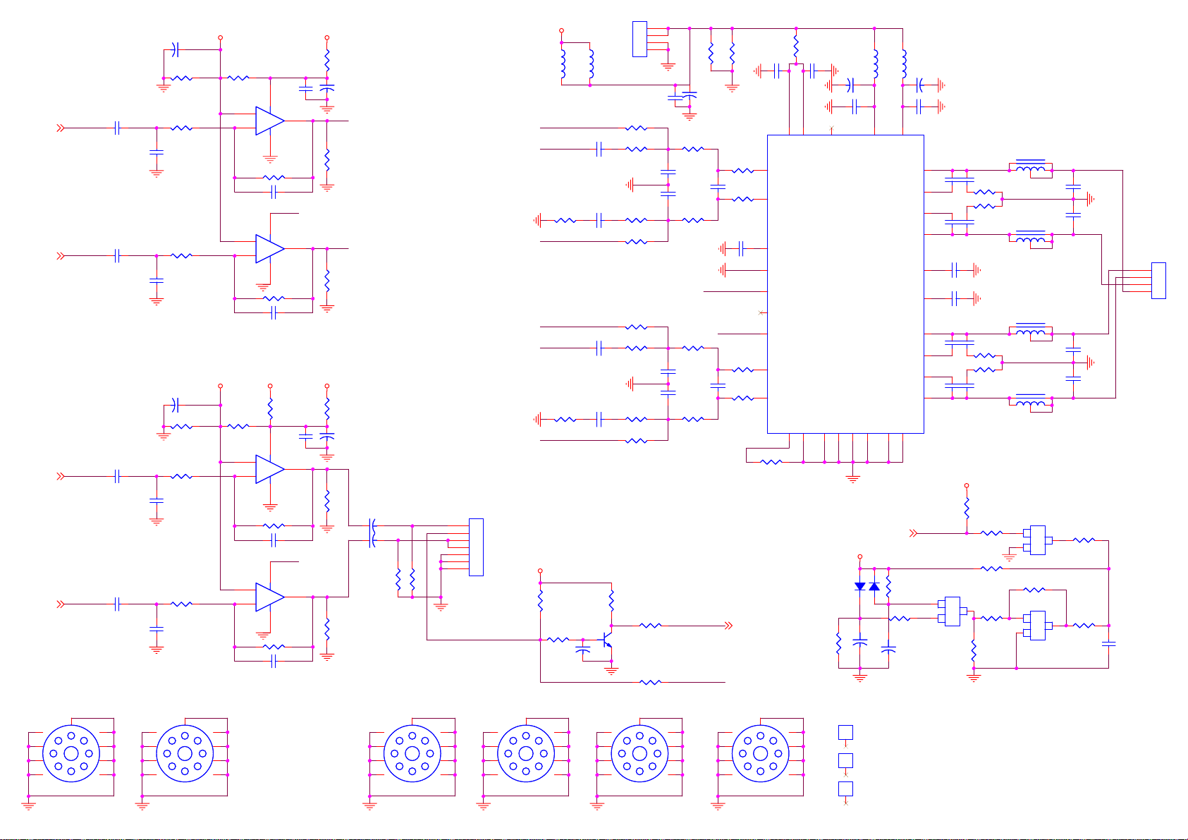
CON39
+12V6VBuf1
R437
0.1uF
0.1uF
1
TL062
TL062
U45B
U45B
7
TL062
TL062
OP_VCC2
0.1uF
0.1uF
1
7
C341
C341
C199
C199
R437
100
100
CA17
CA17
100uF/16V
100uF/16V
AMP-Lin
R402
R402
47K
47K
AMP-Rin
R403
R403
47K
47K
R430NCR430
NC
CA19
CA19
100uF/16V
100uF/16V
R404
R404
47K
47K
CA93 100uF/16VCA93 100uF/16V
R405
R405
47K
47K
For 26dB change R5, R14, R17 and
R26 from 100k into 200k.
* = R35 and R36 need to have the
same value as the output
impedance of the signal source.
P8
P8
3
5
2
4
1
6
7
CON5_2.0
CON5_2.0
R3011KR301
1K
PH-Lout
PH-Rout
R3021KR302
1K
CA16
CA16
100uF/16V
100uF/16V
R414
R414
AMP-L
AMP-R
PH-L
PH-R
C340 2.2uFC340 2.2uF
C343 2.2uFC343 2.2uF
C273 2.2uFC273 2.2uF
C272 2.2uFC272 2.2uF
AMP-L2
AMP-R2
PH-L2
PH-R2
R439 10KR439 10K
C342
C342
1nF
1nF
R441 10KR441 10K
C179
C179
1nF
1nF
CA18 100uF/16VCA18 100uF/16V
R410 33KR410 33K
R424 10KR424 10K
C194
C194
1nF
1nF
R422 10KR422 10K
C173
C173
1nF
1nF
33K
33K
R415 33KR415 33K
R411 33KR411 33K
OP_VCC1
U45A
U45A
84
3
+
+
2
-
-
R455 68KR455 68K
C479 100pFC479 100pF
OP_VCC1
84
5
+
+
6
-
-
R459 68KR459 68K
C478 100pFC478 100pF
+5V6VBuf2 +12V
R4270R427
0
U38A
U38A
84
3
+
+
2
-
-
PT2308
PT2308
R421 33KR421 33K
C464 100pFC464 100pF
OP_VCC2
U38B
U38B
84
5
+
+
6
-
-
PT2308
PT2308
R426 33KR426 33K
C473 100pFC473 100pF
+12V
L10
L10
OUT1-
AMP-Rin
R54 0R54 0
OUT1+
OUT2-
AMP-Lin
R65 0R65 0
OUT2+
+5V
R412
R412
10K
10K
R328 4.7KR328 4.7K
CA20
CA20
100uF/16V
100uF/16V
L31
L31
600(4.5X3.2)
600(4.5X3.2)
C7 330nFC7 330nF
C52 330nFC52 330nF
C53 330nFC53 330nF
C57 330nFC57 330nF
1
CON39
CON4_2.5
CON4_2.5
600(4.5X3.2)
600(4.5X3.2)
R37 100KR37 100K
R67 10KR67 10K
R68 10KR68 10K
R71 100KR71 100K
R59 100KR59 100K
R61 10KR61 10K
R62 10KR62 10K
R60 100KR60 100K
R418
R418
10K
10K
R327 100R327 100
3904
3904
2 3
Q21
Q21
R329 NCR329 NC
1
2
3
4
C98
C98
0.1uF
0.1uF
C85
C85
220pF
220pF
C86
C86
220pF
220pF
C97
C97
470uF/35V
470uF/35V
R69 10KR69 10K
C87
C87
47pF
47pF
R70 10KR70 10K
R63 10KR63 10K
C88
C88
220pF
220pF
C89
C89
220pF
220pF
R64 10KR64 10K
HP_DET
HP_MUTE_AMP
R406NCR406
R409NCR409
NC
NC
R55 10KR55 10K
R56
R56
C78 330nFC78 330nF
HP_MUTE_AMP
cc
R57
R57
10K
10K
C92
C92
68pF
68pF
R58
R58
10K
10K
HP_DET
C3
0.1uFC30.1uF
U10
U10
2
IN1P
10K
10K
3
IN1M
8
CDELAY
6
SO/OL
7
ENABLE
10
DIAG
11
TEST
15
IN2P
14
IN2M
R76 22R76 22
R6610R66
10
4
VDDA1
VSSA1
5
C74
C74
0.1uF
0.1uF
cc
13
VDDA2
VSSD1VSSD
VSSA2
12
470uF/16V
470uF/16V
C79
C79
0.1uF
0.1uF
9
N.C.
TFA9810T
TFA9810T
VSSD16VSSD
D70
D70
1N4148
1N4148
R286
R286
100K
100K
L1
L1
C84
C84
17
5Vstb
CA82
CA82
47uF/16V
47uF/16V
+
+
600(4.5X3.2)
600(4.5X3.2)
VDDP125VDDP2
VSSP130VSSP2
32
AMP-MUTE2
R281
R281
D71
D71
1N4148
1N4148
10K
10K
R283 1KR283 1K
CA83
CA83
+
+
10uF/16V
10uF/16V
L29
L29
470uF/16V
470uF/16V
24
OUT1P
BOOT1P
BOOT1M
OUT1M
STABI1
STABI2
OUT2P
BOOT2P
BOOT2M
OUT2M
19
C81
C81
600(4.5X3.2)
600(4.5X3.2)
C80
C80
0.1uF
0.1uF
26
27
29
28
31
18
23
22
20
21
AMP-MUTE
Q25
Q25
1
B
B
2
E
E
3906
3906
FOR 8ohm:L5,L26=22uH,C75,C71,C93,C94=330nF;
C76 220nFC76 220nF
R48 10R48 10
R47 10R47 10
C77 220nFC77 220nF
C64
C64
1uF
1uF
C72
C72
1uF
1uF
FOR 8ohm:L27,L28=22uH,C56,C59,C95,C96=680nF;
C55 220nFC55 220nF
R50 10R50 10
R49 10R49 10
C54 220nFC54 220nF
5Vstb
R428
R428
10K
10K
R282 10KR282 10K
SOT
SOT
3
C
C
23
23
R285
R285
22K
22K
OUT1+
C82
C82
470pF
470pF
C83
C83
470pF
470pF
OUT1-
OUT2+
C90
C90
470pF
470pF
C91
C91
470pF
470pF
OUT2-
R287
R287
R2841KR284
L33 22uHL33 22uH
5 4
1 2
3
5 4
1 2
3
L32 22uHL32 22uH
L30 22uHL30 22uH
5 4
1 2
3
5 4
1 2
3
L28 22uHL28 22uH
Q27
Q27
3904
3904CA92 100uF/16VCA92 100uF/16V
10K
10K
1
B
B
SOT
SOT
23
23
2
E
E
R330 NC/0R330 NC/0
Q26
Q26
1K
1
B
B
SOT
SOT
23
23
2
E
E
3904
3904
AMP-Rout+
C93
C93
330nF
330nF
C94
C94
330nF
330nF
AMP-Rout-
AMP-Lout+
C95
C95
330nF
330nF
C96
C96
330nF
330nF
AMP-Lout-
R289 100R289 100
3
C
C
HP_MUTE_AMP
R288 100R288 100
3
C
C
C253
C253
2.2uF
2.2uF
CON17
CON17
1
2
3
4
CON2_2.54
CON2_2.54
H1NCH1
1
5
4
3
2
9
8
7
6
NC
H2NCH2
1
5
4
3
2
9
8
7
6
NC
H4NCH4
1
5
4
3
2
NC
9
8
7
6
H5NCH5
1
5
4
3
2
NC
9
8
7
6
29
H6NCH6
1
5
4
3
2
NC
9
8
7
6
H14NCH14
1
5
4
3
2
NC
9
8
7
6
1
H9NCH9
NC
1
H8NCH8
NC
1
H7NCH7
NC
Page 29
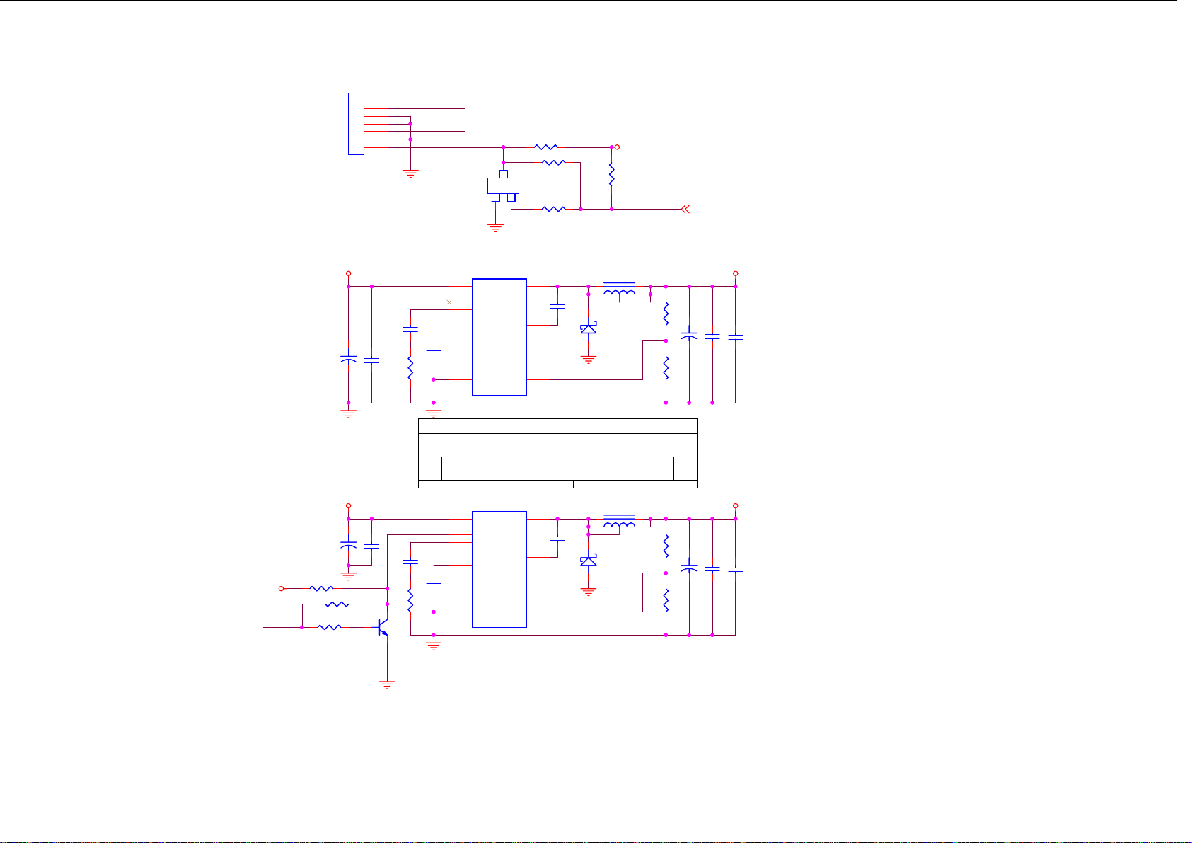
POWER INPUT
CON28
CON28
+12V
+12V
5Vstb
STANDBY
CON7_2.0
CON7_2.0
1
2
3
4
5
6
7
Q34
Q34
23
23
E
E
C
C
SOT
SOT
B
B
132
R337 4.7KR337 4.7K
3904
3904
R338
R338
4.7K
4.7K
R336NCR336
NC
5Vstb
R341
R341
Normal: L
4.7K
4.7K
Standby:H
PW_CTL
PW_CTL 2,8
5Vstb
STANDBY
+12V
+12V
470uF/16V
470uF/16V
R35 4.7KR35 4.7K
R36 4.7KR36 4.7K
R46 NC/4.7KR46 NC/4.7K
CA1
CA1
+
+
470uF/16V
470uF/16V
CA2
CA2
+
+
1
C12
0.1uF
0.1uF
C41
C41
0.1uF
0.1uF
U1
BST
BST
3
1
5
FB
3
1
5
FB
VCC2OUT
7
EN
6
C4
10nFC410nF
R8
7.5KR87.5K
Title
Title
Title
Size Document Number Rev
Size Document Number Rev
Size Document Number Rev
B
B
B
Date: Sheet
Date: Sheet
Date: Sheet
C5
10nFC510nF
R31
R31
Q31
Q31
7.5K
7.5K
NC/3904
NC/3904
2 3
COMP
8
SS
C18
C18
0.1uF
0.1uF
4
GND
MP1430U1MP1430
Power board
Power board
Power board
MST6X89CL <RevCode>
MST6X89CL <RevCode>
MST6X89CL <RevCode>
U3
VCC2OUT
7
EN
6
COMP
8
SS
C42
C42
0.1uF
0.1uF
4
GND
MP1430U3MP1430
C19
C19
10nF
10nF
C43
C43
10nF
10nF
L3
5 4
1 2
D3
1N5822D31N5822
10uHL410uH
D4
1N5822D41N5822
12 12Monday, November 19, 2007
12 12Monday, November 19, 2007
12 12Monday, November 19, 2007
3
10uHL310uH
3
+5V
R4
3.9KR43.9K
CA3
CA3
+
+
470uF/16V
470uF/16V
R7
1.2KR71.2K
of
of
of
L4
54
12
R33
R33
3.9K
3.9K
CA4
CA4
+
+
R32
R32
470uF/16V
470uF/16V
1.2K
1.2K
C382
C382
10uF
10uF
+5V_Pnl
C383
C383
10uF
10uF
C9
0.1uFC90.1uFC12
C10
C10
0.1uF
0.1uF
30
Page 30
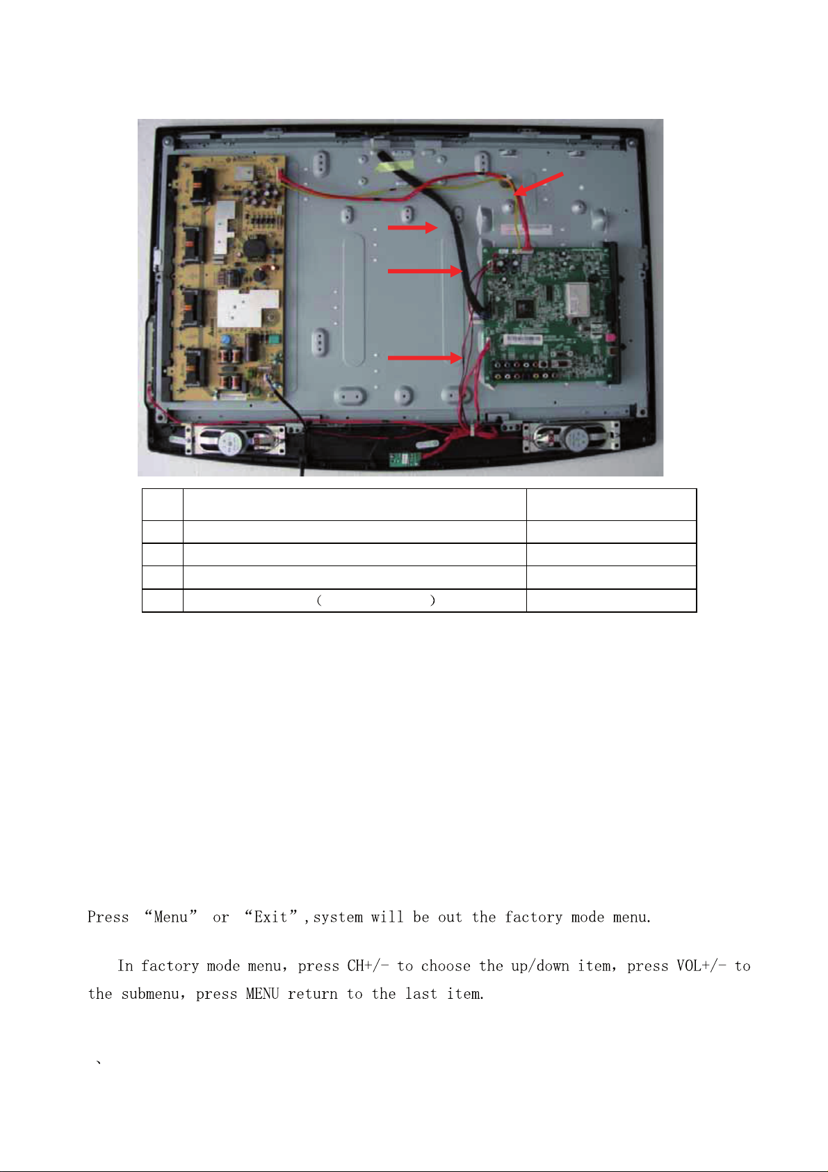
7-2 .Wiring Connection Diagram
2
3
4
NO Name
3 Speaker Wire(Including Speaker)
Connection Wire Keypad&remote
4
eriW SDVL 2
)V5/V21(eriW noitcennoC 1
8. Measurements and Adjustments
1
Parts number
8-1. Service Mode
8-1-1.How to enter into Service Mode
The way to the factory mode menu:
1st, press menu,
2ed, input 8893,
Finished these operations ,system will be into the factory mode menu.
The way to exit the factory mode menu:
Press “Menu”,system will be out the factory mode menu.
8-1-2.How to exit
8-1-3. The default of Factory Mode Menu
MST6X89 FACTORY MENU
1 SOURCE TV/AV1/AV2/YUV/PC/HDMI1/HDMI2
31
Page 31

Press
2、ADC ADJ
Choose the AUTOTUNE to adjust the color of PC/YUV source. Automatically.
16 gray bar in PC source and 75% color bar in YUV source
3、PICTURE MODE
Adjust the Brightness and Contrast in every picture mode.
4、SOUND MODE
Adjust the Bass and Treble in every sound mode.
5、COLOR TEMP
Adjust the Gain and Offset of RGB for every Color Temperature.
6、EEPROM ADJUST
No use in the software.
7、NON LINER
Adjust the linear value of Brightness, Contrast, Definition, Chroma, Volumn, Treble and Bass
8、SSC SETING
No use in the software.
9、DIMMER
No use in the software.
10、OTHET OPTION
PW2STD SAVE :The status is memorizable in AC~ power on time
ON: The status is standby in AC~ power on time
OFF: The status is AutoPowerOn in AC~ power on time
TEST PANEL:No use in the software.
SOUND CARRIER:No use in the software.
FAVOURITE PROG: Switch of Favourite Program
USB: No use in the software。
FINE TUNE:Adjust the ADC value for tuner.
PWM ADJ:Adjust the backlight value of LCD panel.
11、E2P INT :Initialization of software(Restart after the initialization)
12、DLC:Dynamic Light Control for brightness.Testing only!
VOL+/- to choose the Source you want in
factory mode.
9. Trouble shooting
9-1. Simple check
No Picture,no sound
Blank screen
Verify if the television is properly plugged
Verify if the television is properly supplied power
Verify if electricity is available
Verify if correct signals are input
Press INPUT button to change signal input to TV input
Restart the television of power supply is interrupted
32
Page 32
No sound
Press Mute button and verify if Mute mode is set.
Switch to otger channel and verify if the same problem
happens.
Press VOL+ button to see of he problem can be solved.
Poor sound
No picture in some channel
No color for some channel
program(black and white)
Spots with some or all pictures
Horiaontal/vertical bars or
picture shaking
Television out of control
Verufy if sound system is correct .Refer to some chapter for
adjust.
Verify if correct channel is selected.
Adjust the antenna.
Make adjustments by Fine Tune and MANUAL Scan.
Verify if the same problem exists in other channels.
check out of picture and sound system.
Refer to relative instructions in the Manual for color adjust.
Verify if the antennal is correctly connected.
Verify if the antennal is in good condition.
Make fine adjustment of channel.
Check for local interference such as an electrical appliance or
power tool.
Disconnect the television from power supply and 10 seconds
later, connect the television to the power supply. If the problem
still exists, contact authorized after-sales service for technical
assistance.
9-2. Main board failure check
State:No picture
First,check cables which connect with PSU,then check as follows
Check input voltage
voltage: +5VSB→POWER ON(2.6V) →+12V
33
Page 33
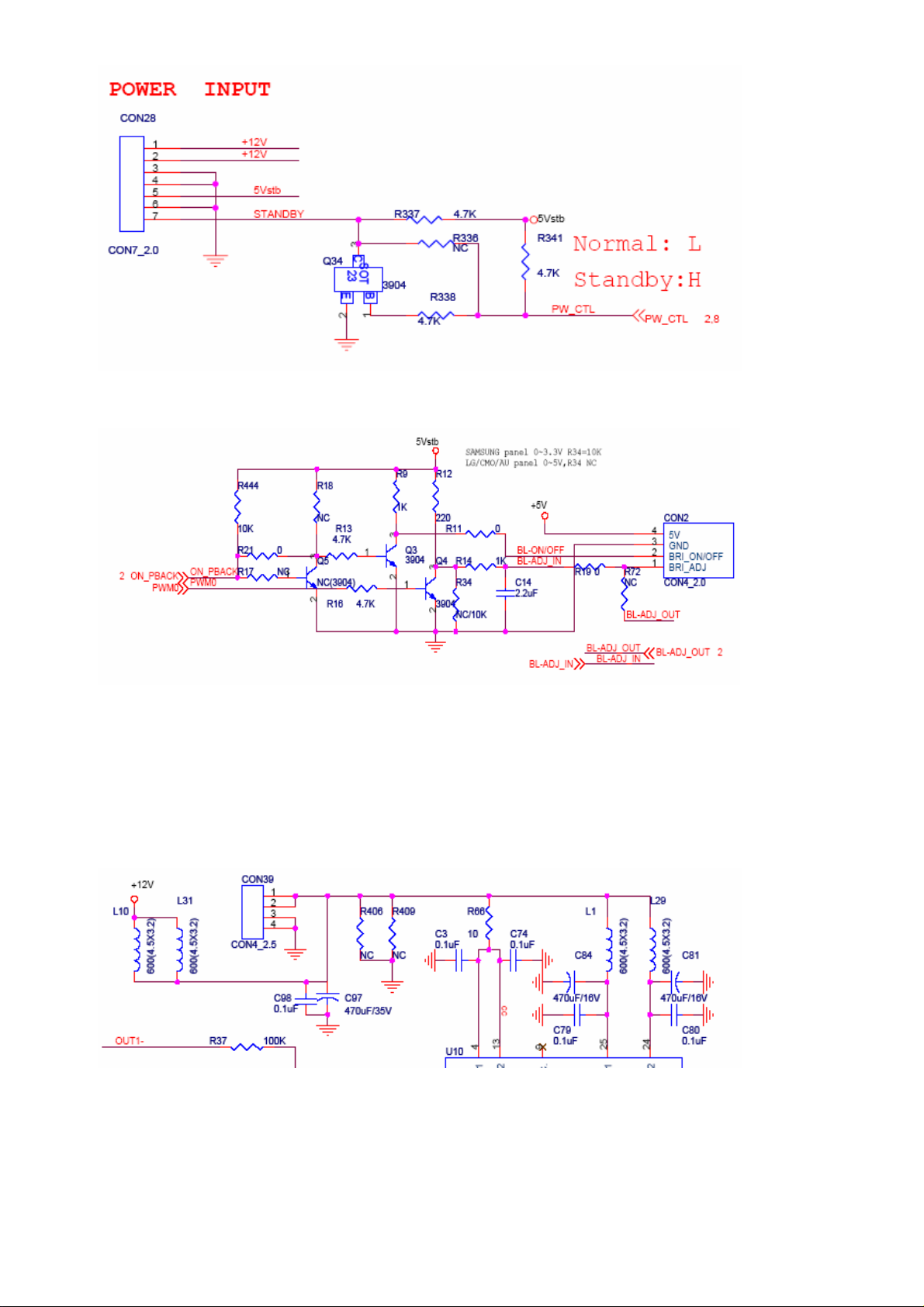
Backlight control CON2
if BRI_ON/OFF(5V) then BACKLIGHT ON
State:No sound
First,check cables which connect with PSU,then check as follows
1) Check input voltage as NO picture
2) Check speaker output
First,check speaker anode(+) and cathode(-),confirm speaker short or not.If short ,replace speaker.
Second,check CNC1 with oscillograph,confirm wave output or not.
Power supply for AMP(U10)-L42T1 16.5V,L47T1 12V
9-3. Pannel failure
Failure Mode
34
Page 34
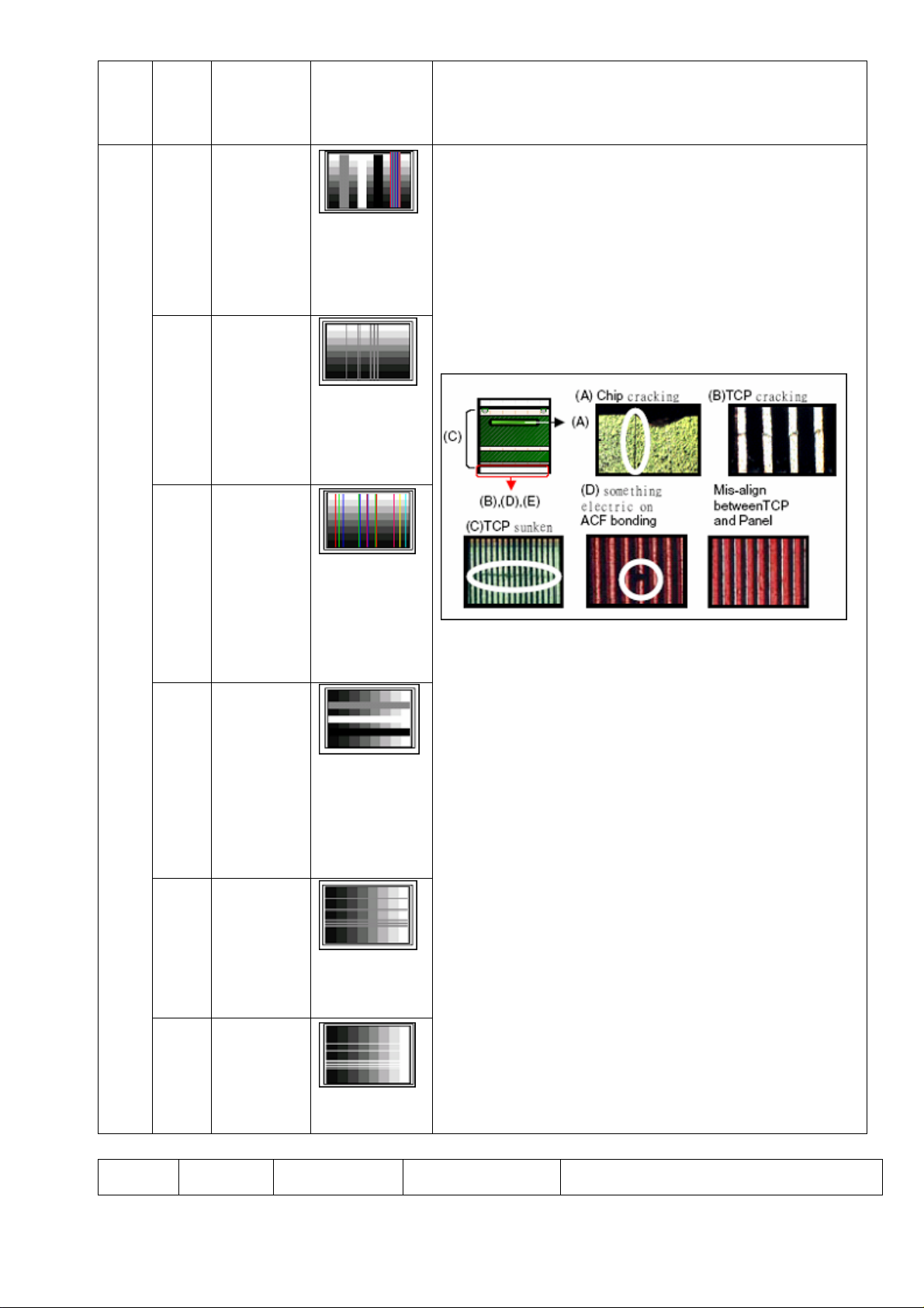
Part Name Description Phenomena Failure cause
Block Defect :TCP cracking or cracking
Dim or L/D :TCP Sunken
:TCP lead cracking
V B/D Vertical bar
:ACF bonding short
:Awful environment and something electric enter into
LCD
:Mis-align between TCP and Panel
:Panel failure
:TCP failure
TCP
V Dim
V L/D
H B/D
Vertal gray
line
Vertical color
line(light or
dark forever)
Horizontal
bar
H Dim
H L/D
Horizontal
gary line
Horizontal
line(light or
dark forever)
Failure Mode
Part Name Description Phenomena Failure cause
35
Page 35
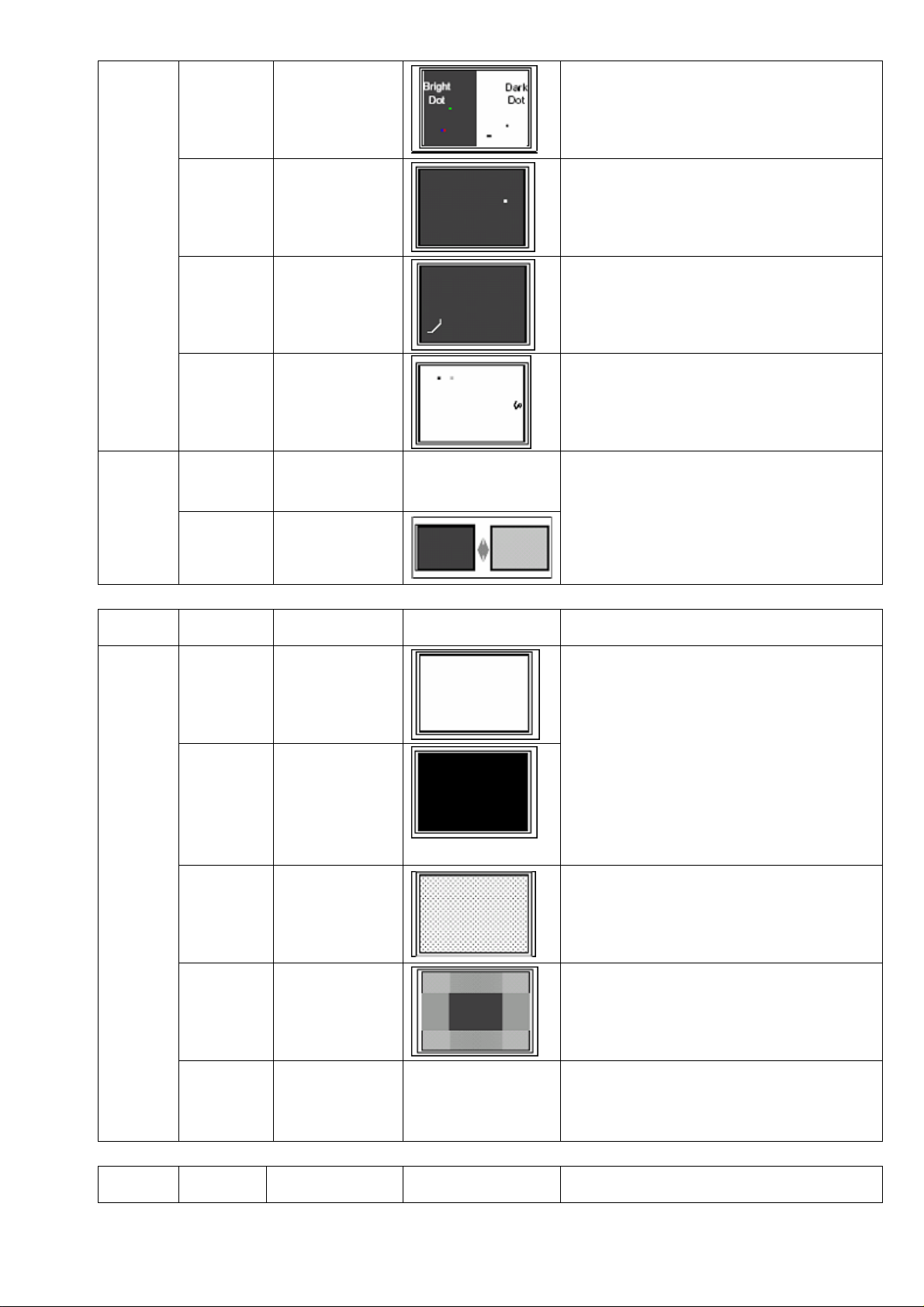
Dot Defect
Bright dot dark
dot in pannel
Incoming Inspection Standard
Panel or
Polarlzer
Polarizer
Bubble
Bladder in
Polarizer
Bladder between Polarizer and top glass
Polarizer
Scratch
Polarizer Scratch
Tine or rigidity arose
F/M inside
Polarizer
Eyewinker inside
Polarizer
Eyewinker inside Polarizer
1. Chip lose action
2. IC ahort or jointiog bad
3. Pannel and vsc connect bad
Circuit
Abnormal
Display
Flashing
Abnormal Display
Bright and dark
display alternately
Failure Mode
Part Name Description Phenomena Failure cause
Circuit
White
Screen
Black
Screen
FIIcker Crosstalk
Abnormal
Color
Abnormal
Color
B/L normal, only
white screen
display
B/L normal, only
Black screen
display
Only color
abormal
Only color
abnormal
Maybe caused by surge current and EDS
LCD Vcom imbalance
Capacitance improper bring crosstalk inside LCD
pannel
1. Chip lose action
2. IC short or jointion bad
3. Pannel and vsc connect bad
Failure Mode
Part Name Description Phenomena Failure cause
36
Page 36
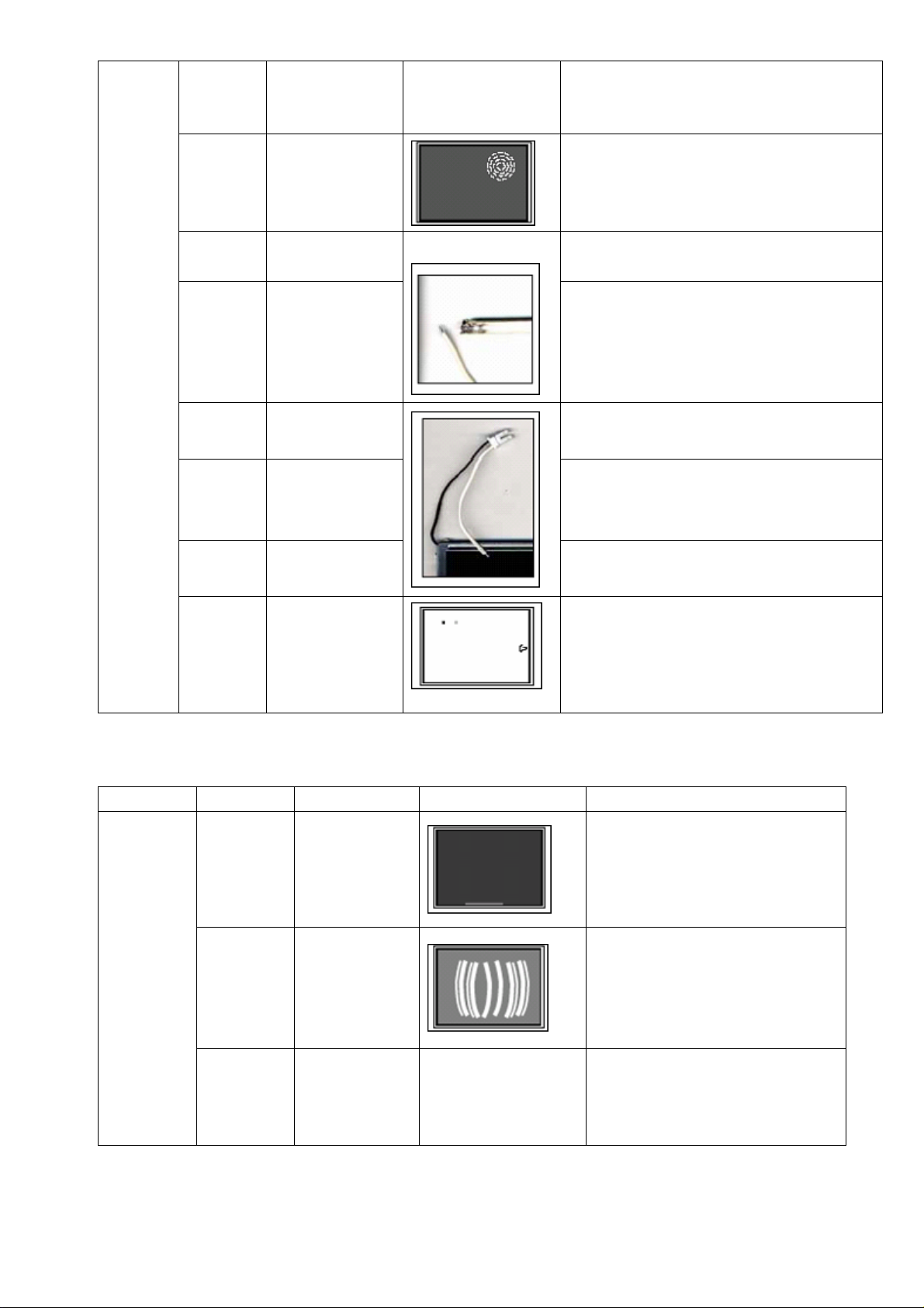
Mechanlcal
Nolse
When turn
panel,appear
cacophony
Caused by Mechanica noise of backlight
unit
Ripple Connectric circle
Causeed by between mechanism and
pannel
B/L off B/L lose action
*Connect badness between wire and
electrode
B/L dark
B/L brightness
darker than normal
B/L wire
damaged
B/L wire
open
B/L shut
down
F/M
B/L wire damaged Operation abnormal or systemic noise
Without backlight Operation abnormal or systemic noise
B/L shutdown in
sometime
F/M in
B/L ,white,balck
Rotundity or
wirelike
*Connect badness
Short between wire and electrode
Short bitween lamp housing and wire, Because
consume power too much
F/M in B/L unit
Failure Mode
Part Name Description Phenomena Failure cause
Brightness at
Mechanlcal
or B/L
Light
leakage
Uniformity
Mount hole
bottom of LCM
brighter than
normal
B/L brightness
asymmetric
Lack screw or
screw damage
B/L unit badness
Sheet in B/L unit is uneven
*Lack screw
Screw damage
37
 Loading...