

Page 1
Global LCD Panel Exchange Center
MODEL NO.: V645HQ1
www.panelook.com
PRODUCT SPECIFICATION
□ Tentative Specification
□ Preliminary Specification
■ Approval Specification
SUFFIX: LS1
Customer:
APPROVED BY SIGNATURE
Name / Title
Note
Please return 1 copy for your confirmation with your
signature and comments.
Approved By Checked By Prepared By
Chao-Chun Chung
Ken Wu
Chloe Chen
Version 2.1 1 Date
The copyright belongs to CHIMEI InnoLux. Any unauthorized use is prohibited
One step solution for LCD / PDP / OLED panel application: Datasheet, inventory and accessory!
ΚΚΚΚ
19 April, 2012
www.panelook.com
Page 2

Global LCD Panel Exchange Center
www.panelook.com
PRODUCT SPECIFICATION
CONTENTS
1. GENERAL DESCRIPTION...................................................................................................................................................5
1.1 OVERVIEW....................................................................................................................................................5
1.2 FEATURES ....................................................................................................................................................5
1.3 APPLICATION................................................................................................................................................5
1.4 GENERAL SPECIFICATIONS ........................................................................................................................5
1.5 MECHANICAL SPECIFICATIONS ..................................................................................................................6
2. ABSOLUTE MAXIMUM RATINGS....................................................................................................................................7
2.1 ABSOLUTE RATINGS OF ENVIRONMENT....................................................................................................7
2.2 PACKAGE STORAGE ....................................................................................................................................8
2.3 ELECTRICAL ABSOLUTE RATINGS..............................................................................................................8
2.3.1 TFT LCD MODULE...............................................................................................................................8
2.3.2 BACKLIGHT UNIT................................................................................................................................8
3. ELECTRICAL CHARACTERISTICS ................................................................................................................................... 9
3.1 TFT LCD MODULE.........................................................................................................................................9
3.2 BACKLIGHT CONNECTOR PIN CONFIGURATION.....................................................................................12
3.2.1 LED LIGHT BAR CHARACTERISTICS (Ta = 25 ± 2 ºC)......................................................................12
3.2.2 CONVERTER CHARACTERISTICS (Ta = 25 ± 2 ºC)..........................................................................12
3.2.3 CONVERTER INTERFACE CHARACTERISTICS...............................................................................14
4. BLOCK DIAGRAM OF INTERFACE................................................................................................................................ 16
4.1 TFT LCD MODULE.......................................................................................................................................16
5. INPUT TERMINAL PIN ASSIGNMENT ..........................................................................................................................17
5.1 TFT LCD Module Input .................................................................................................................................17
5.2 BACKLIGHT UNIT........................................................................................................................................ 20
5.3 CONVERTER UNIT......................................................................................................................................21
5.4 BLOCK DIAGRAM OF INTERFACE .............................................................................................................23
5.5 LVDS INTERFACE .......................................................................................................................................24
5.6 COLOR DATA INPUT ASSIGNMENT............................................................................................................25
6. INTERFACE TIMING......................................................................................................................................................... 26
6. 1 INPUT SIGNAL TIMING SPECIFICATIONS.................................................................................................26
6.2 POWER ON/OFF SEQUENCE.....................................................................................................................32
Version 2.1 2 Date
The copyright belongs to CHIMEI InnoLux. Any unauthorized use is prohibited
One step solution for LCD / PDP / OLED panel application: Datasheet, inventory and accessory!
ΚΚΚΚ
19 April, 2012
www.panelook.com
Page 3
Global LCD Panel Exchange Center
www.panelook.com
PRODUCT SPECIFICATION
7. OPTICAL CHARACTERISTICS ........................................................................................................................................33
7.1 TEST CONDITIONS .....................................................................................................................................33
7.2 OPTICAL SPECIFICATIONS........................................................................................................................34
8. PRECAUTIONS ..................................................................................................................................................................41
8.1 ASSEMBLY AND HANDLING PRECAUTIONS .............................................................................................41
8.2 SAFETY PRECAUTIONS............................................................................................................................. 41
9. DEFINITION OF LABELS..................................................................................................................................................42
9.1 CMI MODULE LABEL...................................................................................................................................42
10. PACKAGING ....................................................................................................................................................................43
10.1 PACKAGING SPECIFICATIONS.................................................................................................................43
10.2 PACKAGING METHOD ..............................................................................................................................43
11. MECHANICAL CHARACTERISTIC ..............................................................................................................................45
Version 2.1 3 Date
The copyright belongs to CHIMEI InnoLux. Any unauthorized use is prohibited
One step solution for LCD / PDP / OLED panel application: Datasheet, inventory and accessory!
ΚΚΚΚ
19 April, 2012
www.panelook.com
Page 4

Global LCD Panel Exchange Center
www.panelook.com
PRODUCT SPECIFICATION
REVISION HISTORY
Version Date Page(New) Section Description
Ver. 2.0 Mar. 05,2012 All All The Approval Specification was first issued.
Ver. 2.1 Apr. 19,2012 P32
6.2 Modify 6.2 POWER ON/OFF SEQUENCE
Version 2.1 4 Date
The copyright belongs to CHIMEI InnoLux. Any unauthorized use is prohibited
One step solution for LCD / PDP / OLED panel application: Datasheet, inventory and accessory!
ΚΚΚΚ
19 April, 2012
www.panelook.com
Page 5
Global LCD Panel Exchange Center
1. GENERAL DESCRIPTION
1.1 OVERVIEW
V645HQ1-LS1 is a 64.5” TFT Liquid Crystal Display module with LED Backlight unit and 2ch LVDS interface. This
module supports 1920 x 1080 Full HDTV format and can display 1.07G colors (8-bit+hi-FRC). The converter
module for backlight is built-in.
1.2 FEATURES
Ё High contrast ratio (5000:1)
Ё Fast response time (4ms)
Ё High color saturation (NTSC 70%)
Ё Full HDTV (1920 x 1080 pixels) resolution, true HDTV format
Ё LVDS (Low Voltage Differential Signaling) interface
Ё Optimized response time for 240 Hz frame rate
www.panelook.com
PRODUCT SPECIFICATION
Ё Ultra wide viewing angle : Super MVA technology
Ё Viewing Angle : 176(H)/176(V) (CR>20)
Ё RoHS compliance
1.3 APPLICATION
Ё Standard Living Room TVs
Ё Public Display Application
Ё Home Theater Application
Ё MFM Application
1.4 GENERAL SPECIFICATIONS
Item Specification Unit Note
Active Area 1428.48 (H) x 803.52 (V) (64.5” diagonal) mm
Bezel Opening Area 1440.6(H) x 814.6(V) mm
Driver Element a-si TFT active matrix - -
Pixel Number 1920 x R.G.B. x 1080 pixel -
Pixel Pitch(Sub Pixel) 0.248 (H) x 0.744 (V) mm -
Pixel Arrangement RGB vertical stripe - -
(1)
Display Colors 1.07G colors (8-bit+hi-FRC) color -
Display Operation Mode Transmissive mode / Normally Black - -
Surface Treatment
Note (1) Please refer to the attached drawings in chapter 11 for more information about the front and back outlines.
Note (2) The spec. of the surface treatment is temporarily for this phase. CMI reserves the rights to change this feature.
Anti-Glare coating Haze<4%
Version 2.1 5 Date
The copyright belongs to CHIMEI InnoLux. Any unauthorized use is prohibited
ΔHardness:3H
ΚΚΚΚ
19 April, 2012
One step solution for LCD / PDP / OLED panel application: Datasheet, inventory and accessory!
- (2)
www.panelook.com
Page 6
Global LCD Panel Exchange Center
1.5 MECHANICAL SPECIFICATIONS
Item Min. Typ. Max. Unit Note
Horizontal (H) 1472.3 1474.1 1475.9 mm (1)
Vertical (V) 849.1 850.6 852.1 mm (1)
Module Size
Depth (D) 34 35 36 mm (2)
Depth (D) 28.8 29.8 30.8 mm (3)
Weight - 29600 - g -
Note (1) Please refer to the attached drawings for more information of front and back outline dimensions.
Note (2) Module Depth is between bezel to T-CON cover.
Note (3) Module Depth is between bezel to converter cover.
www.panelook.com
PRODUCT SPECIFICATION
Version 2.1 6 Date
The copyright belongs to CHIMEI InnoLux. Any unauthorized use is prohibited
One step solution for LCD / PDP / OLED panel application: Datasheet, inventory and accessory!
ΚΚΚΚ
19 April, 2012
www.panelook.com
Page 7
Global LCD Panel Exchange Center
2. ABSOLUTE MAXIMUM RATINGS
2.1 ABSOLUTE RATINGS OF ENVIRONMENT
Item Symbol
Storage Temperature TST -20 +60 ºC (1)
Operating Ambient Temperature TOP 0 50 ºC (1), (2)
Shock (Non-Operating) SNOP - 35 G (3), (5)
Vibration (Non-Operating) VNOP - 1.0 G (4), (5)
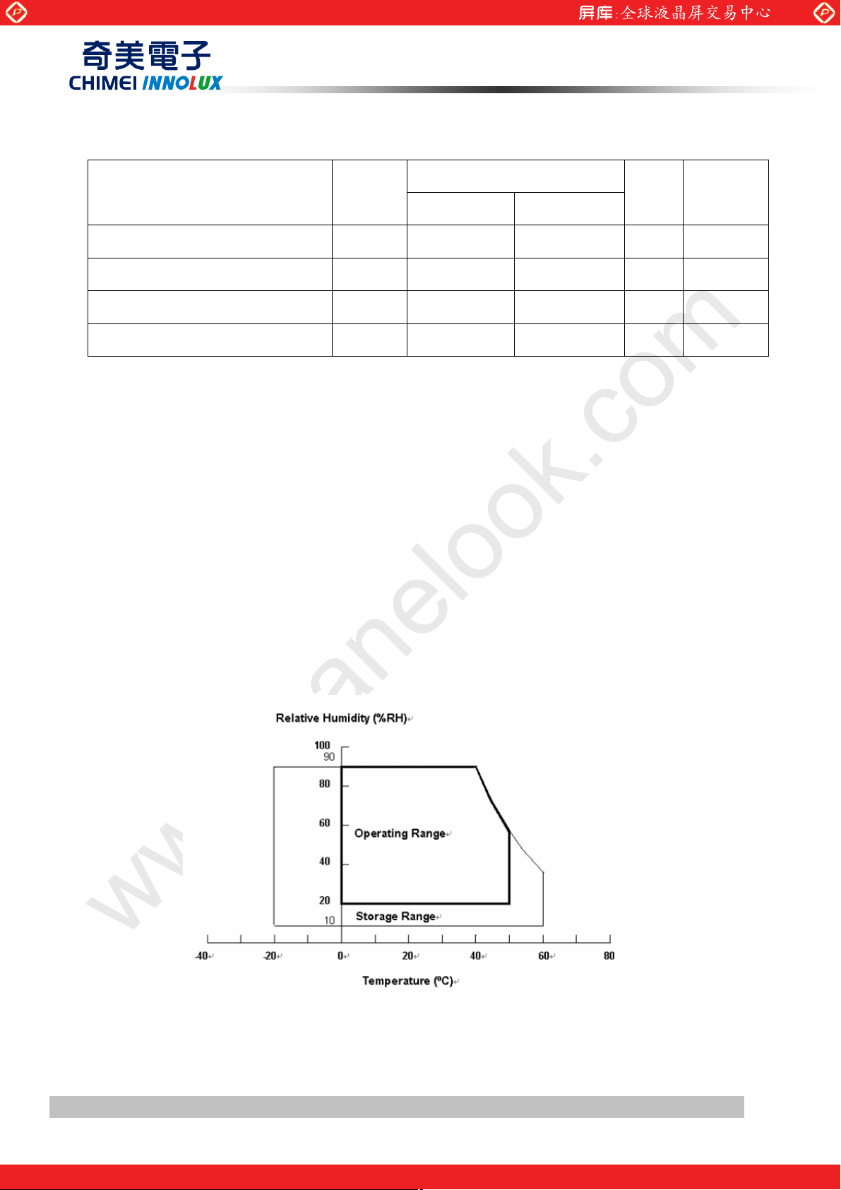
Note (1) Temperature and relative humidity range is shown in the figure below.
www.panelook.com
PRODUCT SPECIFICATION
Value
Unit Note
Min. Max.
(a) 90 %RH Max. (Ta
(b) Wet-bulb temperature should be 39 ºC Max. (Ta > 40 ºC).
(c) No condensation.
Note (2) The maximum operating temperature is based on the test condition that the surface temperature of
display area is less than or equal to 65 ºC with LCD module alone in a temperature controlled chamber.
Thermal management should be considered in final product design to prevent the surface temperature
of display area from being over 65 ºC. The range of operating temperature may degrade in case of
improper thermal management in final product design.
Note (3) 11 ms, half sine wave, 1 time for ± X, ± Y, ± Z.
Note (4) 10 ~ 200 Hz, 10 min, 1 time each X, Y, Z.
Note (5) At testing Vibration and Shock, the fixture in holding the module has to be hard and rigid enough so that
the module would not be twisted or bent by the fixture.
Љ 40 ºC).
Version 2.1 7 Date
The copyright belongs to CHIMEI InnoLux. Any unauthorized use is prohibited
ΚΚΚΚ
19 April, 2012
One step solution for LCD / PDP / OLED panel application: Datasheet, inventory and accessory!
www.panelook.com
Page 8
Global LCD Panel Exchange Center
2.2 PACKAGE STORAGE
When storing modules as spares for a long time, the following precaution is necessary.
(a) Do not leave the module in high temperature, and high humidity for a long time, It is highly recommended to
www.panelook.com
PRODUCT SPECIFICATION
store the module with temperature from 0 to 35
(b) The module shall be stored in dark place. Do not store the TFT-LCD module in direct sunlight or fluorescent
light.
к at normal humidity without condensation.
2.3 ELECTRICAL ABSOLUTE RATINGS
2.3.1 TFT LCD MODULE
Value
Item Symbol
Min. Max.
Power Supply Voltage VCC -0.3 13.5 V
Logic Input Voltage VIN -0.3 3.6 V
2.3.2 BACKLIGHT UNIT
Item Symbol
Light Bar Voltage VW Ta = 25 к - - 60 V
Converter Input Voltage VBL - 0 - 30 V
Control Signal Level - - -0.3 - 6 V
Note (1) Permanent damage to the device may occur if maximum values are exceeded. Function operation
Te st
Condition
Min. Type Max. Unit Note
Unit Note
(1)
RMS
should be restricted to the conditions described under Normal Operating Conditions.
Note (2) No moisture condensation or freezing.
Note (3) The control signals include On/Off Control and External PWM Control
Version 2.1 8 Date
The copyright belongs to CHIMEI InnoLux. Any unauthorized use is prohibited
ΚΚΚΚ
19 April, 2012
One step solution for LCD / PDP / OLED panel application: Datasheet, inventory and accessory!
www.panelook.com
Page 9
Global LCD Panel Exchange Center
3. ELECTRICAL CHARACTERISTICS
3.1 TFT LCD MODULE
(Ta = 25 ± 2 ºC)
Parameter Symbol
Power Supply Voltage VCC 10.8 12 13.2 V (1)
www.panelook.com
PRODUCT SPECIFICATION
Value
Unit Note
Min. Typ. Max.
Rush Current I
White Pattern P
Power consumption
Horizontal Stripe PT
Black Pattern P
White Pattern
Power Supply Current
Horizontal Stripe
Black Pattern
Differential Input High
Threshold Voltage
Differential Input Low
Threshold Voltage
LVDS
interface
Common Input Voltage VCM 1.0 1.2 1.4 V
Differential input voltage
(single-end)
Terminating Resistor R
CMOS
interface
Input High Threshold Voltage VIH 2.7
Input Low Threshold Voltage V
Ё Ё
RUSH
+100
Ё
Ё
Ё
Ё Ё
Ё
T
T
Ё Ё
Ё Ё
Ё Ё
V
LVT H
V
LVTL
| 200
|V
ID
T
0
IL
4.5 A (2)
21 25.2 W
41.64 51.24 W
19.8 23.88 W
1.75 2.1 A
3.47 4.27 A
1.65 1.99 A
Ё Ё
mV
-100 mV
Ё
100
Ё
Ё
600 mV
Ё
ohm
3.3 V
0.7 V
(3)
(3)
(4)
Note (1) The module should be always operated within the above ranges.
Version 2.1 9 Date
ΚΚΚΚ
19 April, 2012
The copyright belongs to CHIMEI InnoLux. Any unauthorized use is prohibited
One step solution for LCD / PDP / OLED panel application: Datasheet, inventory and accessory!
www.panelook.com
Page 10
Global LCD Panel Exchange Center
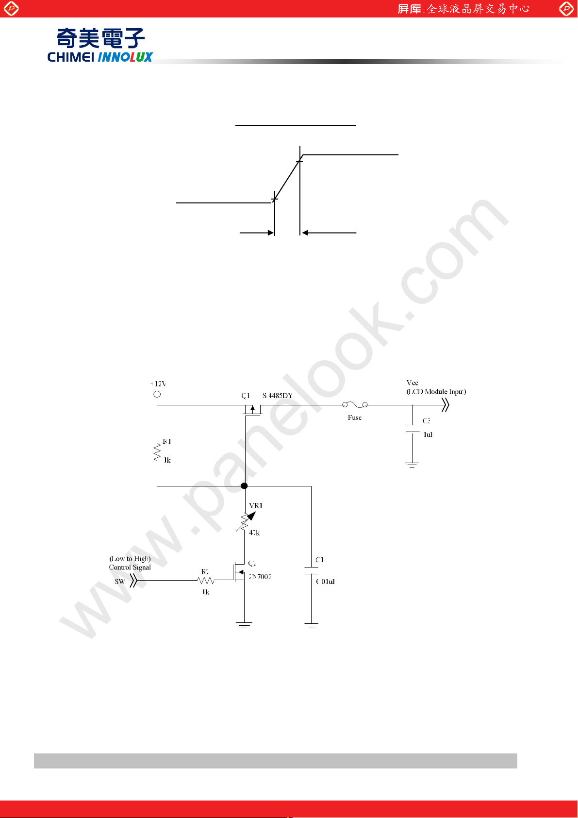
Note (2) Measurement condition:
GND
www.panelook.com
PRODUCT SPECIFICATION
Vcc rising time is 470us
0.9Vcc
0.1Vcc
470us
Vcc
Version 2.1 10 Date
The copyright belongs to CHIMEI InnoLux. Any unauthorized use is prohibited
ΚΚΚΚ
19 April, 2012
One step solution for LCD / PDP / OLED panel application: Datasheet, inventory and accessory!
www.panelook.com
Page 11
Global LCD Panel Exchange Center
Note (3) The specified power supply current is under the conditions at Vcc = 12 V, Ta = 25 ± 2 ºC, fv = 240 Hz,
whereas a power dissipation check pattern below is displayed.
www.panelook.com
PRODUCT SPECIFICATION
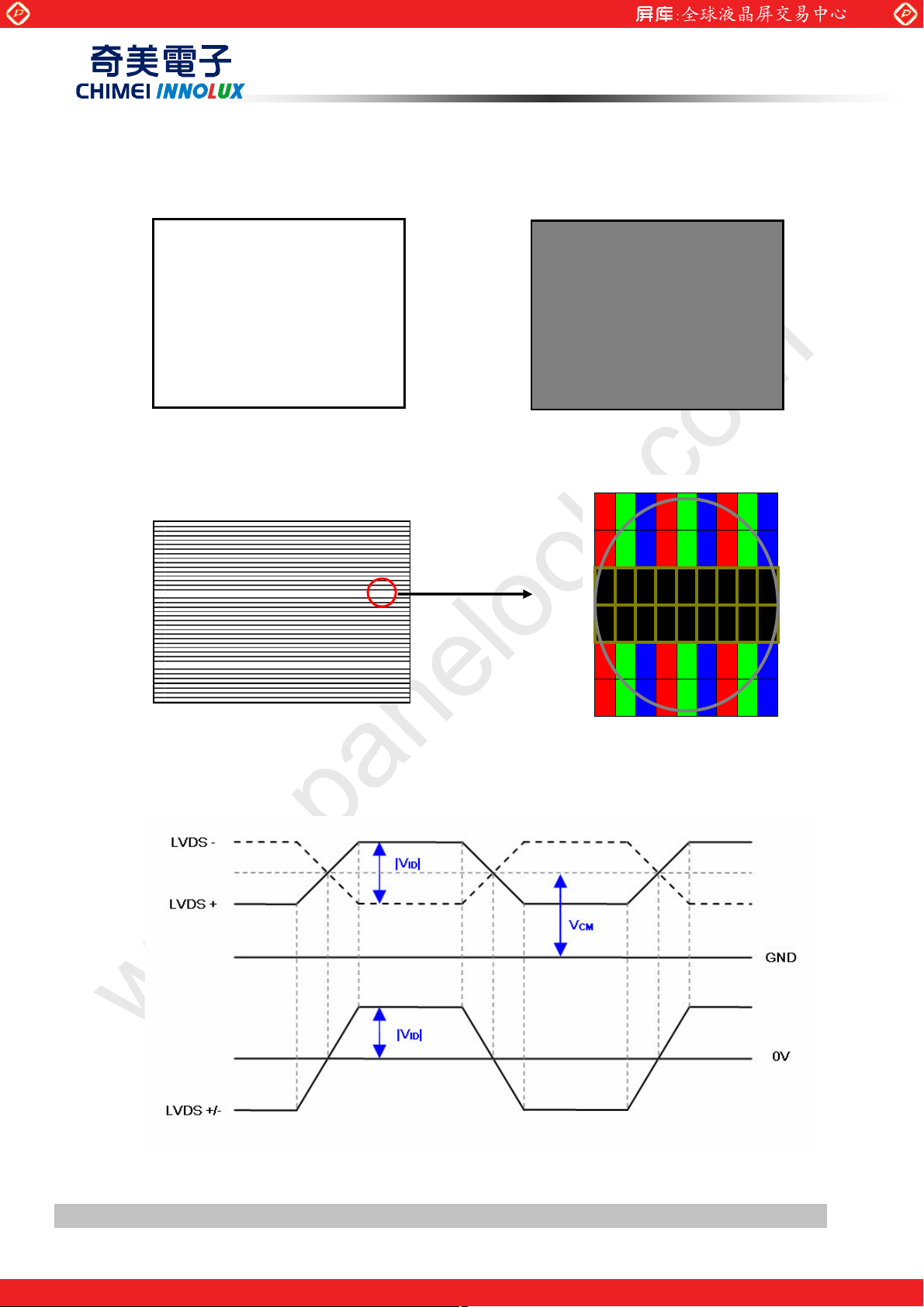
c. Horizontal Pattern
a. White Pattern
Active Area
b. Black Pattern
Active Area
RGBRGBRGB
RGBRGBRGBRGBRGBRGB
RGBRGBRGB
RGBRGBRGBRGBRGBRGB
RGBRGBRGB
RGBRGBRGBRGBRGBRGB
RGBRGBRGB
RGBRGBRGBRGBRGBRGB
Note (4) The LVDS input characteristics are as follows :
RGBRGBRGB
RGBRGBRGBRGBRGBRGB
RGBRGBRGB
RGBRGBRGBRGBRGBRGB
Version 2.1 11 Date
The copyright belongs to CHIMEI InnoLux. Any unauthorized use is prohibited
ΚΚΚΚ
19 April, 2012
One step solution for LCD / PDP / OLED panel application: Datasheet, inventory and accessory!
www.panelook.com
Page 12
Global LCD Panel Exchange Center
www.panelook.com
PRODUCT SPECIFICATION
3.2 BACKLIGHT CONNECTOR PIN CONFIGURATION
3.2.1 LED LIGHT BAR CHARACTERISTICS (Ta = 25 ± 2 ºC)
The backlight unit contains 8pcs light bar.
Parameter Symbol
Unit Note
Min. Typ. Max.
Value
Total Current If
I
One String Current
L(2D)
I
L(3D)
LED Forward Voltage Vf
One String Voltage VW
One String Voltage Variation VϦW
Life time -
4512 4800 5088
141 150 159
TBD 450 TBD
mApeak 3D ENA=ON
2.8 3.2 3.6
30.8 - 39.6
- - 2
30000 - -
mA 32 String
mA
VDC IL =150mA
VDC IL =150mA
V For 1 BLU
Hrs (1)
Note (1) The lifetime is defined as the time which luminance of the LED decays to 50% compared to the
initial value. Operating condition: Continuous operating at Ta = 25±2 , I
к
=150mA
L
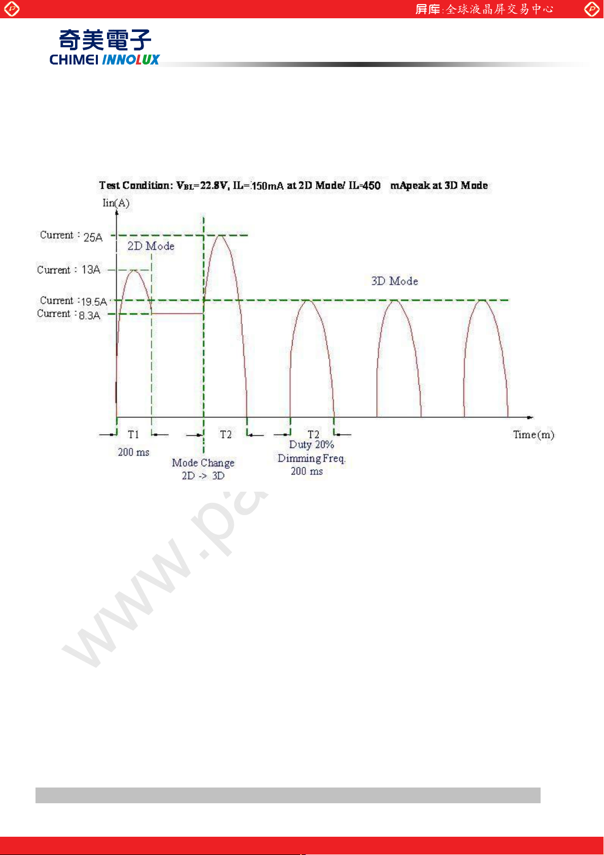
3.2.2 CONVERTER CHARACTERISTICS (Ta = 25 ± 2 ºC)
Value
Parameter Symbol
Unit Note
Min. Typ. Max.
(1), (2)
IL = 150 mA
(1), (2)
IL=450mApeak.
Power Consumption
P
P
BL(2D)
BL(3D)
-
-
188 216.5
185.6 222.7
W
W
Converter Input Voltage VBL 22.8 24.0 25.2 VDC
I
- 7.83 9 A Non Dimming
BL(2D)
Converter Input Current
- 7.7 9.28 A
I
BL(3D)
VBL=22.8V,(IL=typ.)
(3), (6)
=22.8V,(IL=3*typ.)
V
BL
(3), (6)
(5)
(4), (5)
Input Inrush Current
Dimming Frequency
Minimum Duty Ratio
I
-
R(2D)
- - 25 Apeak
I
R(3D)
FB 150 160 170 Hz
DMIN 5 10 - %
- 13
Apeak
Note (1) The power supply capacity should be higher than the total converter power consumption PBL. Since
the pulse width modulation (PWM) mode was applied for backlight dimming, the driving current
changed as PWM duty on and off. The transient response of power supply should be considered
for the changing loading when converter dimming.
Note (2) The measurement condition of Max. value is based on 64.5" backlight unit under input voltage 24V,
average LED current 150mA at 2D Mode (LED current 450mA
at 3D Mode) and lighting 1 hour
peak
later.
Version 2.1 12 Date
ΚΚΚΚ
19 April, 2012
The copyright belongs to CHIMEI InnoLux. Any unauthorized use is prohibited
One step solution for LCD / PDP / OLED panel application: Datasheet, inventory and accessory!
www.panelook.com
Page 13
Global LCD Panel Exchange Center
www.panelook.com
PRODUCT SPECIFICATION
Note (3) For input inrush current measure, the VBL rising time from 10% to 90% is about 30ms.
Note (4) 5% minimum duty ratio is only valid for electrical operation.
Note (5) FB and DMIN are available only at 2D Mode.
Note (6) Below diagram is only for power supply design reference.
Version 2.1 13 Date
The copyright belongs to CHIMEI InnoLux. Any unauthorized use is prohibited
One step solution for LCD / PDP / OLED panel application: Datasheet, inventory and accessory!
ΚΚΚΚ
19 April, 2012
www.panelook.com
Page 14
Global LCD Panel Exchange Center
www.panelook.com
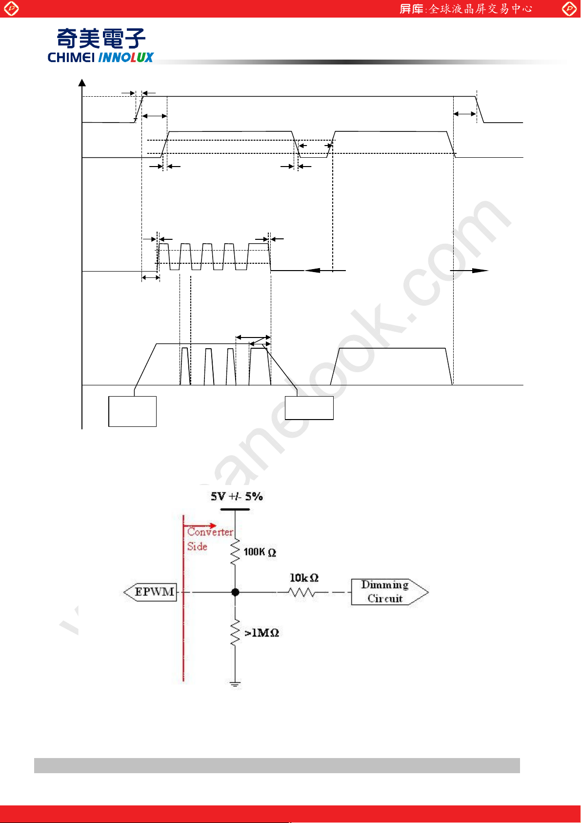
3.2.3 CONVERTER INTERFACE CHARACTERISTICS
PRODUCT SPECIFICATION
Parameter Symbol
ON
On/Off Control Voltage
V
BLON
OFF
External PWM Control
Voltage
External PWM Frequency
HI
LO
V
EPWM
F
EPWM
Error Signal ERR
VBL Rising Time Tr1
Control Signal Rising Time Tr
Control Signal Falling Time Tf
Te st
Condition
Ё
Min. Typ. Max.
2.0
Value
Ё
Unit Note
5.0 V
Ё
Ё
Ё
Ё 150 160 170 Hz Normal mode
Ё Ё Ё Ё Ё
Ё
Ё Ё Ё
Ё Ё Ё
0
2.0
0
30
Ё
Ё
Ё
Ё Ё
0.8 V
5.25 V Duty on
0.8 V Duty off
100 ms
100 ms
(5), (6)
Abnormal: Open
collector
Normal: GND
(4)
ms 10%-90%V
BL
PWM Signal Rising Time T
PWM Signal Falling Time T
PW MR
PW MF
Input Impedance Rin
PWM Delay Time T
PW M
Ton
Ё Ё Ё
Ё Ё Ё
Ё
Ё
Ё
1
100
300
Ё Ё
Ё Ё
Ё Ё
50 us
50 us
MΩ
ms (6)
ms
EPWM, BLON
BLON Delay Time
BLON Off Time T
T
on1
off
Ё
Ё
300
300
Ё Ё
Ё Ё
ms
ms
Note (1) The Dimming signal should be valid before backlight turns on by BLON signal. It is inhibited to
change the external PWM signal during backlight turn on period.
Note (2) The power sequence and control signal timing are shown in the Fig.1. For a certain reason, the
converter has a possibility to be damaged with wrong power sequence and control signal timing.
Note (3) While system is turned ON or OFF, the power sequences must follow as below descriptions:
Turn ON sequence: VBL → PWM signal → BLON
Turn OFF sequence: BLOFF → PWM signal → VBL
Note (4) When converter protective function is triggered, ERR will output open collector status.
(6)
Note (5) The EPWM interface that inserts a pull up resistor to 5V in Max Duty (100%), please refers to Fig.2.
Note (6) EPWM is available only at 2D Mode.
Note(7): [Recommend] EPWM duty ratio is set at 100%(Max. Brightness) in 3D Mode.
Version 2.1 14 Date
ΚΚΚΚ
19 April, 2012
The copyright belongs to CHIMEI InnoLux. Any unauthorized use is prohibited
One step solution for LCD / PDP / OLED panel application: Datasheet, inventory and accessory!
www.panelook.com
Page 15
Global LCD Panel Exchange Center
www.panelook.com
PRODUCT SPECIFICATION
V
V
BL
V
BLON
EPWM
Tr1
%/
9
9
%/
2.0V
0.8V
2.0V
0.8V
Ton
T
Backlight on duration
Tr
Ext. Dimming Function
PWMR
T
PWM
T
Ton1
Tf
PWMF
Floating
0
0
0
Toff
V
W
External
PWM
Period
External
PWM Duty
100%
Fig. 1
Fig. 2
Version 2.1 15 Date
ΚΚΚΚ
19 April, 2012
The copyright belongs to CHIMEI InnoLux. Any unauthorized use is prohibited
One step solution for LCD / PDP / OLED panel application: Datasheet, inventory and accessory!
www.panelook.com
Page 16

Global LCD Panel Exchange Center
)
4. BLOCK DIAGRAM OF INTERFACE
4.1 TFT LCD MODULE
ERX0(+/-)
ERX1(+/-)
ERX2(+/-)
ERX3(+/-)
ERX4(+/-)
ECLK(+/-)
ORX0(+/-)
ORX1(+/-)
ORX2(+/-)
ORX3(+/-)
ORX4(+/-)
OCLK(+/-)
(FI-RE51S-HF (JAE)) or equivalent
INPUT CONNECTOR
Gamma
LR_O
GV_SEL
SELLVDS
Blanking
Bit select
MEMC demo
L/R
SCL
SDA
LD_EN
www.panelook.com
PRODUCT SPECIFICATION
TIMING
CONTROLLER
circuit
DC/DC CONVERTER
& REFERENCE VOLTAGE
GENERATOR
SCAN DRIVER
TFT LCD PANEL
(1920x3x1080)
Data Driver(mini-LVDS
VIN
GND
VLED
PGND
BLON
ERR
E_PWM
LD-Edge Board
CN: CI0114M1HR0-LA
(Cvilux) or equivalent
CN: CI0112M1HR0-LA
(Cvilux) or equivalent
CN:196357-15041-3
(P-TWO) or equivalent
CN : 196357-15041-3 (P-TWO) or equivalent
BACKLIGHT
UNIT
Version 2.1 16 Date
ΚΚΚΚ
The copyright belongs to CHIMEI InnoLux. Any unauthorized use is prohibited
One step solution for LCD / PDP / OLED panel application: Datasheet, inventory and accessory!
19 April, 2012
www.panelook.com
Page 17

Global LCD Panel Exchange Center
www.panelook.com
5. INPUT TERMINAL PIN ASSIGNMENT
5.1 TFT LCD Module Input
CNF1 Connector Part No.: P-TWO 187059-51221 or equivalent.
Pin Name Description Note
1 NC No Connection (3)
2SCL
3SDA
4 NC No Connection
5
L/R_O Output signal for Left Right Glasses control
6 GV_SEL
7 SELLVDS Input signal for LVDS Data Format Selection (4)
8
Blanking Blanking enable
9
Bit select 8bit/10bit selection
10
MEMC demo MEMC demo mode enable
11 GND Ground
12 ORX0- 1st pixel Negative LVDS differential data input. Channel 0
13 ORX0+ 1st pixel Positive LVDS differential data input. Channel 0
14 ORX1- 1st pixel Negative LVDS differential data input. Channel 1
15 ORX1+ 1st pixel Positive LVDS differential data input. Channel 1
16 ORX2- 1st pixel Negative LVDS differential data input. Channel 2
17 ORX2+ 1st pixel Positive LVDS differential data input. Channel 2
18 GND Ground
19 OCLK- 1st pixel Negative LVDS differential clock input.
20 OCLK+ 1st pixel Positive LVDS differential clock input
21 GND Ground
22 ORX3- 1st pixel Negative LVDS differential data input. Channel 3
23 ORX3+ 1st pixel Positive LVDS differential data input. Channel 3
24 ORX4- 1st pixel Negative LVDS differential data input. Channel 4
25 ORX4+ 1st pixel Positive LVDS differential data input. Channel 4
26 NC No Connection
27 L/R Input signal for Left Right synchronous signal
28 ERX0- 2nd pixel Negative LVDS differential data input. Channel 0
29 ERX0+ 2nd pixel Positive LVDS differential data input. Channel 0
30 ERX1- 2nd pixel Negative LVDS differential data input. Channel 1
31 ERX1+ 2nd pixel Positive LVDS differential data input. Channel 1
32 ERX2- 2nd pixel Negative LVDS differential data input. Channel 2
33 ERX2+ 2nd pixel Positive LVDS differential data input. Channel 2
34 GND Ground
35 ECLK- 2nd pixel Negative LVDS differential clock input.
36 ECLK+ 2nd pixel Positive LVDS differential clock input
37 GND Ground
38 ERX3- 2nd pixel Negative LVDS differential data input. Channel 3
39 ERX3+ 2nd pixel Positive LVDS differential data input. Channel 3
40 ERX4- 2nd pixel Negative LVDS differential data input. Channel 4
41 ERX4+ 2nd pixel Positive LVDS differential data input. Channel 4
I2C Serial Clock (for 3D format selection function)
I2C Serial Data (for 3D format selection function)
Graphic/Video mode selection
PRODUCT SPECIFICATION
(3)
(5)
(6)
(7)
(1)
(1)
(1)
(1)
(1)
(1)
Version 2.1 17 Date
The copyright belongs to CHIMEI InnoLux. Any unauthorized use is prohibited
ΚΚΚΚ
19 April, 2012
One step solution for LCD / PDP / OLED panel application: Datasheet, inventory and accessory!
www.panelook.com
Page 18

Global LCD Panel Exchange Center
42
LD_EN Input signal for Local Dimming Enable
43 NC No Connection
44 GND Ground
45 GND Ground
46 GND Ground
47 NC No Connection
48 VCC +12V power supply
49 VCC +12V power supply
50 VCC +12V power supply
51 VCC +12V power supply
Note (1) Two pixel data send into the module for every clock cycle. The first pixel of the frame is odd pixel and the
second pixel is even pixel
www.panelook.com
PRODUCT SPECIFICATION
(8)
Note (2) LVDS connector pin order defined as follows
Note (3) G/V select. (Default : Graphic mode)
L= Connect to GND, H=Connect to +3.3V or Open
G/V select Note
L Video mode
H or Open Graphic mode
Note (4) SELLVDS. (Default : VESA)
L= Connect to GND or Open, H=Connect to +3.3V
SELLVDS Note
H or Open VESA
L JEIDA
Version 2.1 18 Date
The copyright belongs to CHIMEI InnoLux. Any unauthorized use is prohibited
ΚΚΚΚ
19 April, 2012
One step solution for LCD / PDP / OLED panel application: Datasheet, inventory and accessory!
www.panelook.com
Page 19

Global LCD Panel Exchange Center
Note (5) Blanking. (Default : Disable)
L= Connect to GND or Open, H=Connect to +3.3V
Blanking Note
L or Open Disable
H Enable
Note (6) Bit select. (Default : 10bit)
L= Connect to GND or Open, H=Connect to +3.3V
Bit select Note
L or Open 10bit
H 8bit
www.panelook.com
PRODUCT SPECIFICATION
Note (7) MEMC demo. (Default : Disable)
L= Connect to GND or Open, H=Connect to +3.3V
MEMC demo Note
L or Open Disable
H Enable
Note (8) LD_EN. (Default : Disable)
L= Connect to GND or Open, H=Connect to +3.3V
LD_EN Note
L or Open Disable
H Enable
Version 2.1 19 Date
The copyright belongs to CHIMEI InnoLux. Any unauthorized use is prohibited
ΚΚΚΚ
19 April, 2012
One step solution for LCD / PDP / OLED panel application: Datasheet, inventory and accessory!
www.panelook.com
Page 20

Global LCD Panel Exchange Center
5.2 BACKLIGHT UNIT
The pin configuration for the housing and leader wire is shown in the table below.
www.panelook.com
PRODUCT SPECIFICATION
ΕCN6: 196357-15041-3 (P-TWO)
CN3
Pin No. Symbol Feature
1 NC No Connection
2 LED1 Negative of LED String
3 LED2 Negative of LED String
4 LED3 Negative of LED String
5 LED4 Negative of LED String
6 LED5 Negative of LED String
7 LED6 Negative of LED String
8 LED7 Negative of LED String
9 LED8 Negative of LED String
10 NC No Connection
11 NC No Connection
12 VCC_LED Positive of LED String
13 VCC_LED Positive of LED String
14 VCC_LED Positive of LED String
15 VCC_LED Positive of LED String
ΕCN5: 196357-15041-3 (P-TWO)
CN4
Pin No. Symbol Feature
1 VCC_LED Positive of LED String
2 VCC_LED Positive of LED String
3 VCC_LED Positive of LED String
4 VCC_LED Positive of LED String
5 NC No Connection
6 NC No Connection
7 LED8 Negative of LED String
8 LED7 Negative of LED String
9 LED6 Negative of LED String
10 LED5 Negative of LED String
11 LED4 Negative of LED String
12 LED3 Negative of LED String
13 LED2 Negative of LED String
14 LED1 Negative of LED String
15 NC Negative of LED String
Version 2.1 20 Date
The copyright belongs to CHIMEI InnoLux. Any unauthorized use is prohibited
ΚΚΚΚ
19 April, 2012
One step solution for LCD / PDP / OLED panel application: Datasheet, inventory and accessory!
www.panelook.com
Page 21

Global LCD Panel Exchange Center
5.3 CONVERTER UNIT
www.panelook.com
PRODUCT SPECIFICATION
CN1: CI0114M1HR0-LA (Cvilux)
Pin № Symbol Feature
1
2
3
4
5
6
7
8
9
10
11 ERR
12 BLON
13 NC
14 E_PWM
Notice: 1. If Pin14 is open, E_PWM is 100% duty.
VLED +24V
GND GND
Normal (GND)
Abnormal (Open collector)
BL ON/OFF
NC
External PWM Control
Version 2.1 21 Date
The copyright belongs to CHIMEI InnoLux. Any unauthorized use is prohibited
ΚΚΚΚ
19 April, 2012
One step solution for LCD / PDP / OLED panel application: Datasheet, inventory and accessory!
www.panelook.com
Page 22

Global LCD Panel Exchange Center
www.panelook.com
PRODUCT SPECIFICATION
CN2: CI0112M1HR0-LA (Cvilux)
Pin № Symbol Feature
1
2
3
4
5
6
7
8
9
10
11 NC No Connection
12 NC No Connection
VLED +24V
GND GND
Version 2.1 22 Date
The copyright belongs to CHIMEI InnoLux. Any unauthorized use is prohibited
ΚΚΚΚ
19 April, 2012
One step solution for LCD / PDP / OLED panel application: Datasheet, inventory and accessory!
www.panelook.com
Page 23

Global LCD Panel Exchange Center
Ө
Ө
Ө
5.4 BLOCK DIAGRAM OF INTERFACE
www.panelook.com
PRODUCT SPECIFICATION
CNF1
ER0-ER9
EG0-EG9
EB0-EB9
OR0-OR9
OG0-OG9
OB0-OB9
Host
Graphics
Controller
ERx0+
ERx1+
ERx2+
ERx3+
ERx4+
ECLK+
ECLK-
ORx0
ORx1
ORx1-
ORx2
ORx3
ORx4
RxOUT
100
Ө
100
100
100
100
100
100
100
100
100
100
100
100pF
Ө
Ө
100pF
Ө
Ө
100pF
Ө
Ө
100pF
Ө
100pF
Ө
Ө
100pF
Ө
ER0-ER9
-
EB0-EB9
DE
OR0-OR9
OG0-OG9
OB0-OB9
DCLK
-
-
-
-
-
Timing
100
100
100
100
100
100
100
100
100
100pF
Ө
Ө
100pF
Ө
Ө
100pF
Ө
Ө
100pF
Ө
100pF
Ө
-
-
-
-
Controller
OCLK+
100
Ө
100pF
OCLK-
100
LVDS Transmitter
LVDS Re ceiver
THC63LVDM83A
(LVDF83A)
Version 2.1 23 Date
The copyright belongs to CHIMEI InnoLux. Any unauthorized use is prohibited
One step solution for LCD / PDP / OLED panel application: Datasheet, inventory and accessory!
ΚΚΚΚ
19 April, 2012
www.panelook.com
Page 24

Global LCD Panel Exchange Center
5.5 LVDS INTERFACE
JEIDA Format : SELLVDS = L
VESA Format : SELLVDS = H or Open
www.panelook.com
PRODUCT SPECIFICATION
R0~R9: Pixel R Data (9; MSB, 0; LSB)
G0~G9: Pixel G Data (9; MSB, 0; LSB)
B0~B9: Pixel B Data (9; MSB, 0; LSB)
DE : Data enable signal
DCLK : Data clock signal
Notes: (1) RSVD (reserved) pins on the transmitter shall be “H” or “L”.
Version 2.1 24 Date
The copyright belongs to CHIMEI InnoLux. Any unauthorized use is prohibited
One step solution for LCD / PDP / OLED panel application: Datasheet, inventory and accessory!
ΚΚΚΚ
19 April, 2012
www.panelook.com
Page 25

Global LCD Panel Exchange Center
5.6 COLOR DATA INPUT ASSIGNMENT
The brightness of each primary color (red, green and blue) is based on the 10-bit gray scale data input for the
color. The higher the binary input the brighter the color. The table below provides the assignment of color versus
data input.
Color
R9 R8 R7 R6 R5 R4 R3 R2 R1 R0 G9 G8 G7 G6 G5 G4 G3 G2 G1 G0 B9 B8 B7 B6 B5 B4 B3 B2 B1 B0
Basic
Colors
Gray
Scale
Of
Red
Gray
Scale
Of
Green
Gray
Scale
Of
Blue
Black
Red
Green
Blue
Cyan
Magenta
Yel lo w
White
Red (0) / Dark
Red (1)
Red (2)
:
:
Red (1021)
Red (1022)
Red (1023)
Green (0) / Dark
Green (1)
Green (2)
:
:
Green (1021)
Green (1022)
Green (1023)
Blue (0) / Dark
Blue (1)
Blue (2)
:
:
Blue (1021)
Blue (1022)
Blue (1023)
0
0
0
1
0
0
0
1
1
1
0
0
0
1
1
1
0
0
0
:
:
0
0
0
0
0
0
:
:
0
0
0
0
1
1
1
0
0
0
0
0
0
0
0
0
1
1
1
1
1
1
1
1
1
0
0
0
0
0
0
0
0
0
:
:
:
:
1
1
1
1
1
1
1
1
1
0
0
0
0
0
0
0
0
0
:
:
:
:
:
:
0
0
0
0
0
0
0
0
0
0
0
0
0
0
0
0
0
0
:
:
:
:
:
:
0
0
0
0
0
0
0
0
0
www.panelook.com
PRODUCT SPECIFICATION
Data Signal
Red Green Blue
0
0
0
0
0
0
0
0
0
0
0
0
0
0
0
0
0
0
0
0
0
0
0
0
0
1
1
1
1
1
1
0
0
0
0
0
0
0
0
0
0
0
0
0
0
0
0
0
0
0
0
0
0
1
1
1
1
1
1
1
1
1
1
0
0
0
0
0
0
0
0
0
0
0
0
0
0
0
0
0
0
0
0
0
0
0
0
0
1
1
1
1
1
1
1
1
1
1
1
1
1
0
0
0
0
1
1
1
1
1
1
1
1
1
1
1
1
0
0
0
0
0
0
0
0
:
:
:
:
1
1
1
1
1
1
0
0
0
0
0
0
:
:
:
:
0
0
0
0
0
0
0
0
0
0
0
0
:
:
:
:
0
0
0
0
0
0
0
0
0
0
0
0
1
:
:
:
:
:
:
1
1
0
1
1
1
1
1
1
0
0
0
0
0
0
0
0
0
:
:
:
:
:
:
0
0
0
0
0
0
0
0
0
0
0
0
0
0
0
0
0
0
:
:
:
:
:
:
0
0
0
0
0
0
0
0
0
1
1
1
1
0
0
0
1
0
0
0
0
0
:
:
:
:
:
:
1
0
0
0
0
0
1
0
0
0
0
0
0
0
0
0
0
0
:
:
:
:
:
:
0
1
1
0
1
1
0
1
1
0
0
0
0
0
0
0
0
0
:
:
:
:
:
:
0
0
0
0
0
0
0
0
0
0
1
1
1
1
1
1
0
0
0
0
0
0
0
0
0
:
:
:
:
:
:
0
0
0
0
0
0
0
0
0
0
0
0
0
0
0
0
0
0
:
:
:
:
:
:
1
1
1
1
1
1
1
1
1
0
0
0
0
0
0
0
0
0
:
:
:
:
:
:
0
0
0
0
0
0
0
0
0
1
0
0
0
1
1
1
1
1
1
0
0
0
0
0
0
0
0
0
:
:
:
:
:
:
0
0
0
0
0
0
0
0
0
0
0
0
0
0
0
0
0
0
:
:
:
:
:
:
1
1
1
1
1
1
1
1
1
0
0
0
0
0
0
0
0
0
:
:
:
:
:
:
0
0
0
0
0
0
0
0
0
1
1
1
1
0
0
1
1
1
0
1
1
1
0
0
0
0
0
0
0
0
0
:
:
:
:
:
;
0
0
0
0
0
0
0
0
0
0
0
0
1
0
0
0
0
1
:
:
:
:
:
:
0
1
0
1
0
0
1
1
0
0
0
0
0
0
0
0
0
0
:
:
:
:
:
:
0
0
1
0
0
1
0
0
1
0
1
1
1
1
1
1
1
1
1
0
0
0
1
1
1
0
0
0
0
0
0
0
0
0
:
:
:
:
:
:
0
0
0
0
0
0
0
0
0
0
0
0
0
0
0
0
0
0
:
:
:
:
:
:
0
0
0
0
0
0
0
0
0
0
0
0
0
0
0
0
0
0
:
:
:
:
:
:
1
1
1
1
1
1
1
1
1
0
0
0
0
1
1
1
1
1
1
1
1
1
0
0
0
1
1
1
0
0
0
0
0
0
0
0
0
:
:
:
:
:
:
0
0
0
0
0
0
0
0
0
0
0
0
0
0
0
0
0
0
:
:
:
:
:
:
0
0
0
0
0
0
0
0
0
0
0
0
0
0
0
0
0
0
:
:
:
:
:
:
1
1
1
1
1
1
1
1
1
0
0
0
0
0
0
0
1
1
1
1
1
1
1
1
1
0
0
0
1
1
1
0
0
0
0
0
0
0
0
0
:
:
:
:
:
:
0
0
0
0
0
0
0
0
0
0
0
0
0
0
0
0
0
0
:
:
:
:
:
:
0
0
0
0
0
0
0
0
0
0
0
0
0
0
1
0
1
0
:
:
:
:
:
:
1
0
1
1
1
0
1
1
1
Note (1) 0: Low Level Voltage, 1: High Level Voltage
Version 2.1 25 Date
ΚΚΚΚ
19 April, 2012
The copyright belongs to CHIMEI InnoLux. Any unauthorized use is prohibited
One step solution for LCD / PDP / OLED panel application: Datasheet, inventory and accessory!
www.panelook.com
Page 26

Global LCD Panel Exchange Center
6. INTERFACE TIMING
6. 1 INPUT SIGNAL TIMING SPECIFICATIONS
(Ta = 25 ± 2 ºC)
The input signal timing specifications are shown as the following table and timing diagram in the 2D mode.
Signal Item Symbol Min. Typ. Max. Unit Note
F
(=1/TC)
clkin_mod
F
F
LVDS
Receiver
Clock
Frequency
Input cycle to
cycle jitter
Spread spectrum
modulation range
Spread spectrum
modulation frequency
www.panelook.com
PRODUCT SPECIFICATION
clkin
SSM
T
rcl
68 75 79 MHz
Ё Ё
F
-3%
clkin
Ё Ё
Ё
200 ps (2)
F
+3% MHz (3)
clkin
150 KHz (4)
LVDS
Receiver
Data
Receiver Skew
Margin
T
RSKM
-400
Ё
400 ps (5)
Version 2.1 26 Date
ΚΚΚΚ
19 April, 2012
The copyright belongs to CHIMEI InnoLux. Any unauthorized use is prohibited
One step solution for LCD / PDP / OLED panel application: Datasheet, inventory and accessory!
www.panelook.com
Page 27

Global LCD Panel Exchange Center
6.1.1 Timing spec for Frame Rate = 50Hz
Signal Item Symbol Min. Typ. Max. Unit Note
Frame rate 2D mode Fr5 47 50 53 Hz
Total Tv 1115 1350 1395 Th Tv=Tvd+Tvb
www.panelook.com
PRODUCT SPECIFICATION
Display Tvd 1080 Th
Vertical
Active
Display
Term
2D Mode
Horizontal
Active
Display
Term
Blank Tvb 35 270 315 Th
Front porch Tvfp 2
Back porch Tvbp 4
Vsync Tvswid 1
Total Th 1040 1100 1340 Tc Th=Thd+Thb
Display Thd 960 Tc
Blank Thb 84 140 380 Tc
Front porch Thfp 8
Back porch Thbp 20
Hsync Thswid 8
Ё Ё
Ё Ё
Ё Ё
Ё Ё
Ё Ё
Ё Ё
Th
Th
Th
Tc
Tc
Tc
Ё
Ё
(6)
Ё
Ё
(6)
Version 2.1 27 Date
The copyright belongs to CHIMEI InnoLux. Any unauthorized use is prohibited
ΚΚΚΚ
19 April, 2012
One step solution for LCD / PDP / OLED panel application: Datasheet, inventory and accessory!
www.panelook.com
Page 28

Global LCD Panel Exchange Center
6.1.2 Timing spec for Frame Rate = 60Hz
Signal Item Symbol Min. Typ. Max. Unit Note
2D mode Fr6 57 60 63 Hz
Frame rate
3D mode F
Total Tv 1115 1125 1395 Th Tv=Tvd+Tvb
www.panelook.com
PRODUCT SPECIFICATION
60 Hz
r6
Vertical
Active
Display
Term
2D Mode
3D Mdoe
Display Tvd 1080 Th
Blank Tvb 35 45 315 Th
Front porch Tvfp 2
Back porch Tvbp 4
Vsync Tvswid 1
Total Tv 1125 Th
Display Tvd 1080 Th
Blank Tvb 45 Th
Front porch Tvfp 2
Back porch Tvbp 4
Vsync Tvswid 1
Total Th 1040 1100 1340 Tc Th=Thd+Thb
Display Thd 960 960 960 Tc
Ё Ё
Ё Ё
Ё Ё
Ё Ё Ё
Ё Ё Ё
Ё Ё Ё
Th
Th
Th
Ё
Ё
(6)
Ё
Ё
Ё
(6)
Ё
Blank Thb 84 140 380 Tc
2D Mode
Ё Ё
Ё Ё
Ё Ё
Ё Ё
Ё Ё
Ё Ё
Horizontal
Active
Display
Term
Front porch Thfp 8
Back porch Thbp 20
Hsync Thswid 8
Total Th 1040 1100 1340 Tc Th=Thd+Thb
Display Thd 960 960 960 Tc
Blank Thb 84 140 380 Tc
3D Mdoe
Front porch Thfp 8
Back porch Thbp 20
Hsync Thswid 8
Version 2.1 28 Date
The copyright belongs to CHIMEI InnoLux. Any unauthorized use is prohibited
Ё
Tc
Tc
Tc
Tc
Tc
Tc
ΚΚΚΚ
19 April, 2012
(6)
Ё
Ё
(6)
One step solution for LCD / PDP / OLED panel application: Datasheet, inventory and accessory!
www.panelook.com
Page 29

Global LCD Panel Exchange Center
6.1.3 Timing spec for 3D 720P
Signal Item Symbol Min. Typ. Max. Unit Note
Total Tv 750 800 860 Th Tv=Tvd+Tvb
www.panelook.com
PRODUCT SPECIFICATION
Display Tvd 720 Th
Vertical
Active
Display
Term
Horizontal
Active
Display
Term
Note (1) Please make sure the range of pixel clock has follow the below equation
3D Mode
3D Mode
Blank Tvb 20 - - Th
Front porch Tvfp 2 Th
Back porch Tvbp 4 Th
Vsync Tvswid 1 Th
Total Th 1600 Tc Th=Thd+Thb
Display Thd 640 640 640 Tc
Blank Thb 120 - - Tc
Front porch Thfp 24
Back porch Thbp 20
Hsync Thswid 8
Ё Ё
Ё Ё
Ё Ё
Κ
Tc
Tc
Tc
Ё
Ё
(6)
Ё
Ё
(6)
Fclkin(max) F
Fr5 Tv Th F
ѼѼЊclkin(min)
Note (2) The input clock cycle-to-cycle jitter is defined as below figures. Trcl = I T
Њ r6 Tv ThѼѼ
– TI
1
Version 2.1 29 Date
The copyright belongs to CHIMEI InnoLux. Any unauthorized use is prohibited
ΚΚΚΚ
19 April, 2012
One step solution for LCD / PDP / OLED panel application: Datasheet, inventory and accessory!
www.panelook.com
Page 30

Global LCD Panel Exchange Center
Note (3) The SSCG (Spread spectrum clock generator) is defined as below figures.
Note (4) Spread spectrum range should be constricted as below.
www.panelook.com
PRODUCT SPECIFICATION
SS Deviation
(%) SS Modulation Frequency (KHz) 150 (% KHz)ѼЉΘ
Note (5) The LVDS timing diagram and setup/hold time is defined and showing as the following figures.
RXCLK+/-
RXn+/-
LVDS RECEIVER INTERFACE TIMING DIAGRAM
T
RSKM
Tc
Version 2.1 30 Date
The copyright belongs to CHIMEI InnoLux. Any unauthorized use is prohibited
ΚΚΚΚ
19 April, 2012
One step solution for LCD / PDP / OLED panel application: Datasheet, inventory and accessory!
www.panelook.com
Page 31

Global LCD Panel Exchange Center
Note (6) This module is need Hsync ΕVsync please follow the input signal timing diagram below :
www.panelook.com
PRODUCT SPECIFICATION
Version 2.1 31 Date
The copyright belongs to CHIMEI InnoLux. Any unauthorized use is prohibited
One step solution for LCD / PDP / OLED panel application: Datasheet, inventory and accessory!
ΚΚΚΚ
19 April, 2012
www.panelook.com
Page 32

Global LCD Panel Exchange Center
P
6.2 POWER ON/OFF SEQUENCE
(Ta = 25 ± 2 ºC)
To prevent a latch-up or DC operation of LCD module, the power on/off sequence should be as the diagram
below.
www.panelook.com
PRODUCT SPECIFICATION
0.5ЉT1Љ10ms
ЉT2Љˇ˃˃
100
ЉT3Љ
0
500ms
50ms
Љ
0V
T4
0.1V
CC
3
T1
T
2
T
0.1V
T4
cc
LVDS Signals
0V
Power On
VALI D
0ЉT7ЉT2
Љ
T8
0
T7
8
T
Option Signals
(SELLVDS,GPIO setting..…)
T9
1000msЉT9
T10
Host Command
Backlight (Recommended)
2000ms
100ms
Љ
T5
Љ
T6
50%
T
5
50%
T
6
Note (1) The supply voltage of the external system for the module input should follow the definition of Vcc.
Note (2) Apply the lamp voltage within the LCD operation range. When the backlight turns on before the LCD
operation or the LCD turns off before the backlight turns off, the display may momentarily become
abnormal screen.
Note (3) In case of VCC is in off level, please keep the level of input signals on the low or high impedance.
Note (4) T4 should be measured after the module has been fully discharged between power off and on period.
Note (5) Interface signal shall not be kept at high impedance when the power is on.
Note (6) T10 depends on the initial setting commands
Version 2.1 32 Date
The copyright belongs to CHIMEI InnoLux. Any unauthorized use is prohibited
Power ON/OFF Sequence
ΚΚΚΚ
19 April, 2012
One step solution for LCD / PDP / OLED panel application: Datasheet, inventory and accessory!
www.panelook.com
Page 33

Global LCD Panel Exchange Center
7. OPTICAL CHARACTERISTICS
7.1 TEST CONDITIONS
Item Symbol Value Unit
Ambient Temperature Ta
www.panelook.com
PRODUCT SPECIFICATION
o
25±2
C
Ambient Humidity Ha
Supply Voltage VCC
Input Signal According to typical value in "3. ELECTRICAL CHARACTERISTICS"
LED Current IL
The LCD module should be stabilized at given temperature for 1 hour to avoid abrupt temperature change during
measuring in a windless room.
50±10
12±1.2
150± 4.5
%RH
V
mA
Version 2.1 33 Date
The copyright belongs to CHIMEI InnoLux. Any unauthorized use is prohibited
ΚΚΚΚ
19 April, 2012
One step solution for LCD / PDP / OLED panel application: Datasheet, inventory and accessory!
www.panelook.com
Page 34

Global LCD Panel Exchange Center
www.panelook.com
PRODUCT SPECIFICATION
7.2 OPTICAL SPECIFICATIONS
The relative measurement methods of optical characteristics are shown in 7.2. The following items should be
measured under the test conditions described in 7.1 and stable environment shown in 7.1.
Item Symbol Condition Min. Typ. Max. Unit Note
Contrast Ratio CR 3000 5000 - - (2)
Response Time (VA) Gray to gray - 5.5
Center Luminance of
White
White Variation
Red
Green
Color
Chromaticity
Blue
L
C
2D 320 400 - cd/m2(4)
3D - 70 - cd/m2 (8)
δW
2D - - 4 % (5)
3D-W - 4 - % (8) Cross Talk CT
3D-D - 11 - % (8)
Rx 0.637 -
Ry 0.339 -
Gx 0.302 -
Gy 0.613 -
Bx 0.151 -
By 0.059 -
θx=0°, θy =0°
Viewing angle
at normal direction
- - 1.3 - (6)
Typ.
-0.03
-
Typ.
+0.03
ms (3)
-
Viewing
Angle
Transmission direction of
the up polarizer
Wx 0.280 -
White
Wy
Correlated color temperature - 10000 - K -
Color
Gamut
Horizontal
Vertical
C.G.
θx+
θx-
CR≥20 (VA)
θy+
θy-
- - 90 - Deg. (7)
Φ
up-P
80 88 -
80 88 -
80 88 -
80 88 -
0.290
- 70 - %
-
NTSC
Deg. (1)
Version 2.1 34 Date
The copyright belongs to CHIMEI InnoLux. Any unauthorized use is prohibited
ΚΚΚΚ
19 April, 2012
One step solution for LCD / PDP / OLED panel application: Datasheet, inventory and accessory!
www.panelook.com
Page 35

Global LCD Panel Exchange Center
T
Note (1) Definition of Viewing Angle (θx, θy) :
Viewing angles are measured by Autronic Conoscope Cono-80
www.panelook.com
PRODUCT SPECIFICATION
Normal
θx =θy = 0º
θx- = 90º
x-
6 o’clock
y-
θy- = 90º
Note (2) Definition of Contrast Ratio (CR) :
The contrast ratio can be calculated by the following expression.
Contrast Ratio (CR) =
L255: Luminance of gray level 255
L 0: Luminance of gray level 0
CR = CR (5), where CR (X) is corresponding to the Contrast Ratio of the point X at the figure in Note
θy-
θx−
θy+
θx+
12 o’clock direction
θy + = 90º
x
+
θx+ = 90º
L255 of Luminance Surface
L0 of Luminance Surface
(6).
Note (3) Definition of Gray-to-Gray Switching Time:
100%
90%
Optical
Response
10%
0%
Gray to gray
switching time
The driving signal means the signal of gray level 0, 31, 63, 95, 127, 159, 191, 223 and 255
Gray to gray average time means the average switching time of gray level 0, 31, 63, 95, 127, 159, 191,
223 and 255 to each other.
Gray to gray
ime
switching time
Version 2.1 35 Date
ΚΚΚΚ
The copyright belongs to CHIMEI InnoLux. Any unauthorized use is prohibited
One step solution for LCD / PDP / OLED panel application: Datasheet, inventory and accessory!
19 April, 2012
www.panelook.com
Page 36

Global LCD Panel Exchange Center
T
Note (3) Definition of Response Time (TR, TF):
www.panelook.com
PRODUCT SPECIFICATION
Gray Level 255
100%
90%
Optical
Response
10%
0%
Note (4) Definition of Luminance of White (L
Measure the luminance of gray level 255 at center point and 5 points
L
= L (5), where L (X) is corresponding to the luminance of the point X at the figure in Note (6)..
C
Gray Level 0
T
R
):
C
Gray Level 255
T
F
ime
Version 2.1 36 Date
ΚΚΚΚ
The copyright belongs to CHIMEI InnoLux. Any unauthorized use is prohibited
One step solution for LCD / PDP / OLED panel application: Datasheet, inventory and accessory!
19 April, 2012
www.panelook.com
Page 37

Global LCD Panel Exchange Center
(
)
(
)
Note (5) Definition of Cross Talk (CT):
www.panelook.com
PRODUCT SPECIFICATION
CT = | Y
– YA | / YA × 100 (%)
B
Where:
Y
= Luminance of measured location without gray level 255 pattern (cd/m2)
A
Y
= Luminance of measured location with gray level 255 pattern (cd/m2)
B
(0, 0)
Active Area
Y
(D/2,W/8)
A, U
0, 0
(D/4,W/4)
Gray 128
(D/8,W/2)
Y
A, L
(D/2,7W/8)
Y
A, D
(7D/8,W/2)
Y
A, R
(D, W)
(D/8,W/2)
Y
B, L
Active Area
Y
Gray 255
Y
(D/2,W/8)
B, U
Y
(3D/4,3W/4)
(D/2,7W/8)
B, D
(7D/8,W/2)
B, R
D, W
Version 2.1 37 Date
ΚΚΚΚ
The copyright belongs to CHIMEI InnoLux. Any unauthorized use is prohibited
One step solution for LCD / PDP / OLED panel application: Datasheet, inventory and accessory!
19 April, 2012
www.panelook.com
Page 38

Global LCD Panel Exchange Center
Note (6) Definition of White Variation (δW):
Measure the luminance of gray level 255 at 5 points
δW = Maximum [L (1), L (2), L (3), L (4), L (5)] / Minimum [L (1), L (2), L (3), L (4), L (5)]
www.panelook.com
PRODUCT SPECIFICATION
Horizontal Line
D
D/4 D/2 3D/4
W
Vertical Line
W/4
1 2
5
3 4
Active Area
: Test Point
X=1 to 5
Version 2.1 38 Date
The copyright belongs to CHIMEI InnoLux. Any unauthorized use is prohibited
ΚΚΚΚ
19 April, 2012
One step solution for LCD / PDP / OLED panel application: Datasheet, inventory and accessory!
www.panelook.com
Page 39

Global LCD Panel Exchange Center
k
Note (7) This is a reference for designing the shutter glasses of 3D application.
www.panelook.com
PRODUCT SPECIFICATION
Definition of the transmission direction of the up polarizer(
The transmission axis of the front polarizer of the shutter glasses should be parallel to this panel
transmission direction to get a maximum 3D mode luminance.
x-
y-
6 o’cloc
Up Polarizer
12 o’clock direction
y+
ӥ
up-P
x
+
ӥ=0
ӥ
) on LCD Module:
up-P
o
Version 2.1 39 Date
The copyright belongs to CHIMEI InnoLux. Any unauthorized use is prohibited
One step solution for LCD / PDP / OLED panel application: Datasheet, inventory and accessory!
ΚΚΚΚ
19 April, 2012
www.panelook.com
Page 40

Global LCD Panel Exchange Center
J
www.panelook.com
PRODUCT SPECIFICATION
Note (8) Definition of the 3D mode performance (measured under 3D mode, use CMI’s shutter glass):
a. Test pattern
Left eye image and right eye image are displayed alternated
WW
Left eye image: W255; Right eye image: W255
WB
Left eye image: W255; Right eye image: W0
BW
Left eye image: W0; Right eye image: W255
Active Area
Vertical Line
b. Measurement setup
Shutter glasses are well controlled under suitable timing, and measure the luminance of the center
point of the panel through the right eye glass. The transmittance of the glass should be larger than 40.0%
under 3D mode operation.
The luminance of the test pattern “WW”, denoted L(WW); the luminance of the test pattern ”WB”,
denoted L(WB); the luminance of the test pattern “BW”, denoted L(BW); the luminance of the test pattern
“BB”, denoted “L(BB)
5LJKWH\H
VKXWWHU
ODVV
c. Definition of the Center Luminance of White, Lc (3D) : L(WW)
d. Definition of the 3D mode white crosstalk, CT (3D-W) :
Definition of the 3D mode dark crosstalk, CT (3D-D) :
Version 2.1 40 Date
The copyright belongs to CHIMEI InnoLux. Any unauthorized use is prohibited
One step solution for LCD / PDP / OLED panel application: Datasheet, inventory and accessory!
)3(
DDCT
≡−
)3(
WDCT
≡−
)()(
BWLWWL
−
)()(
BBLWWL
−
ΚΚΚΚ
19 April, 2012
−
−
www.panelook.com
)()(
BBLWWL
)()(
BBLWBL
Page 41

Global LCD Panel Exchange Center
www.panelook.com
PRODUCT SPECIFICATION
8. PRECAUTIONS
8.1 ASSEMBLY AND HANDLING PRECAUTIONS
[ 1 ] Do not apply rough force such as bending or twisting to the module during assembly.
[ 2 ] It is recommended to assemble or to install a module into the user’s system in clean working areas. The
dust and oil may cause electrical short or worsen the polarizer.
[ 3 ] Do not apply pressure or impulse to the module to prevent the damage of LCD panel and Backlight.
[ 4 ] Always follow the correct power-on sequence when the LCD module is turned on. This can prevent the
damage and latch-up of the CMOS LSI chips.
[ 5 ] Do not plug in or pull out the I/F connector while the module is in operation.
[ 6 ] Do not disassemble the module.
[ 7 ] Use a soft dry cloth without chemicals for cleaning, because the surface of polarizer is very soft and easily
scratched.
[ 8 ] Moisture can easily penetrate into LCD module and may cause the damage during operation.
[ 9 ] When storing modules as spares for a long time, the following precaution is necessary.
[ 9.1 ] Do not leave the module in high temperature, and high humidity for a long time. It is highly
recommended to store the module with temperature from 0 to 35
condensation.
[ 9.2 ] The module shall be stored in dark place. Do not store the TFT-LCD module in direct sunlight or
fluorescent light.
8.2 SAFETY PRECAUTIONS
[ 1 ] The startup voltage of a Backlight is approximately 1000 Volts. It may cause an electrical shock while
assembling with the inverter. Do not disassemble the module or insert anything into the Backlight unit.
[ 2 ] If the liquid crystal material leaks from the panel, it should be kept away from the eyes or mouth. In case of
contact with hands, skin or clothes, it has to be washed away thoroughly with soap.
[ 3 ] After the module’s end of life, it is not harmful in case of normal operation and storage.
кat normal humidity without
Version 2.1 41 Date
The copyright belongs to CHIMEI InnoLux. Any unauthorized use is prohibited
ΚΚΚΚ
19 April, 2012
One step solution for LCD / PDP / OLED panel application: Datasheet, inventory and accessory!
www.panelook.com
Page 42

Global LCD Panel Exchange Center
9. DEFINITION OF LABELS
9.1 CMI MODULE LABEL
The barcode nameplate is pasted on each module as illustration, and its definitions are as following explanation.
www.panelook.com
PRODUCT SPECIFICATION
Model Name: V645HQ1-LS1
Revision: Rev. XX, for example: A0, A1… B1, B2… or C1, C2…etc.
Serial ID: X X X X X X X Y M D L N N N N
V645HQ1 –LS1 Rev. XX
X X X X X X X Y M D L N N N N
V645HQ1 –LS1 Rev. XX
X X X X X X X Y M D L N N N N
Serial No.
Product Line
E207943
MADE IN TAIWAN
GEMN
RoHS
MADE IN CHINA
LEOO(or CAPG or CANO)
RoHS
Serial ID includes the information as below:
Manufactured Date:
Year : 2001=1, 2002=2, 2003=3, 2004=4…2010=0, 2011=1, 2012=2…
Month: 1~9, A~C, for Jan. ~ Dec.
Day: 1~9, A~Y, for 1st to 31st, exclude I ,O, and U.
Revision Code : Cover all the change
Serial No. : Manufacturing sequence of product
Product Line : 1 → Line1, 2 → Line 2, …etc.
Year, Month
CMI Internal Use
CMI Internal Use
Revision
CMI Internal Use
: Test Point
Version 2.1 42 Date
The copyright belongs to CHIMEI InnoLux. Any unauthorized use is prohibited
ΚΚΚΚ
19 April, 2012
One step solution for LCD / PDP / OLED panel application: Datasheet, inventory and accessory!
www.panelook.com
Page 43

Global LCD Panel Exchange Center
10. PACKAGING
10.1 PACKAGING SPECIFICATIONS
(1) 15 LCD TV modules / 1 Box
(2) Box dimensions : 1637(L)x1128(W)x955(H)mm
(3) Weight : Approx. 480 Kg(15 modules per carton)
10.2 PACKAGING METHOD
Figures 10-1 and 10-2 are the packing method
www.panelook.com
PRODUCT SPECIFICATION
Figure 10-1 packing method
Version 2.1 43 Date
The copyright belongs to CHIMEI InnoLux. Any unauthorized use is prohibited
One step solution for LCD / PDP / OLED panel application: Datasheet, inventory and accessory!
ΚΚΚΚ
19 April, 2012
www.panelook.com
Page 44

Global LCD Panel Exchange Center
www.panelook.com
PRODUCT SPECIFICATION
Version 2.1 44 Date
The copyright belongs to CHIMEI InnoLux. Any unauthorized use is prohibited
One step solution for LCD / PDP / OLED panel application: Datasheet, inventory and accessory!
ΚΚΚΚ
19 April, 2012
www.panelook.com
Page 45

Global LCD Panel Exchange Center
11. MECHANICAL CHARACTERISTIC
www.panelook.com
PRODUCT SPECIFICATION
Version 2.1 45 Date
The copyright belongs to CHIMEI InnoLux. Any unauthorized use is prohibited
One step solution for LCD / PDP / OLED panel application: Datasheet, inventory and accessory!
ΚΚΚΚ
19 April, 2012
www.panelook.com
Page 46

Global LCD Panel Exchange Center
www.panelook.com
PRODUCT SPECIFICATION
Version 2.0 46 Date
ΚΚΚΚ
The copyright belongs to CHIMEI InnoLux. Any unauthorized use is prohibited
One step solution for LCD / PDP / OLED panel application: Datasheet, inventory and accessory!
05 March, 2012
www.panelook.com
Page 47

Global LCD Panel Exchange Center
www.panelook.com
PRODUCT SPECIFICATION
Version 2.0 47 Date
ΚΚΚΚ
The copyright belongs to CHIMEI InnoLux. Any unauthorized use is prohibited
One step solution for LCD / PDP / OLED panel application: Datasheet, inventory and accessory!
05 March, 2012
www.panelook.com
 Loading...