

Page 1
PRODUCT SPECIFICATION
C
ustomer:
SONY
signature and comments.
□ Tentative Specification
□ Preliminary Specification
■ Approval Specification
MODEL NO.: V645H1
SUFFIX: PE1
CONFIRMED BY SIGNATURE
Name / Title
APPROVED BY SIGNATURE
Name / Title
Note
Please return 1 copy for your confirmation with your
Approved By Checked By Prepared By
Chao-Chun Chung Denise Shieh
Alan Hung
Version 2.0 1 Date::::08 Apr. 2011
The copyright belongs to CHIMEI InnoLux. Any unauthorized use is prohibited
Page 2

PRODUCT SPECIFICATION
CONTENTS
REVISION HISTORY.........................................................................................................................................................4
1. GENERAL DESCRIPTION............................................................................................................................................5
1.1 OVERVIEW..........................................................................................................................................................5
1.2 FEATURES ..........................................................................................................................................................5
1.3 MECHANICAL SPECIFICATIONS.......................................................................................................................5
2. ABSOLUTE MAXIMUM RATINGS ................................................................................................................................6
2.1 ABSOLUTE RATINGS OF ENVIRONMENT........................................................................................................6
2.2ABSOLUTE RATINGS OF ENVIRONMENT (OPEN CELL).................................................................................7
2.3 ELECTRICAL ABSOLUTE RATINGS ..................................................................................................................7
2.3.1 TFT LCD OPEN CELL...............................................................................................................................7
3. ELECTRICAL CHARACTERISTICS .............................................................................................................................8
3.1 TFT LCD OPEN CELL .........................................................................................................................................8
3.2 CIRCUIT AND WIRING DIAGRAM OF SPWB ....................................................................................................9
3.3 SPWB INFORMATION.......................................................................................................................................10
4. INPUT TERMINAL PIN ASSIGNMENT.......................................................................................................................11
4.1 TFT LCD OPEN CELL .......................................................................................................................................11
4.2 FLICKER (Vcom) ADJUSTMENT ......................................................................................................................21
5. INTERFACE TIMING...................................................................................................................................................22
5.1 INPUT SIGNAL TIMING SPECIFICATIONS......................................................................................................22
6. OPTICAL CHARACTERISTICS ..................................................................................................................................26
6.1 TEST CONDITIONS...........................................................................................................................................26
6.2 OPTICAL SPECIFICATIONS .............................................................................................................................26
7. RELIABILITY TEST CONDITION................................................................................................................................29
8. PRECAUTIONS...........................................................................................................................................................30
8.1 ASSEMBLY AND HANDLING PRECAUTIONS .................................................................................................30
8.2 SAFETY PRECAUTIONS ..................................................................................................................................31
9. DEFINITION OF LABELS............................................................................................................................................32
9.1 OPEN CELL LABEL...........................................................................................................................................32
Version 2.0 2 Date::::08 Apr. 2011
The copyright belongs to CHIMEI InnoLux. Any unauthorized use is prohibited
Page 3

PRODUCT SPECIFICATION
9.2 CARTON LABEL................................................................................................................................................34
10. PACKAGING..............................................................................................................................................................35
10.1 PACKAGING SPECIFICATIONS .....................................................................................................................35
10.2 PACKAGING METHOD....................................................................................................................................35
11. MECHANICAL CHARACTERISTIC...........................................................................................................................37
Version 2.0 3 Date::::08 Apr. 2011
The copyright belongs to CHIMEI InnoLux. Any unauthorized use is prohibited
Page 4
PRODUCT SPECIFICATION
REVISION HISTORY
Version Date Page(New) Section Description
Ver. 2.0 08 Apr ,2011 All
All
The approval specification was first issued.
Version 2.0 4 Date::::08 Apr. 2011
The copyright belongs to CHIMEI InnoLux. Any unauthorized use is prohibited
Page 5
PRODUCT SPECIFICATION
ed
ltages are based on suitable gamma
1. GENERAL DESCRIPTION
1.1 OVERVIEW
V645H1-PE1 is a 64.5” TFT Liquid Crystal Display product with driver ICs and 6path- 6 pair mini-LVDS interface.
This product supports 1920 x 1080 Full HDTV format and can display 1G colors (10 bit/FRC). The backlight unit
is not built in.
1.2 FEATURES
CHARACTERISTICS ITEMS SPECIFICATIONS
Screen Diagonal [in] 64.5
Pixels [lines] 1920 × 1080
Active Area [mm] 1428.48 (H) x 803.52 (V) (64.5” diagonal)
Sub-Pixel Pitch [mm] 0.248(H) x 0.744(V)
Pixel Arrangement RGB vertical stripe
Weight [g] TYP. 4760
Physical Size [mm] 1457.3 (H) ×830.35 (V) × 1.76(D) Typ.
Display Mode Transmissive mode / Normallly black
Contrast Ratio 5000:1 Typ.
(Typical value measure at CMI’s module)
Glass thickness (Array / CF) [mm] 0.7 / 0.7
Viewing Angle (CR>20) +88/-88(H), +88/-88(V) Typ. (CR≧20)
(Typical value measure at CMI’s module)
Color Chromaticity R = (0.656, 0.326)
G = (0.261, 0.581)
B = (0.131, 0.114)
W= (0.290, 0.345)
(Light source is the standard light source “C” which is defin
by CIE and driving vo
voltages.)
Cell Transparency [%] 4.6%
(Typical value measured at CMI’s module)
Polarizer Surface Treatment Spec Anti-Glare coating (Haze 11%)
Hard coating (Hardness : 3H)
Polarizer Maker Nitto
1.3 MECHANICAL SPECIFICATIONS
Item Min. Typ. Max. Unit Note
Weight - 4760 - g -
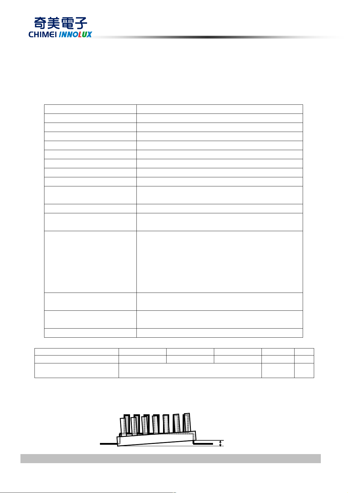
I/F connector mounting position
Note (1) Please refer to the attached drawings for more information of front and back outline dimensions.
The mounting inclination of the connector makes the
screen center within ± 0.5mm as the horizontal.
(2)
Note (2) Connector mounting position
Version 2.0 5 Date::::08 Apr. 2011
The copyright belongs to CHIMEI InnoLux. Any unauthorized use is prohibited
+/- 0.5mm
Page 6
PRODUCT SPECIFICATION
2. ABSOLUTE MAXIMUM RATINGS
2.1 ABSOLUTE RATINGS OF ENVIRONMENT
Value
Item Symbol
Min. Max.
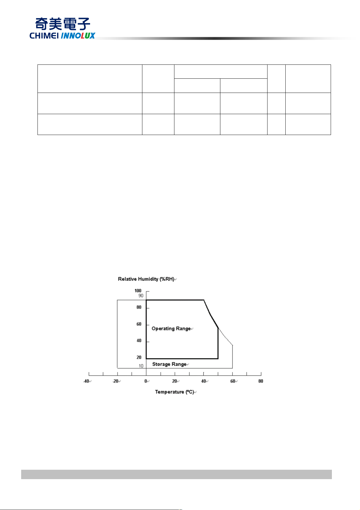
Storage Temperature TST -20 +60 ºC
Operating Ambient Temperature TOP 0 50 ºC
Note (1)Temperature and relative humidity range is shown in the figure below.
(a) 90 %RH Max. (Ta ≦ 40 ºC).
(b) Wet-bulb temperature should be 39 ºC Max. (Ta > 40 ºC).
(c) No condensation.
Note (2) The maximum operating temperature is based on the test condition that the surface temperature of
Unit
Note
(1)
With CMI
Module
(1), (2)
With CMI
Module
display area is less than or equal to 65 ºC with LCD module alone in a temperature controlled chamber.
Thermal management should be considered in final product design to prevent the surface temperature of
display area from being over 65 ºC. The range of operating temperature may degrade in case of
improper thermal management in final product design.
Version 2.0 6 Date::::08 Apr. 2011
The copyright belongs to CHIMEI InnoLux. Any unauthorized use is prohibited
Page 7
PRODUCT SPECIFICATION
2.2 ABSOLUTE RATINGS OF ENVIRONMENT (OPEN CELL)
Recommended Storage Condition: With shipping package.
Recommended Storage temperature range: 25±5 ℃
Recommended Storage humidity range: 50±10%RH
Recommended Shelf life: a month
2.3 ELECTRICAL ABSOLUTE RATINGS
2.3.1 TFT LCD OPEN CELL
Value
Item Symbol
Min. Max.
Voltage for gate driver VGH -0.3 40 V
Unit Note
Voltage for gate driver VGL -20 0.3 V
Voltage range for gate driver VGH - VGL -0.3 43 V
Voltage for data diver VAA 12 18 V
Logic Input Voltage VIN -0.3 5 V
Version 2.0 7 Date::::08 Apr. 2011
The copyright belongs to CHIMEI InnoLux. Any unauthorized use is prohibited
Page 8

3. ELECTRICAL CHARACTERISTICS
Voltage for gate driver
Voltage for gate driver
Voltage range for gate driver
Voltage for data driver
Voltage for data driver
3.1 TFT LCD OPEN CELL
(Ta = 25 ± 2 ºC)
Parameter Symbol
VGH 29 30 31 V
VGL -7.7 -8 -8.3 V
VGH - VGL 36.7 38 39.3 V
VAA 17.4 17.7 18 V
VAAM 8.4 8.7 9.0 V
PRODUCT SPECIFICATION
Value
Unit Note
Min. Typ. Max.
Differential Input High
Threshold Voltage
Differential Input Low
Threshold Voltage
Mini- LVDS
interface
CMOS
interface
Note (1) The Mini- LVDS input characteristics are as follows:
Common Input Voltage VCM 1.0 1.2 1.4 V
Differential input voltage |VID| 200
Terminating Resistor RT
Input High Threshold Voltage
Input Low Threshold Voltage VIL 0
V
LVTH
V
LVTL
VIH 2.7
+100
- -
-
- -
-100 mV
-
100
-
-
600 mV
3.3 V
0.7 V
-
mV
(1)
ohm
Version 2.0 8 Date::::08 Apr. 2011
The copyright belongs to CHIMEI InnoLux. Any unauthorized use is prohibited
Page 9
3.2 CIRCUIT AND WIRING DIAGRAM OF SPWB
PRODUCT SPECIFICATION
Mini-LVDS signal: 6path-6pair.
Control signals of data drivers.
(CLK )
Voltages of data drivers.
Control signals and voltages of scan drivers.
Version 2.0 9 Date::::08 Apr. 2011
The copyright belongs to CHIMEI InnoLux. Any unauthorized use is prohibited
Page 10
3.3 SPWB INFORMATION
PRODUCT SPECIFICATION
Version 2.0 10 Date::::08 Apr. 2011
The copyright belongs to CHIMEI InnoLux. Any unauthorized use is prohibited
Page 11
PRODUCT SPECIFICATION
4. INPUT TERMINAL PIN ASSIGNMENT
4.1 TFT LCD OPEN CELL
CN1 ( XLL ) Connector Pin Assignment ::::P-TWO 196318-80041-3
Pin Name Description Note
1 GND Ground
2 MLA0P Mini-LVDS data signal+
3 MLA0N Mini-LVDS data signal4 MLA1P Mini-LVDS data signal+
5 MLA1N Mini-LVDS data signal6 MLA2P Mini-LVDS data signal+
7 MLA2N Mini-LVDS data signal-
8 GND Ground
9 MLCCKP Mini-LVDS clock signal+
10 MLCCKN Mini-LVDS clock signal11 GND Ground
12 MLA4P Mini-LVDS data signal+
13 MLA4N Mini-LVDS data signal14 MLA5P Mini-LVDS data signal+
15 MLA5N Mini-LVDS data signal16 MLA6P Mini-LVDS data signal+
17 MLA6N Mini-LVDS data signal18 GND Ground
19 GND Ground
20 VGH Scan driver voltage
21 VGH Scan driver voltage
22 GND Ground
23 VGL Scan driver voltage
24 VGL Scand driver voltage
25 GND Ground
26 OE1 Scan driver output enable
27 OE2 Scan driver output enable
28 CKV Scan driver clock
29 STV2 Scan driver start pulse
30 PAIRMODE Selects mini-LVDS input mode
31 POL Data driver polarity invert
32 VDASEL Half VAA selection
33 TP1 Data driver data latch
34 CSTV Scan driver start pulse
35 GND Ground
36 GM18 Gamma voltage
37 GM17
38 GM16 Gamma voltage
39 GM13 Gamma voltage
40 GM12 Gamma voltage
41 GM10 Gamma voltage
42 GM9 Gamma voltage
43 GM7 Gamma voltage
44 GM6 Gamma voltage
45 GM3 Gamma voltage
46 GM2 Gamma voltage
47 GM1 Gamma voltage
48 GND Ground
49 VDD Logic power
50 VDD Logic power
Gamma voltage
(1)
Version 2.0 11 Date::::08 Apr. 2011
The copyright belongs to CHIMEI InnoLux. Any unauthorized use is prohibited
Page 12
PRODUCT SPECIFICATION
51 GND Ground
52 VDDAM Half VAA voltage
53 VDDAM Half VAA voltage
54 GND Ground
55 VCM VCOM voltage
56 VCM VCOM voltage
57 GND Ground
58 VDDA VAA voltage
59 VDDA VAA voltage
60 GND Ground
CN1 ( XLR ) Connector Pin Assignment ::::P-TWO 196318-80041-3
Pin Name Description Note
1 GND Ground
2 VDDA VAA voltage
3 VDDA VAA voltage
4 GND Ground
5 VCM VCOM voltage
6 VCM VCOM voltage
7 GND Ground
8 VDDAM Half VAA voltage
9 VDDAM Half VAA voltage
10 GND Ground
11 VDD Logic power
12 VDD Logic power
13 GND Ground
14 GM1 Gamma voltage
15 GM2 Gamma voltage
16 GM3 Gamma voltage
17 GM6 Gamma voltage
18 GM7 Gamma voltage
19 GM9 Gamma voltage
20 GM10 Gamma voltage
21 GM12 Gamma voltage
22 GM13 Gamma voltage
23 GM16 Gamma voltage
24 GM17 Gamma voltage
25 GM18 Gamma voltage
26 GND Ground
27 CSTV Scan driver start pulse
28 TP1 Data driver data latch
29 VDASEL Half VAA selection
30 POL Data driver polarity invert
31 PAIRMODE Selects mini-LVDS input mode
32 STV2 Scan driver start pulse
33 CKV Scan driver clock
34 OE2 Scan driver output enable
35 OE1 Scan driver output enable
36 GND Ground
37 VGL Scan driver voltage
38 VGL Scand driver voltage
39 GND Ground
40 VGH Scan driver voltage
41 VGH Scan driver voltage
42 GND Ground
(1)
Version 2.0 12 Date::::08 Apr. 2011
The copyright belongs to CHIMEI InnoLux. Any unauthorized use is prohibited
Page 13

PRODUCT SPECIFICATION
43 GND Ground
44 MLA6N Mini-LVDS data signal45 MLA6P Mini-LVDS data signal+
46 MLA5N Mini-LVDS data signal47 MLA5P Mini-LVDS data signal+
48 MLA4N Mini-LVDS data signal49 MLA4P Mini-LVDS data signal+
50 GND Ground
MLACKN
51
52 MLACKP Mini-LVDS clock signal+
53 GND Ground
54 MLA2N Mini-LVDS data signal55 MLA2P Mini-LVDS data signal+
56 MLA1N Mini-LVDS data signal57 MLA1P Mini-LVDS data signal+
58 MLA0N Mini-LVDS data signal59 MLA0P Mini-LVDS data signal+
60 GND Ground
CN2 ( XLR ) Connector Pin Assignment ::::P-TWO 196225-80041
Pin Name Description Note
1 MLC6N Mini-LVDS data signal-
2 MLC6P Mini-LVDS data signal+
3 MLC5N Mini-LVDS data signal-
4 MLC5P Mini-LVDS data signal+
5 MLC4N Mini-LVDS data signal-
6 MLC4P Mini-LVDS data signal+
7 GND Ground
8 MLCCKN Mini-LVDS clock signal-
9 MLCCKP Mini-LVDS clock signal+
10 GND Ground
11 MLC2N Mini-LVDS data signal12 MLC2P Mini-LVDS data signal+
13 MLC1N Mini-LVDS data signal14 MLC1P Mini-LVDS data signal+
15 MLC0N Mini-LVDS data signal16 MLC0P Mini-LVDS data signal+
17 GND Ground
18 MLB6N Mini-LVDS data signal19 MLB6P Mini-LVDS data signal+
20 MLB5N Mini-LVDS data signal21 MLB5P Mini-LVDS data signal+
22 MLB4N Mini-LVDS data signal23 MLB4P Mini-LVDS data signal+
24 GND Ground
25 MLBCKN Mini-LVDS clock signal26 MLBCKP Mini-LVDS clock signal+
27 GND Ground
28 MLB2N Mini-LVDS data signal29 MLB2P Mini-LVDS data signal+
30 MLB1N Mini-LVDS data signal31 MLB1P Mini-LVDS data signal+
32 MLB0N Mini-LVDS data signal33 MLB0P Mini-LVDS data signal+
34 GND Ground
Mini-LVDS clock signal-
Version 2.0 13 Date::::08 Apr. 2011
The copyright belongs to CHIMEI InnoLux. Any unauthorized use is prohibited
Page 14

35 STV2 Scan driver start pulse
36 CSTV Scan driver start pulse
37 POL Data driver polarity invert
38 CKV Scan driver clock
39 TP1 Data driver data latch
40 OE2 Scan driver output enable
41 OE1 Scan driver output enable
42 GND Ground
43 GM18 Gamma voltage
44 GM17
45 GM16 Gamma voltage
46 NC No connection
47 NC No connection
48 GM13 Gamma voltage
49 GM12 Gamma voltage
50 NC No connection
51 GM10 Gamma voltage
52 GM9 Gamma voltage
53 NC No connection
54 GM7 Gamma voltage
55 GM6 Gamma voltage
56 NC No connection
57 NC No connection
58 GM3 Gamma voltage
59 GM2 Gamma voltage
60 GM1 Gamma voltage
61 GND Ground
62 VDDA VAA voltage
63 VDDA VAA voltage
64 VDDA VAA voltage
65 GND Ground
66 VDDAM Half VAA voltage
67 VDDAM Half VAA voltage
68 GND Ground
69 VCM VCOM voltage
70 VCM VCOM voltage
71 GND Ground
72 VDD Logic power
73 VDD Logic power
74 GND Ground
75 VGL Scan driver voltage
76 VGL Scan driver voltage
77 GND Ground
78 VGH Scan driver voltage
79 VGH Scand driver voltage
80 VGH Scand driver voltage
Gamma voltage
PRODUCT SPECIFICATION
CN3 ( XLR ) Connector Pin Assignment ::::Starconn B-F,089H55-000000-G2-R
Pin Name Description Note
1 GND Ground
2 MLA6N Mini-LVDS data signal-
3 MLA6P Mini-LVDS data signal+
4 MLA5N Mini-LVDS data signal-
5 MLA5P Mini-LVDS data signal+
6 MLA4N Mini-LVDS data signal-
Version 2.0 14 Date::::08 Apr. 2011
The copyright belongs to CHIMEI InnoLux. Any unauthorized use is prohibited
Page 15

7 MLA4P Mini-LVDS data signal+
8 GND Ground
9 MLACKN Mini-LVDS clock signal10 MLACKP Mini-LVDS clock signal+
11 GND Ground
12 MLA2N Mini-LVDS data signal13 MLA2P Mini-LVDS data signal+
14 MLA1N Mini-LVDS data signal15 MLA1P Mini-LVDS data signal+
16 MLA0N Mini-LVDS data signal17 MLA0P Mini-LVDS data signal+
18 GND Ground
19 NC No connection
20 NC No connection
21 NC No connection
22 NC No connection
23 GND Ground
24 NC No connection
25 NC No connection
26 GND Ground
27 GND Ground
28 GND Ground
29 GND Ground
30 GND Ground
31 GND Ground
32 NC No connection
33 NC No connection
34 NC No connection
35 NC No connection
36 NC No connection
37 NC No connection
38 NC No connection
39 NC No connection
40 GND Ground
41 NC No connection
42 NC No connection
43 GND Ground
44 NC No connection
45 NC No connection
46 NC No connection
47 NC No connection
48 NC No connection
49 NC No connection
50 NC No connection
51 NC No connection
52 NC No connection
53 NC No connection
54 NC No connection
55 GND Ground
PRODUCT SPECIFICATION
CN1 ( XRR ) Connector Pin Assignment ::::P-TWO 196318-80041-3
Pin Name Description Note
1 GND Ground
2 VDDA VAA voltage
3 VDDA VAA voltage
Version 2.0 15 Date::::08 Apr. 2011
The copyright belongs to CHIMEI InnoLux. Any unauthorized use is prohibited
Page 16

PRODUCT SPECIFICATION
4 GND Ground
5 VCM VCOM voltage
6 VCM VCOM voltage
7 GND Ground
8 VDDAM Half VAA voltage
9 VDDAM Half VAA voltage
10 GND Ground
11 VDD Logic power
12 VDD Logic power
13 GND Ground
14 GM1 Gamma voltage
15 GM2 Gamma voltage
16 GM3 Gamma voltage
17 GM6 Gamma voltage
18 GM7 Gamma voltage
19 GM9 Gamma voltage
20 GM10 Gamma voltage
21 GM12 Gamma voltage
22 GM13 Gamma voltage
23 GM16 Gamma voltage
24 GM17 Gamma voltage
25 GM18 Gamma voltage
26 GND Ground
27 CSTV Scan driver start pulse
28 TP1 Data driver data latch
29 VDASEL Half VAA selection
30 POL Data driver polarity invert
31 PAIRMODE Selects mini-LVDS input mode
32 STV2 Scan driver start pulse
33 CKV Scan driver clock
34 OE2 Scan driver output enable
35 OE1 Scan driver output enable
36 GND Ground
37 VGL Scan driver voltage
38 VGL Scand driver voltage
39 GND Ground
40 VGH Scan driver voltage
41 VGH Scan driver voltage
42 GND Ground
43 GND Ground
44 MLF0P Mini-LVDS data signal+
45 MLF0N Mini-LVDS data signal46 MLF1P Mini-LVDS data signal+
47 MLF1N Mini-LVDS data signal48 MLF2P Mini-LVDS data signal+
49 MLF2N Mini-LVDS data signal50 GND Ground
MLFCKP
51
52 MLFCKN Mini-LVDS clock signal53 GND Ground
54 MLF4P Mini-LVDS data signal+
55 MLF4N Mini-LVDS data signal56 MLF5P Mini-LVDS data signal+
57 MLF5N Mini-LVDS data signal58 MLF6P Mini-LVDS data signal+
59 MLF6N Mini-LVDS data signal-
Mini-LVDS clock signal+
Version 2.0 16 Date::::08 Apr. 2011
The copyright belongs to CHIMEI InnoLux. Any unauthorized use is prohibited
(1)
Page 17

PRODUCT SPECIFICATION
60 GND Ground
CN1 ( XRL ) Connector Pin Assignment ::::P-TWO 196318-80041-3
Pin Name Description Note
1 GND Ground
2 MLF6N Mini-LVDS data signal-
3 MLF6P Mini-LVDS data signal+
4 MLF5N Mini-LVDS data signal-
5 MLF5P Mini-LVDS data signal+
6 MLF4N Mini-LVDS data signal-
7 MLF4P Mini-LVDS data signal+
8 GND Ground
9 MLFCKN Mini-LVDS clock signal-
MLFCKP
10
11 GND Ground
12 MLF3N Mini-LVDS data signal13 MLF3P Mini-LVDS data signal+
14 MLF2N Mini-LVDS data signal15 MLF2P Mini-LVDS data signal+
16 MLF1N Mini-LVDS data signal17 MLF1P Mini-LVDS data signal+
18 GND Ground
19 GND Ground
20 VGH Scan driver voltage
21 VGH Scan driver voltage
22 GND Ground
23 VGL Scan driver voltage
24 VGL Scand driver voltage
25 GND Ground
26 OE1 Scan driver output enable
27 OE2 Scan driver output enable
28 CKV Scan driver clock
29 STV2 Scan driver start pulse
30 PAIRMODE Selects mini-LVDS input mode
31 POL Data driver polarity invert
32 VDASEL Half VAA selection
33 TP1 Data driver data latch
34 CSTV Scan driver start pulse
35 GND Ground
36 GM18 Gamma voltage
37 GM17 Gamma voltage
38 GM16 Gamma voltage
39 GM13 Gamma voltage
40 GM12 Gamma voltage
41 GM10 Gamma voltage
42 GM9 Gamma voltage
43 GM7 Gamma voltage
44 GM6 Gamma voltage
45 GM3 Gamma voltage
46 GM2 Gamma voltage
47 GM1 Gamma voltage
48 GND Ground
49 VDD Logic power
50 VDD Logic power
51 GND Ground
Mini-LVDS clock signal+
(1)
Version 2.0 17 Date::::08 Apr. 2011
The copyright belongs to CHIMEI InnoLux. Any unauthorized use is prohibited
Page 18

PRODUCT SPECIFICATION
52 VDDAM Half VAA voltage
53 VDDAM Half VAA voltage
54 GND Ground
55 VCM VCOM voltage
56 VCM VCOM voltage
57 GND Ground
58 VDDA VAA voltage
59 VDDA VAA voltage
60 GND Ground
CN2 ( XRL ) Connector Pin Assignment ::::P-TWO 196225-80041
Pin Name Description Note
1 VGH Scan driver voltage
2 VGH Scand driver voltage
3 VGH Scand driver voltage
4 GND Ground
5 VGL Scan driver voltage
6 VGL Scan driver voltage
7 GND Ground
8 VDD Logic power
9 VDD Logic power
10 GND Ground
11 VCM VCOM voltage
12 VCM VCOM voltage
13 GND Ground
14 VDDAM Half VAA voltage
15 VDDAM Half VAA voltage
16 GND Ground
17 VDDA VAA voltage
18 VDDA VAA voltage
19 VDDA VAA voltage
20 GND Ground
21 GM1 Gamma voltage
22 GM2 Gamma voltage
23 GM3 Gamma voltage
24 GND Ground
25 GND Ground
26 GM6 Gamma voltage
27 GM7 Gamma voltage
28 GND Ground
29 GM9 Gamma voltage
30 GM10 Gamma voltage
31 GND Ground
32 GM12 Gamma voltage
33 GM13 Gamma voltage
34 GND Ground
35 GND Ground
36 GM16 Gamma voltage
37 GM17 Gamma voltage
38 GM18 Gamma voltage
39 GND Ground
40 STV2 Scan driver start pulse
41 CSTV Scan driver start pulse
42 POL Data driver polarity invert
43 CKV Scan driver clock
Version 2.0 18 Date::::08 Apr. 2011
The copyright belongs to CHIMEI InnoLux. Any unauthorized use is prohibited
Page 19

44 TP1 Data driver data latch
45 OE2 Scan driver output enable
46 OE1 Scan driver output enable
47 GND Ground
48 MLE6N Mini-LVDS data signal49 MLE6P Mini-LVDS data signal+
50 MLE5N Mini-LVDS data signal51 MLE5P Mini-LVDS data signal+
52 MLE4N Mini-LVDS data signal53 MLE4P Mini-LVDS data signal+
54 GND Ground
55 MLECKN Mini-LVDS clock signal56 MLECKP Mini-LVDS clock signal+
57 GND Ground
58 MLE2N Mini-LVDS data signal59 MLE2P Mini-LVDS data signal+
60 MLE1N Mini-LVDS data signal61 MLE1P Mini-LVDS data signal+
62 MLE0N Mini-LVDS data signal63 MLE0P Mini-LVDS data signal+
64 GND Ground
65 MLD6N Mini-LVDS data signal66 MLD6P Mini-LVDS data signal+
67 MLD5N Mini-LVDS data signal68 MLD5P Mini-LVDS data signal+
69 MLD4N Mini-LVDS data signal70 MLD4P Mini-LVDS data signal+
71 GND Ground
72 MLDCKN Mini-LVDS clock signal73
74 GND Ground
75 MLD2N Mini-LVDS data signal76 MLD2P Mini-LVDS data signal+
77 MLD1N Mini-LVDS data signal78 MLD1P Mini-LVDS data signal+
79 MLD0N Mini-LVDS data signal80 MLD0P Mini-LVDS data signal+
MLDCKP
Mini-LVDS clock signal+
PRODUCT SPECIFICATION
CN3 ( XRL ) Connector Pin Assignment ::::Starconn B-F,089H55-000000-G2-R
Pin Name Description Note
1 GND Ground
2 NC No connection
3 NC No connection
4 NC No connection
5 NC No connection
6 NC No connection
7 NC No connection
8 NC No connection
9 NC No connection
10 NC No connection
11 NC No connection
12 NC No connection
13 GND Ground
14 NC No connection
15 NC No connection
Version 2.0 19 Date::::08 Apr. 2011
The copyright belongs to CHIMEI InnoLux. Any unauthorized use is prohibited
Page 20

PRODUCT SPECIFICATION
16 GND Ground
17 NC No connection
18 NC No connection
19 NC No connection
20 NC No connection
21 NC No connection
22 NC No connection
23 NC No connection
24 NC No connection
25 GND Ground
26 GND Ground
27 GND Ground
28 GND Ground
29 GND Ground
30 GND Ground
31 NC No connection
32 NC No connection
33 GND Ground
34 NC No connection
35 NC No connection
36 NC No connection
37 NC No connection
38 GND Ground
39 MLF6N Mini-LVDS data signal40 MLF6P Mini-LVDS data signal+
41 MLF5N Mini-LVDS data signal42 MLF5P Mini-LVDS data signal+
43 MLF4N Mini-LVDS data signal44 MLF4P Mini-LVDS data signal+
45 GND Ground
46 MLFCKN Mini-LVDS clock signal47 MLFCKP Mini-LVDS clock signal+
48 GND Ground
49 MLF2N Mini-LVDS data signal50 MLF2P Mini-LVDS data signal+
51 MLF1N Mini-LVDS data signal52 MLF1P Mini-LVDS data signal+
53 MLF0N Mini-LVDS data signal54 MLF0P Mini-LVDS data signal+
55 GND Ground
Note (1) VDA select: Half/Full VAA operating range selection.
Low = Connect to GND, High = Connect to +3.3V
VDA SEL Note
L Full VAA
H Half VAA (V460H1-PE5 setting)
Version 2.0 20 Date::::08 Apr. 2011
The copyright belongs to CHIMEI InnoLux. Any unauthorized use is prohibited
Page 21

PRODUCT SPECIFICATION
Note (2)The screw hole which is distant from the connector is merged with Ground
4.2 FLICKER (Vcom) ADJUSTMENT
(1) Adjustment Pattern:
Sub-pixel on-off pattern was shown as below. If customer need below pattern, please directly contact with
Account FAE.
(bright sub-pixel:G128 ; dark sub-pixel:G0)
(2) Adjustment method: (Digital V-com)
Programmable memory IC is used for Digital V-com adjustment in this model. CMI provide Auto Vcom tools
to adjust Digital V-com.The detail connection and setting instruction, please directly contact with Account
FAE or refer CMI Auto V-com adjustment OI. Below items is suggested to be ready before Digital V-com
adjustment in customer LCM line.
a. USB Sensor Board.
b. Programmable software.
Version 2.0 21 Date::::08 Apr. 2011
The copyright belongs to CHIMEI InnoLux. Any unauthorized use is prohibited
Page 22

PRODUCT SPECIFICATION
5. INTERFACE TIMING
5.1 INPUT SIGNAL TIMING SPECIFICATIONS
(Ta = 25 ± 2 ºC)
The input signal timing specifications are shown as the following table and timing diagram.
Test condition :LVDS Receiver Clock 74.25MHz
Signal Item Symbol Typ
TP1 start TP1_STR 0.33 us
TP1
TP1 pulse width TP1_PW 6.9 us
OE1 start OE1_STR 5.7 us
OE1 pulse width OE1_PW 1.63 us
OE
OE2 start OE2_STR 3.24 us
OE2_PW OE2_PW 4.09 us
STV
CKV Scan driver clock CKV 3.77 us
POL
Data arrangement 2D2G
Scan driver start
pulse
Data driver polarity
invert
STV 3.77 us
POL 4.16 us
Unit
Version 2.0 22 Date::::08 Apr. 2011
The copyright belongs to CHIMEI InnoLux. Any unauthorized use is prohibited
Page 23

PRODUCT SPECIFICATION
LCLK+
LCLK+
LCLK+
LCLK+
LV0+/-
LV0+/-
LV0+/-
LV0+/-
LV0+/- to
LV0+/- to
LV0+/- to
LV0+/- to
LV2+/-
LV2+/-
LV2+/-
LV2+/-
TP1
TP1
TP1
TP1
LCLK+
LCLK+
LV0+/-
LV0+/-
LV0+/- to
LV0+/- to
LV2+/-
LV2+/-
Data Data
Data Data
Data Data
Data Data
Data Data
Data Data
Data Data
Data Data
Data Data
Data Data
Data Data
Data Data
RST=L RST=L
RST=L RST=L
NA NA
NA NA
Data
Data
Data
Data
Data
Data
Data
Data
Data
Data
Data
Data
NA NA
NA NA
NA NA
NA NA
Data
Data
Data
Data
Data
Data
Data
Data
Data
Data
Data
Data
NA NA
NA NA
NA NA
NA NA
TP1_STR TP1_PW
TP1_STR TP1_PW
TP1_STR TP1_PW
TP1_STR TP1_PW
NA
RST=H
RST=H
NA
NA
RST=H
RST=H
NA
NA
RST=H NA
RST=H NA
NA NA
NA NA
RST=L
RST=L
NA NA
NA NA
NA
NA NA
NA NA
NA NA
NA NA
NA NA
NA NA
NA NA
NA NA
Data
Data
Data
Data
Data
Data
RST=L
RST=L
RST=L
RST=L
RST=L
RST=L
RST=L
RST=L
Data
Data
Data
Data
Data
Data
RST=L
RST=L
RST=L
RST=L
RST=L
RST=L
RST=L
RST=L
Data Data
Data Data
Data Data
Data Data
Data Data
Data Data
Data Data
Data Data
Data Data
Data Data
Data Data
Data Data
Data Data
Data Data
Data
Data
Data
Data
Data
Data
Data
Data
Data
Data
Data
Data
Data Data
Data Data
Data Data
Data Data
Data Data
Data Data
(STH)
(STH)
OE1
OE1
OE1_STR OE1_PW
OE1_STR OE1_PW
OE2
OE2
OE2_STR OE2_PW
OE2_STR OE2_PW
Version 2.0 23 Date::::08 Apr. 2011
The copyright belongs to CHIMEI InnoLux. Any unauthorized use is prohibited
Page 24

LCLK+
LCLK+
LV0+/-
LV0+/-
LV1+/- to
LV1+/- to
LV5+/-
LV5+/-
(STH)
(STH)
RST=H
RST=H
NA
NA
RST=H
RST=H
NA
NA
RST=H NA
RST=H NA
NA NA
NA NA
PRODUCT SPECIFICATION
RST=H
RST=H
RST=H
NA
NA
NA
RST=H
RST=H
RST=H
NA
NA
NA
RST=H
RST=H
RST=H
NA NA
NA NA
NA NA
NA
NA
NA
RST=H
RST=H
RST=H
NA
NA
NA
RST=H
RST=H
RST=H
NA
NA
NA
RST=H
RST=H
RST=H
NA NA
NA NA
NA NA
NA
NA
NA
½ mini-LVDS data
½ mini-LVDS data
½ mini-LVDS data
½ mini-LVDS data
STV
STV
CKV
CKV
mini-LVDS data end mini-LVDS data end
mini-LVDS data end mini-LVDS data end
TP1
TP1
POL hold time
POL hold time
POL setup time
POL setup time
POL
POL
Version 2.0 24 Date::::08 Apr. 2011
The copyright belongs to CHIMEI InnoLux. Any unauthorized use is prohibited
Page 25

Note: Data arrangement of 2G2D
R
R
R
1
1
1
1
1
1
G
G
G
1
1
1
1
1
1
B
B
B
1
1
1
1
1
1
PRODUCT SPECIFICATION
Data driver
Data driver
R
R
R
2
2
2
1
1
1
G
G
G
2
2
2
1
1
1
B
B
B
2
2
2
1
1
1
R
R
R
1920
1920
1920
1
1
1
G
G
G
1920
1920
1920
1
1
1
B
B
B
1920
1920
1920
1
1
1
R
R
R
1
1
1
2
2
2
R
R
R
1
1
1
3
3
3
R
R
R
1
1
1
4
4
4
G
G
G
1
1
1
2
2
2
G
G
G
1
1
1
3
3
3
G
G
G
1
1
1
4
4
4
B
B
B
1
1
1
2
2
2
B
B
B
1
1
1
3
3
3
B
B
B
1
1
1
4
4
4
R
R
R
2
2
2
2
2
2
R
R
R
2
2
2
3
3
3
R
R
R
2
2
2
4
4
4
G
G
G
2
2
2
2
2
2
G
G
G
2
2
2
3
3
3
G
G
G
2
2
2
4
4
4
B
B
B
2
2
2
2
2
2
B
B
B
2
2
2
3
3
3
B
B
B
2
2
2
4
4
4
R
R
R
1920
1920
1920
2
2
2
R
R
R
1920
1920
1920
3
3
3
R
R
R
1920
1920
1920
4
4
4
G
G
G
1920
1920
1920
2
2
2
G
G
G
1920
1920
1920
3
3
3
G
G
G
1920
1920
1920
4
4
4
B
B
B
1920
1920
1920
2
2
2
B
B
B
1920
1920
1920
3
3
3
B
B
B
1920
1920
1920
4
4
4
Version 2.0 25 Date::::08 Apr. 2011
The copyright belongs to CHIMEI InnoLux. Any unauthorized use is prohibited
Page 26

6. OPTICAL CHARACTERISTICS
6.1 TEST CONDITIONS
Item Symbol Value Unit
Ambient Temperature Ta
PRODUCT SPECIFICATION
o
25±2
C
Ambient Humidity Ha
Vertical Frame Rate
Fr 240 Hz
50±10
%RH
6.2 OPTICAL SPECIFICATIONS
The relative measurement methods of optical characteristics are shown as below. The following items
should be measured under the test conditions described in 6.1 and stable environment shown in 6.1.
Item Symbol
Rcx
Condition Min. Typ. Max. Unit Note
0.656
-
Red
Color
Chromaticity
Green
Blue
Rcy
Gcx
Gcy
Bcx
Bcy
Wcx
θ
=0°, θY =0°
x
Viewing Angle at Normal
Direction
Standard light source “C”
Typ.-
0.03
0.326
0.261
0.581
0.131
0.114
0.290
Typ.+
0.03
-
-
-
-
-
-
White
Wcy
0.345
-
(0)(6)
Center Transmittance T% - 4.6 - % (1),(5)
Contrast Ratio CR
TR -
Response Time
TF
θ
=0°, θY =0°
x
with CMI module
θx=0°, θY =0°
with CMI
Module@120Hz,
Panel temperature is
4000 5000
25 -
-
4.0 -
- - (1),(3)
ms
(1),(4)
ms
34±1℃
88
88
88
88
-
Deg. (1),(2)
-
-
Viewing
Angle
Horizontal
Vertical
θ
+
x
θ
-
x
θ
+
Y
θ
-
Y
CR≥20
With CMI module
80
80
80
80
Note (0) Light source is the standard light source “C” which is defined by CIE and driving voltages are based on
suitable gamma voltages. The calculating method is as following:
1. Measure Module’s and BLU’s spectrums. W, R, G, B are with signal input. BLU ( for V645H1-LE1 ) is
supplied by CMI.
2. Calculate cell’s spectrum.
3. Calculate cell’s chromaticity by using the spectrum of standard light source “C”
Version 2.0 26 Date::::08 Apr. 2011
The copyright belongs to CHIMEI InnoLux. Any unauthorized use is prohibited
Page 27

PRODUCT SPECIFICATION
Time
Note (1) Light source is the BLU which supplied by CMI and driving voltage are based on suitable gamma voltages.
Note (2) Definition of Viewing Angle (θx, θy):
Viewing angles are measured by Autronic Conoscope Cono-80
θ
X-
= 90º
x-
6 o’clock
θ
y-
= 90º
y-
Note (3) Definition of Contrast Ratio (CR):
The contrast ratio can be calculated by the following expression.
Normal
θx = θy = 0º
θy+
θx−
θx+
12 o’clock direction
y+
θ
y+
= 90º
x+
θ
X+
= 90º
Contrast Ratio (CR) =
L255: Luminance of gray level 255
L 0: Luminance of gray level 0
CR = CR (5), where CR (X) is corresponding to the Contrast Ratio of the point X at the figure in Note (6).
Note (4) Definition of Response Time (TR, TF,) :
100%
90%
Optical
Response
10%
0%
Gray to gray
switching time
L255 of Luminance Surface
L0 of Luminance Surface
Gray to gray
switching time
Version 2.0 27 Date::::08 Apr. 2011
The copyright belongs to CHIMEI InnoLux. Any unauthorized use is prohibited
Page 28

TR means switching time from gray 0 to 255
500 mm
LCD
LCD
Light Shield Room
l
TF means switching time from gray 255 to 0
Note (5) Definition of Transmittance (T%) :
Measure the luminance of gray level 255 at center point of LCD module.
PRODUCT SPECIFICATION
Transmittance (T%) =
Film structure : 3 pieces of Diffusers
Note (6) Measurement Setup:
The LCD module should be stabilized at given temperature for 1 hour to avoid abrupt temperature
change during measuring. In order to stabilize the luminance, the measurement should be
executed after lighting backlight for 1 hour in a windless room.
Module
Panel
module LCD of Luminance
unit backligh of Luminance
×
CS -2000
100%
Field of View = 1º
(Ambient
Luminance < 2
ux)
Version 2.0 28 Date::::08 Apr. 2011
The copyright belongs to CHIMEI InnoLux. Any unauthorized use is prohibited
Page 29

7. RELIABILITY TEST CONDITION
Contact Mode
NO.
Test Item Test Condition
PRODUCT SPECIFICATION
1 HT Operation
2 HT Storage
3 LT Operation
4 LT Storage
5 HTHH Operation
6 HTHH Storage
Thermal Shock
7
(Non-operation)
8 Image Sticking
ESD-Air mode
9
Discharge
Ta=50℃, 1000hrs
Ta=60℃, 500hrs
Ta=0℃, 500hrs
Ta=-20℃, 500hrs
Ta=50℃/ 80%RH, 500hrs
Ta=50℃/ 90%RH, 500hrs
[(-20℃ 30min)→(60℃ 30min)]/cycle, 200cycles
Ta=50℃, 300hrs
150pf,330Ω, ±15KV (operation) Class C ( With CMI Module )
ESD-
10
Discharge
11 Packing Vibration
12 Packing Drop Bottom 20cm+ 4 edges with 15 angle
150pf,330Ω, ±8KV (operation) Class B ( With CMI Module)
1.14Grms Random frequency 1~200Hz 30min/Bottom, 15min/Right-Left,
15min/Front-Back
Version 2.0 29 Date::::08 Apr. 2011
The copyright belongs to CHIMEI InnoLux. Any unauthorized use is prohibited
Page 30

PRODUCT SPECIFICATION
8. PRECAUTIONS
8.1 ASSEMBLY AND HANDLING PRECAUTIONS
[ 1 ] Do not apply rough force such as bending or twisting to the module during assembly.
[ 2 ] It is recommended to assemble or to install a module into the user’s system in clean working areas. The
dust and oil may cause electrical short or worsen the polarizer.
[ 3 ] Do not apply pressure or impulse to the module to prevent the damage of LCD panel.
[ 4 ] Always follow the correct power-on sequence when the LCD module is turned on. This can prevent the
damage and latch-up of the CMOS LSI chips.
[ 5 ] The distance between COF edge and rib of BLU is suggested to be larger than 5mm, in order to prevent
from damage on COF during module assembly.
[ 6 ] Do not design sharp-pointed structure / parting line / tooling gate on the COF position of plastic parts,
because the burr will scrape the COF.
[ 7 ] If COF would be bended during module assembly, it is suggested not to locate the IC on the bending corner
of COF.
[ 8 ] The gap between COF IC and any structure of BLU is suggested to be larger than 2mm, in order to prevent
from damage on COF IC.
[ 9 ] Bezel opening must have no burr. Burr will scrape the panel surface.
[ 10 ] It is suggested that bezel of module and bezel of TV set can not press or touch the panel surface. It will
make light leakage or scrape.
[ 11 ] When module used FFC / FPC, but no FFC / FPC to be attached in the open cell. Customer can refer the
FFC / FPC drawing and buy it by self.
[ 12 ] The gap between Panel and any structure of Bezel is suggested to be larger than 2mm, in order to prevent
from damage on Panel.
[ 13 ] Do not plug in or pull out the I/F connector while the module is in operation.
[ 14 ] Use a soft dry cloth without chemicals for cleaning, because the surface of polarizer is very soft and easily
scratched.
[ 15 ] Moisture can easily penetrate into LCD module and may cause the damage during operation.
[ 16 ] When storing modules as spares for a long time, the following precaution is necessary.
[ 16.1 ] Do not leave the module in high temperature, and high humidity for a long time. It is highly
recommended to store the module with temperature from 0 to 35℃at normal humidity without
condensation.
[ 16.2 ] The module shall be stored in dark place. Do not store the TFT-LCD module in direct sunlight or
fluorescent light.
[ 17 ] When ambient temperature is lower than 10ºC, the display quality might be reduced.
[ 18 ] The peeling strength of COF is 200gf/cm.
[ 19 ] During module assembly process, the static electricity around the environment should be less than 300V.
Version 2.0 30 Date::::08 Apr. 2011
The copyright belongs to CHIMEI InnoLux. Any unauthorized use is prohibited
Page 31

PRODUCT SPECIFICATION
8.2 SAFETY PRECAUTIONS
[ 1 ] If the liquid crystal material leaks from the panel, it should be kept away from the eyes or mouth. In case of
contact with hands, skin or clothes, it has to be washed away thoroughly with soap.
[ 2 ] After end of life of the open cell product, it is not harmful in case of normal operation and storage.
Version 2.0 31 Date::::08 Apr. 2011
The copyright belongs to CHIMEI InnoLux. Any unauthorized use is prohibited
Page 32

PRODUCT SPECIFICATION
9. DEFINITION OF LABELS
9.1 OPEN CELL LABEL
The barcode nameplate is pasted on each open cell as illustration for CMI internal control.
Figure.9-1 Serial No. Label on SPWB and Cell
Model Name: V645H1-PE1
Revision: Rev. XX, for example: A0, A1… B1, B2… or C1, C2…etc.
Serial ID: X X X X X X X Y M D L N N N N
V645H1 –PE1 Rev. XX
X X X X X X X Y M D L N N N N
Serial No.
Year, Month, Date
CMI Internal Use
Revision
Serial ID includes the information as below:
Manufactured Date:
Year: 2010=0, 2011=1,2012=2…etc.
Month: 1~9, A~C, for Jan. ~ Dec.
Day: 1~9, A~Y, for 1st to 31st, exclude I ,O, and U.
Revision Code: Cover all the change
Serial No.: Manufacturing sequence of product
CMI Internal Use
Version 2.0 32 Date::::08 Apr. 2011
The copyright belongs to CHIMEI InnoLux. Any unauthorized use is prohibited
Page 33

Figure.9-2 Panel ID Label on Cell
Panel ID Label includes the information as below:
Panel ID: T X X X X X X X X X X X
PRODUCT SPECIFICATION
TXXXXXXXXXXX
CMI Internal Use
FAB Line, 1~8 for Fab 1~ Fab 8
TFT
Version 2.0 33 Date::::08 Apr. 2011
The copyright belongs to CHIMEI InnoLux. Any unauthorized use is prohibited
Page 34

PRODUCT SPECIFICATION
9.2 CARTON LABEL
The barcode nameplate is pasted on each box as illustration, and its definitions are as following explanation.
Carton label includes the information as below:
(a) Model Name: V645H1-PE1
(b) Carton ID: X X X X X X X Y M D X X X X
P.O. NO.
Parts ID.
Model Name V645H1-PE1
Carton ID. Quantities
XXXXXXXYMDXXXX
Made In Taiwan (Made In China)
RoHS
Serial ID includes the information as below:
Manufactured Date:
Year: 2010=0, 2011=1,2012=2…etc.
Month: 1~9, A~C, for Jan. ~ Dec.
Day: 1~9, A~Y, for 1st to 31st, exclude I ,O, and U.
Revision Code: Cover all the change
(c) Quantities: 8
CMI Internal Use
Year, Month, Date
CMI Internal Use
Revision
CMI Internal Use
Version 2.0 34 Date::::08 Apr. 2011
The copyright belongs to CHIMEI InnoLux. Any unauthorized use is prohibited
Page 35

10. PACKAGING
10.1 PACKING SPECIFICATIONS
(1) 4PCS LCD TV Panels / 1 Box
(2) Box dimensions : 1642(L) X 1120 (W) X 240 (H)
(3) Weight : approximately 49 Kg ( 4 panels per box)
(4) Desiccant (Drier) : Weight 30g / 1 piece, Quantity 6 pcs, Cobalt chloride free.
10.2 PACKING METHOD
Figures 10-1 and 10-2 are the packing method
PRODUCT SPECIFICATION
Version 2.0 35 Date::::08 Apr. 2011
The copyright belongs to CHIMEI InnoLux. Any unauthorized use is prohibited
Figure.10-1 packing method
Page 36

PRODUCT SPECIFICATION
Figure.10-2 packing method
Version 2.0 36 Date::::08 Apr. 2011
The copyright belongs to CHIMEI InnoLux. Any unauthorized use is prohibited
Page 37

11. MECHANICAL CHARACTERISTIC
PRODUCT SPECIFICATION
Version 2.0 37 Date::::08 Apr. 2011
The copyright belongs to CHIMEI InnoLux. Any unauthorized use is prohibited
Page 38

PRODUCT SPECIFICATION
Version 2.0 38 Date::::08 Apr. 2011
The copyright belongs to CHIMEI InnoLux. Any unauthorized use is prohibited
 Loading...