

Page 1
PRODUCT SPECIFICATION
Customer:
□ Tentative Specification
□ Preliminary Specification
■ Approval Specification
MODEL NO.: V580DK1
SUFFIX: PS1
APPROVED BY SIGNATURE
Name / Title
Note
Please return 1 copy for your confirmation with your signature and
comments.
Approved By Checked By Prepared By
Chao-Chun hung
Perry Lin
John Hsieh
Version 2.0 1 Date :Jun.20 2013
The copyright belongs to CHIMEI InnoLux. Any unauthorized use is prohibited
Page 2

PRODUCT SPECIFICATION
CONTENTS
CONTENTS .................................................................................................................................................................... 2
1. GENERAL DESCRIPTION..........................................................................................................................................5
1.1 OVERVIEW........................................................................................................................................................ 5
1.2 FEATURES........................................................................................................................................................5
1.3 MECHANICAL SPECIFICATIONS..................................................................................................................... 6
2. ABSOLUTE MAXIMUM RATINGS .............................................................................................................................. 7
2.1 ABSOLUTE RATINGS OF ENVIRONMENT...................................................................................................... 7
2.2 ABSOLUTE RATINGS OF ENVIRONMENT (OPEN CELL) .............................................................................. 8
2.3 ELECTRICAL ABSOLUTE RATINGS................................................................................................................ 8
2.3.1 TFT LCD MODULE.................................................................................................................................. 8
3. ELECTRICAL CHARACTERISTICS........................................................................................................................... 9
3.1 TFT LCD Module................................................................................................................................................9
4. BLOCK DIAGRAM OF INTERFACE......................................................................................................................... 12
4.1 TFT LCD MODULE.......................................................................................................................................... 12
5. INPUT TERMINAL PIN ASSIGNMENT..................................................................................................................... 13
5.1 TFT LCD OPEN CELL..................................................................................................................................... 13
5.2 LVDS INTERFACE........................................................................................................................................... 21
5.3 COLOR DATA INPUT ASSIGNMENT.............................................................................................................. 22
5.4 FLICKER (Vcom) ADJUSTMENT.................................................................................................................... 23
6. INTERFACE TIMING ................................................................................................................................................ 24
6.1 INPUT SIGNAL TIMING SPECIFICATIONS.................................................................................................... 24
6.2 POWER ON/OFF SEQUENCE........................................................................................................................ 30
7. OPTICAL CHARACTERISTICS................................................................................................................................ 32
7.1 TEST CONDITIONS........................................................................................................................................ 32
7.2 OPTICAL SPECIFICATIONS........................................................................................................................... 33
8. PRECAUTIONS........................................................................................................................................................ 37
8.1 ASSEMBLY AND HANDLING PRECAUTIONS............................................................................................... 37
8.2 SAFETY PRECAUTIONS................................................................................................................................38
Version 2.0 2 Date :Jun.20 2013
The copyright belongs to CHIMEI InnoLux. Any unauthorized use is prohibited
Page 3

PRODUCT SPECIFICATION
9. DEFINITION OF LABELS......................................................................................................................................... 39
9.1 OPEN CELL LABEL......................................................................................................................................... 39
10. PACKAGING...........................................................................................................................................................41
10.1 PACKING SPECIFICATIONS ........................................................................................................................ 41
10.2 PACKING METHOD ...................................................................................................................................... 41
10.3 UNPACKAGING METHOD............................................................................................................................ 42
11. MECHANICAL CHARACTERISTIC ........................................................................................................................ 43
Version 2.0 3 Date :Jun.20 2013
The copyright belongs to CHIMEI InnoLux. Any unauthorized use is prohibited
Page 4
Version Date
Ver. 2.0 Jun. 20,2013
Page
(New)
All
PRODUCT SPECIFICATION
REVISION HISTORY
Section Description
All
The approval specification was been released.
Version 2.0 4 Date :Jun.20 2013
The copyright belongs to CHIMEI InnoLux. Any unauthorized use is prohibited
Page 5
PRODUCT SPECIFICATION
Tcon
Board
1. GENERAL DESCRIPTION
1.1 OVERVIEW
V580DK1-PS1 is a 58” TFT Liquid Crystal Display product with driver ICs and 4ch LVDS interface. This product
supports 3840 x 2160 Quad Full HDTV format and can display true 1.07G colors(8-bit+FRC). The backlight unit is
not built-in.
1.2 FEATURES
CHARACTERISTICS ITEMS SPECIFICATIONS
Pixels [lines] 3840 x 2160
Active Area [mm] 1270.08 (H) x 721.44 (V) (58” diagonal)
Sub-Pixel Pitch [mm] 0.334(H) x 0.334 (V)
Pixel Arrangement RGB vertical stripe
Weight [g] 3560
Physical Size [mm] 1282.88 * 734.44
Display Mode Transmissive mode / Normally black
Contrast Ratio 5000:1 Typ.
(Typical value measured at INXI’s module)
Glass thickness (Array / CF) [mm] 0.7 / 0.7
Viewing Angle (CR>20)
(VA Model)
Color Chromaticity
Cell Transparency [%] 4.09%Typ. *Please refer to ”Transmittan” in 7.2
Polarizer Surface Treatment
Rotation Function
Display Orientation
RoHs Compliance
Back Side
+88/-88(H),+88/-88(V) Typ.
(Typical value measured by INX’s module)
R= (0.654,0.325)
G= (0.272,0.587)
B= (0.135,0.110)
W= (0.300,0.354)
*Please refer to ”color chromaticity” in 7.2
Anti-Glare coating (Haze 1%)
Unachievable
Signal input with “INX”
Front Side
INX
Version 2.0 5 Date :Jun.20 2013
The copyright belongs to CHIMEI InnoLux. Any unauthorized use is prohibited
Page 6
PRODUCT SPECIFICATION
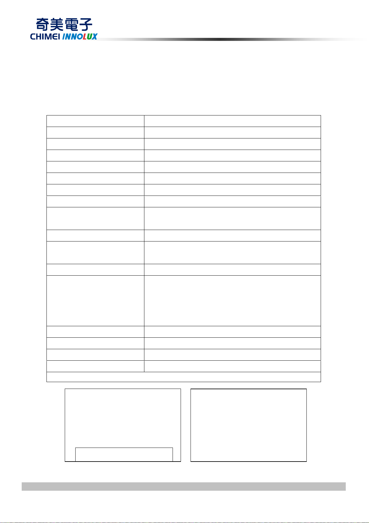
1.3 MECHANICAL SPECIFICATIONS
Item Min. Typ. Max. Unit Note
Weight - 3560 - g -
I/F connector mounting position
Note (1) Please refer to the attached drawings for more information of front and back outline dimensions.
Note (2) Connector mounting position
The mounting inclination of the connector makes the
screen center within ± 0.5mm as the horizontal.
+/- 0.5mm
(2)
Version 2.0 6 Date :Jun.20 2013
The copyright belongs to CHIMEI InnoLux. Any unauthorized use is prohibited
Page 7
PRODUCT SPECIFICATION
2. ABSOLUTE MAXIMUM RATINGS
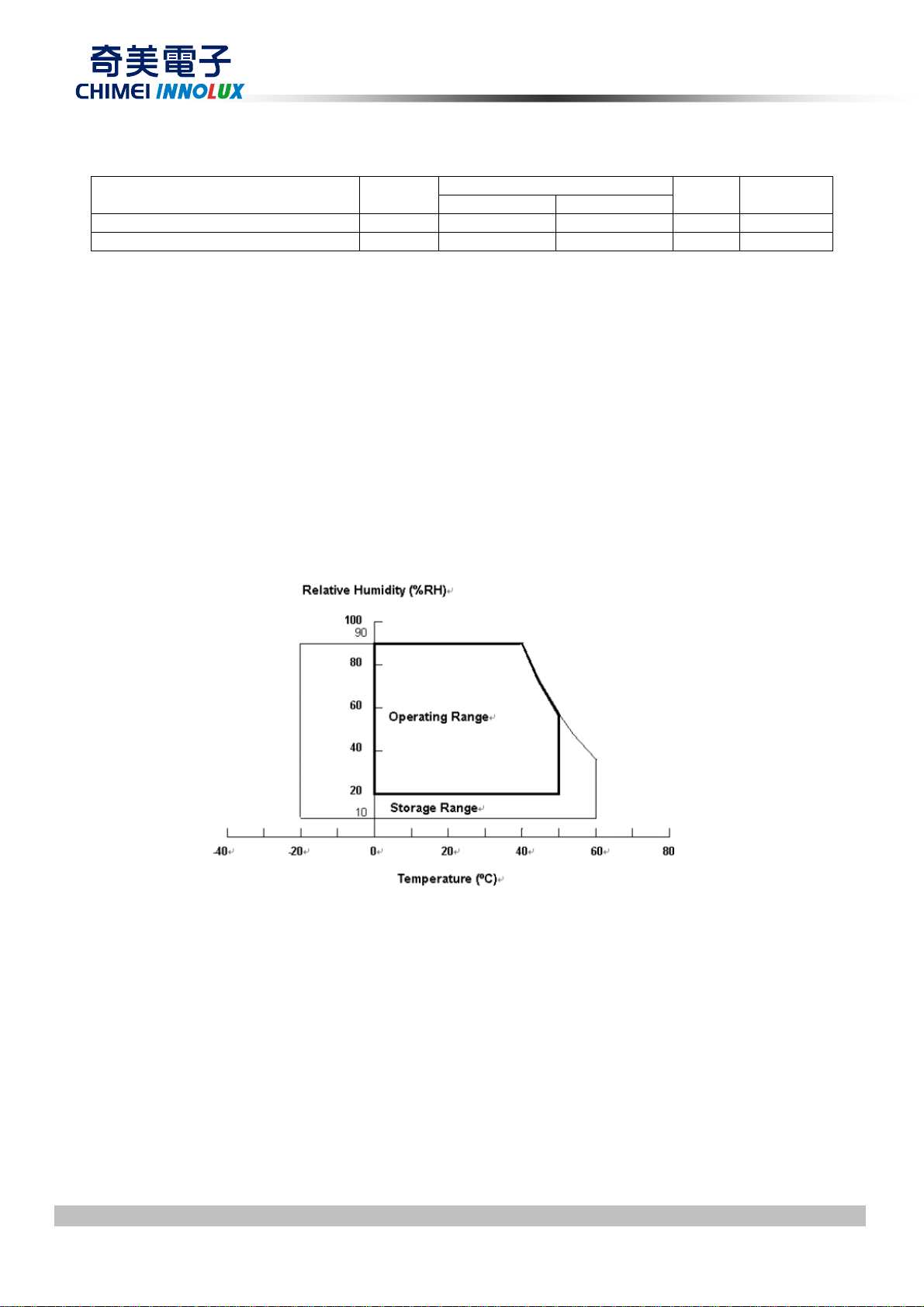
2.1 ABSOLUTE RATINGS OF ENVIRONMENT
Item Symbol
Storage Temperature TST -20 +60 ºC (1), (3)
Operating Ambient Temperature TOP 0 50 ºC (1), (2), (3)
Note (1) Temperature and relative humidity range is shown in the figure below.
(a) 90 %RH Max. (Ta 40 ºC).≦
(b) Wet-bulb temperature should be 39 ºC Max. (Ta > 40 ºC).
(c) No condensation.
Note (2) Thermal management should be considered in final product design to prevent the surface temperature of display
area from being over 65 ºC. The range of operating temperature may degrade in case of improper thermal
management in final product design.
Note (3) The rating of environment is base on LCD module. Leave LCD cell alone, this environment condition can’t be
guaranteed. Except LCD cell, the customer has to consider the ability of other parts of LCD module and LCD module
process.
Min. Max.
Value
Unit Note
Version 2.0 7 Date :Jun.20 2013
The copyright belongs to CHIMEI InnoLux. Any unauthorized use is prohibited
Page 8
PRODUCT SPECIFICATION
2.2 ABSOLUTE RATINGS OF ENVIRONMENT (OPEN CELL)
Recommended Storage Condition: With shipping package.
Recommended Storage temperature range: 25±5 ℃
Recommended Storage humidity range: 50±10%RH
Recommended Shelf life: a month
2.3 ELECTRICAL ABSOLUTE RATINGS
2.3.1 TFT LCD MODULE
Value
Item Symbol
Min. Max.
Power Supply Voltage VCC -0.3 13.5 V
Logic Input Voltage VIN -0.3 3.6 V
Note (1) Permanent damage to the device may occur if maximum values are exceeded. Function operation
Unit Note
(1)
should be restricted to the conditions described under Normal Operating Conditions.
Version 2.0 8 Date :Jun.20 2013
The copyright belongs to CHIMEI InnoLux. Any unauthorized use is prohibited
Page 9
PRODUCT SPECIFICATION
3. ELECTRICAL CHARACTERISTICS
3.1 TFT LCD Module
(Ta = 25 ± 2 ºC)
Value
Parameter Symbol
Min. Typ. Max.
Power Supply Voltage VCC 10.8 12 13.2 V (1)
Unit Note
Rush Current I
White Pattern
OFHD 120Hz Output
Horizontal Stripe
Power Consumption
Black Pattern
White Pattern
OFHD 120Hz Output
Horizontal Stripe
Power Supply Current
Black Pattern
White Pattern
QFHD 60Hz Output
Horizontal Stripe
Power Consumption
Black Pattern
White Pattern
QFHD 60Hz Output
Horizontal Stripe
Power Supply Current
Black Pattern
RUSH
- -
- -
- -
- -
- -
- -
- -
- -
- -
- -
- -
- -
- -
14.4 17.52
28.2 34.08
14.4 17.52
1.2 1.46
2.35 2.84
1.2 1.46
13.44
13.92 16.08
12.96 15.48
1.12 1.38
1.16 1.34
1.08 1.29
3.9
16.56
A (2)
W
W
W
A
A
A
(3)
W
W
W
A
A
A
Differential Input High
Threshold Voltage
Differential Input Low
Threshold Voltage
V
V
LVTH
LVTL
+100
-300
-
-
+300 mV
-100 mV
LVDS
Common Input Voltage VCM 1.0 1.2 1.4 V
(4)
interface
CMOS
interface
Differential input voltage
(single-end)
Terminating Resistor RT
| 200
|V
ID
-
Input High Threshold Voltage VIH 2.7
Input Low Threshold Voltage V
0
IL
-
100
-
-
600 mV
-
ohm
3.3 V
0.7 V
Note (1) The module should be always operated within the above ranges.
Note (2) The ripple voltage should be controlled under 10% of Vcc (Typ.).
Note (3) Measurement condition:
Version 2.0 9 Date :Jun.20 2013
The copyright belongs to CHIMEI InnoLux. Any unauthorized use is prohibited
Page 10
PRODUCT SPECIFICATION
Vcc rising time is 470us
Vcc
0.9Vcc
0.1Vcc
Note (4) The specified power supply current is under the conditions at Vcc = 12 V, Ta = 25 ± 2 ºC, fv = 60/120 Hz
whereas a power dissipation check pattern below is displayed.
a. White Pattern
Active Area
GND
470us
b. Black Pattern
Active Area
c. Horizontal Pattern
R G B R G B R G B
R G BR G B R G BR G B R G BR G B
R G B R G B R G B
R G BR G B R G BR G B R G BR G B
R G B R G B R G B
R G B R G B R G BR G B R G B R G B
R G B R G B R G B
R G B R G B R G BR G B R G B R G B
R G B R G B R G B
R G BR G B R G BR G B R G BR G B
R G B R G B R G B
R G BR G B R G BR G B R G BR G B
Version 2.0 10 Date :Jun.20 2013
The copyright belongs to CHIMEI InnoLux. Any unauthorized use is prohibited
Page 11
Note (5) The LVDS input characteristics are as follows :
PRODUCT SPECIFICATION
Version 2.0 11 Date :Jun.20 2013
The copyright belongs to CHIMEI InnoLux. Any unauthorized use is prohibited
Page 12
4. BLOCK DIAGRAM OF INTERFACE
4.1 TFT LCD MODULE
PRODUCT SPECIFICATION
OUTPUT CONNECTOR
L/R_O
CON2: LM123S-010-H-TF1-3,
INPUT CONNECTOR
CNF1: WF23-400-513C, FCN,
TFT LCD PANEL
(3840x3x2160)
XRR Board XRL Board XLR Board XLL Board
or equivalent
or equivalent
C Board
INPUT CONNECTOR
CNF2: WF23-400-413C,
FCN, or equivalent
CH1_0(+/-)
CH1_1(+/-)
CH1_2(+/-)
CH1_3(+/-)
CH1_4(+/-)
CH1_CLK(+/-)
CH2_0(+/-)
CH2_1(+/-)
CH2_2(+/-)
CH2_3(+/-)
CH2_4(+/-)
CH2_CLK(+/-)
SELLVDS
2D/3D
SCL
SDA
GND
L/R
LD_EN VCC L/R_O
CH3_0(+/-)
CH3_1(+/-)
CH3_2(+/-)
CH3_3(+/-)
CH3_4(+/-)
CH3_CLK(+/-)
CH4_0(+/-)
CH4_1(+/-)
CH4_2(+/-)
CH4_3(+/-)
CH4_4(+/-)
CH4_CLK(+/-)
Version 2.0 12 Date :Jun.20 2013
The copyright belongs to CHIMEI InnoLux. Any unauthorized use is prohibited
Page 13
5. INPUT TERMINAL PIN ASSIGNMENT
5.1 TFT LCD OPEN CELL
CNF1 Connector pin assignment: (WF23-400-513C (FCN ) or equivalent)
PRODUCT SPECIFICATION
Pin Name Description
1 N.C. No Connection (1)
2 SCL I2C Clock (for mode selection & function setting)
3 SDA I2C Data (for mode selection & function setting)
4 N.C. No Connection
5 L/R_O Output signal for Left Right Glasses control
6 N.C. No Connection (1)
7 SELLVDS Input signal for LVDS Data Format Selection (3)(9)
8 N.C. No Connection
9 N.C. No Connection
10 N.C. No Connection
11 GND Ground
12 CH1[0]- First pixel Negative LVDS differential data input. Pair 0
13 CH1[0]+ First pixel Positive LVDS differential data input. Pair 0
Note
(1)
(2)
(1)
14 CH1[1]- First pixel Negative LVDS differential data input. Pair 1
(4)
15 CH1[1]+ First pixel Positive LVDS differential data input. Pair 1
16 CH1[2]- First pixel Negative LVDS differential data input. Pair 2
17 CH1[2]+ First pixel Positive LVDS differential data input. Pair 2
18 GND Ground
19 CH1CLK- First pixel Negative LVDS differential clock input.
20 CH1CLK+ First pixel Positive LVDS differential clock input.
21 GND Ground
22 CH1[3]- First pixel Negative LVDS differential data input. Pair 3
23 CH1[3]+ First pixel Positive LVDS differential data input. Pair 3
24 CH1[4]- First pixel Negative LVDS differential data input. Pair 4
25 CH1[4]+ First pixel Positive LVDS differential data input. Pair 4
26 2D/3D Input signal for 2D/3D Mode Selection (5)(10)
27 L/R Input signal for Left Right eye frame synchronous (6)
(4)
(4)
28 CH2[0]- Second pixel Negative LVDS differential data input. Pair 0
(4)
Version 2.0 13 Date :Jun.20 2013
The copyright belongs to CHIMEI InnoLux. Any unauthorized use is prohibited
Page 14
PRODUCT SPECIFICATION
29 CH2[0]+ Second pixel Positive LVDS differential data input. Pair 0
30 CH2[1]- Second pixel Negative LVDS differential data input. Pair 1
31 CH2[1]+ Second pixel Positive LVDS differential data input. Pair 1
32 CH2[2]- Second pixel Negative LVDS differential data input. Pair 2
33 CH2[2]+ Second pixel Positive LVDS differential data input. Pair 2
34 GND Ground
35 CH2CLK- Second pixel Negative LVDS differential clock input.
36 CH2CLK+ Second pixel Positive LVDS differential clock input.
37 GND Ground
38 CH2[3]- Second pixel Negative LVDS differential data input. Pair 3
39 CH2[3]+ Second pixel Positive LVDS differential data input. Pair 3
40 CH2[4]- Second pixel Negative LVDS differential data input. Pair 4
41 CH2[4]+ Second pixel Positive LVDS differential data input. Pair 4
42 LD_EN Input signal for Local Dimming Enable (7)(9)
43 N.C. No Connection (8)
44 GND Ground
45 GND Ground
46 GND Ground
47 N.C. No Connection
(4)
(4)
(1)
48 VCC +12V power supply
49 VCC +12V power supply
50 VCC +12V power supply
51 VCC +12V power supply
Version 2.0 14 Date :Jun.20 2013
The copyright belongs to CHIMEI InnoLux. Any unauthorized use is prohibited
Page 15

PRODUCT SPECIFICATION
CNF2 Connector pin assignment (WF23-400-413C (FCN) or equivalent)
Pin Name Description Note
1 N.C. No Connection
2 N.C. No Connection
3 N.C. No Connection
4 N.C. No Connection
5 N.C. No Connection
6 N.C. No Connection
7 N.C. No Connection
8 N.C. No Connection
9 GND Ground
10 CH3[0]- Third pixel Negative LVDS differential data input. Pair 0
(1)
11 CH3[0]+ Third pixel Positive LVDS differential data input. Pair 0
12 CH3[1]- Third pixel Negative LVDS differential data input. Pair 1
(4)
13 CH3[1]+ Third pixel Positive LVDS differential data input. Pair 1
14 CH3[2]- Third pixel Negative LVDS differential data input. Pair 2
15 CH3[2]+ Third pixel Positive LVDS differential data input. Pair 2
16 GND Ground
17 CH3CLK- Third pixel Negative LVDS differential clock input.
(4)
18 CH3CLK+ Third pixel Positive LVDS differential clock input.
19 GND Ground
20 CH3[3]- Third pixel Negative LVDS differential data input. Pair 3
21 CH3[3]+ Third pixel Positive LVDS differential data input. Pair 3
(4)
22 CH3[4]- Third pixel Negative LVDS differential data input. Pair 4
23 CH3[4]+ Third pixel Positive LVDS differential data input. Pair 4
24 GND Ground
25 GND Ground
26 CH4[0]- Fourth pixel Negative LVDS differential data input. Pair 0
27 CH4[0]+ Fourth pixel Positive LVDS differential data input. Pair 0
28 CH4[1]- Fourth pixel Negative LVDS differential data input. Pair 1
29 CH4[1]+ Fourth pixel Positive LVDS differential data input. Pair 1
30 CH4[2]- Fourth pixel Negative LVDS differential data input. Pair 2
(4)
Version 2.0 15 Date :Jun.20 2013
The copyright belongs to CHIMEI InnoLux. Any unauthorized use is prohibited
Page 16

PRODUCT SPECIFICATION
L Right glass turn on
H Left glass turn on
31 CH4[2]+ Fourth pixel Positive LVDS differential data input. Pair 2
32 GND Ground
33 CH4CLK- Fourth pixel Negative LVDS differential clock input.
34 CH4CLK+ Fourth pixel Positive LVDS differential clock input.
35 GND Ground
36 CH4[3]- Fourth pixel Negative LVDS differential data input. Pair 3
37 CH4[3]+ Fourth pixel Positive LVDS differential data input. Pair 3
38 CH4[4]- Fourth pixel Negative LVDS differential data input. Pair 4
39 CH4[4]+ Fourth pixel Positive LVDS differential data input. Pair 4
40 GND Ground
41 GND Ground
(4)
(4)
CON2 Connector Pin Assignment LM123S010HTF13Y
1 N.C. No Connection
2 N.C. No Connection
3 N.C. No Connection
4 GND Ground
5 N.C. No Connection
6 L/R_O Output signal for Left Right Glasses control
7 N.C. No Connection
8 N.C. No Connection
9 N.C. No Connection
10 N.C. No Connection
Note (1) Reserved for internal use. Please leave it open.
Note (2) The definition of L/R_O signal as follows
(1)
(1)
(2)
(1)
Version 2.0 16 Date :Jun.20 2013
L= 0V , H= +3.3V
L/R_O Note
The copyright belongs to CHIMEI InnoLux. Any unauthorized use is prohibited
Page 17

Note (3) LVDS format selection.
SELLVDS
Note
L JEIDA Format
H or Open
VESA Format
2D/3D
Note
L or Open
2D Mode
H 3D Mode
L/R Note
L Right synchronous signal
H Left synchronous signal
L= Connect to GND, H=Connect to +3.3V or Open
Note (4) LVDS 4-port Data Mapping
FHD 100/120Hz Input
PRODUCT SPECIFICATION
Port Channel of LVDS
1st Port First Pixel 1, 5, 9, ……1913, 1917
2nd Port Second Pixel
3rd Port Third Pixel 3, 7, 11, ….1915, 1919
4th Port Fourth Pixel 4, 8, 12, ….1916, 1920
QFHD 24/30 Input
Port Channel of LVDS
1st Port First Pixel 1, 5, 9, ……3833, 3837
2nd Port Second Pixel
3rd Port Third Pixel 3, 7, 11, ….3835, 3839
4th Port Fourth Pixel 4, 8, 12, ….3836, 3840
Note (5) 2D/3D mode selection.
L= Connect to GND or Open, H=Connect to +3.3V
Data Stream
2, 6, 10, ….1914, 1918
Data Stream
2, 6, 10, ….3834, 3838
Note (6) Input signal for left and right eye frame synchronous
VIL=0~0.7 V, VIH=2.7~3.3 V
Version 2.0 17 Date :Jun.20 2013
The copyright belongs to CHIMEI InnoLux. Any unauthorized use is prohibited
Page 18

PRODUCT SPECIFICATION
L Local Dimming Dis
able
H or Open
Local Dimming Enable
IC
10
K ohm
1K ohm
Panel Board
System Board
3.3V
Note (7) Local dimming enable selection.
L= Connect to GND,H=Connect to +3.3V or Open
LD_EN Note
Note (8) Reserved for internal use. Open is preferred. However, it is also acceptable to reserve the wire
connecting with specific High/Low voltage level.
Note (9) Interface optional pin has internal scheme as following diagram. Customer should keep the interface
voltage level requirement which including panel board loading as below.
Interface Voltage Level
VH > V
VL < V
IH
IL
Version 2.0 18 Date :Jun.20 2013
The copyright belongs to CHIMEI InnoLux. Any unauthorized use is prohibited
Page 19

PRODUCT SPECIFICATION
IC
10
K ohm
1K ohm
Panel Boar
d System Board
Note (10) Interface optional pin has internal scheme as following diagram. Customer should keep the interface
voltage level requirement which including panel board loading as below.
Interface Voltage Level
VH > V
VL < V
IH
IL
Version 2.0 19 Date :Jun.20 2013
The copyright belongs to CHIMEI InnoLux. Any unauthorized use is prohibited
Page 20

PRODUCT SPECIFICATION
Note (11) LVDS connector pin order defined as follows
Note (12) LVDS connector mating dimension range request is 0.93mm~1.0mm as follow
Note (13) The screw hole which is distant from the connector is merged with Ground
Version 2.0 20 Date :Jun.20 2013
The copyright belongs to CHIMEI InnoLux. Any unauthorized use is prohibited
Page 21

5.2 LVDS INTERFACE
JEIDA Format : SELLVDS = L
VESA Format : SELLVDS = H or Open
PRODUCT SPECIFICATION
R0~R9: Pixel R Data (9; MSB, 0; LSB)
G0~G9: Pixel G Data (9; MSB, 0; LSB)
B0~B9: Pixel B Data (9; MSB, 0; LSB)
DE : Data enable signal
DCLK : Data clock signal
Notes: (1) RSVD (reserved) pins on the transmitter shall be “H” or “L”.
Version 2.0 21 Date :Jun.20 2013
The copyright belongs to CHIMEI InnoLux. Any unauthorized use is prohibited
Page 22

PRODUCT SPECIFICATION
R8 R7 R6 R5 R4 R3 R2 R1 R0 G9 G8 G7 G6 G5 G4 G3 G2 G1 G0 B9 B8 B7 B6 B5 B4 B3 B2 B1 B0
5.3 COLOR DATA INPUT ASSIGNMENT
The brightness of each primary color (red, green and blue) is based on the 10-bit gray scale data input for the color.
The higher the binary input the brighter the color. The table below provides the assignment of color versus data
input.
Data Signal
Color
R9
0
0
1
1
0
0
0
0
0
0
1
1
1
1
1
1
0
0
0
0
0
0
1
1
1
1
1
1
0
0
0
0
0
0
:
:
:
:
0
0
0
0
0
0
0
0
0
0
0
0
:
:
:
:
0
0
0
0
0
0
Basic
Colors
Gray
Scale
Of
Red
Gray
Scale
Of
Green
Gray
Scale
Of
Blue
Black
Red
Green
Blue
Cyan
Magenta
Yellow
White
Red (0) / Dark
Red (1)
Red (2)
:
:
Red (1021)
Red (1022)
Red (1023)
Green (0) / Dark
Green (1)
Green (2)
:
:
Green (1021)
Green (1022)
Green (1023)
Blue (0) / Dark
Blue (1)
Blue (2)
:
:
Blue (1021)
Blue (1022)
Blue (1023)
Note (1) 0: Low Level Voltage,1: High Level Voltage
Red Green Blue
0
0
0
0
0
0
0
0
0
0
0
0
0
0
0
0
0
0
1
1
1
1
1
1
1
1
0
0
0
0
0
0
0
0
0
0
0
0
0
0
0
1
1
1
1
0
0
0
0
0
0
0
0
0
0
0
0
0
0
0
1
1
1
1
1
0
0
0
:
:
1
1
1
0
0
0
:
:
0
0
0
0
0
0
:
:
0
0
0
1
1
1
1
1
1
1
0
0
0
0
0
0
0
0
0
:
:
:
:
:
:
1
1
1
1
1
1
1
1
1
0
0
0
0
0
0
0
0
0
:
:
:
:
:
:
0
0
0
0
0
0
0
0
0
0
0
0
0
0
0
0
0
0
:
:
:
:
:
:
0
0
0
0
0
0
0
0
0
0
1
1
1
1
1
1
1
1
1
0
0
0
0
0
0
0
0
1
:
:
:
:
:
:
1
1
0
1
1
1
1
1
1
0
0
0
0
0
0
0
0
0
:
:
:
:
:
:
0
0
0
0
0
0
0
0
0
0
0
0
0
0
0
0
0
0
:
:
:
:
:
:
0
0
0
0
0
0
0
0
0
0
0
1
1
1
0
0
1
1
1
1
1
1
0
0
0
1
0
0
0
0
0
:
:
:
:
:
:
1
0
0
0
0
0
1
0
0
0
0
0
0
0
0
0
0
0
:
:
:
:
:
:
0
1
1
0
1
1
0
1
1
0
0
0
0
0
0
0
0
0
:
:
:
:
:
:
0
0
0
0
0
0
0
0
0
1
0
0
0
1
1
1
0
0
0
1
1
1
1
1
1
0
0
0
0
0
0
0
0
0
:
:
:
:
:
:
0
0
0
0
0
0
0
0
0
0
0
0
0
0
0
0
0
0
:
:
:
:
:
:
1
1
1
1
1
1
1
1
1
0
0
0
0
0
0
0
0
0
:
:
:
:
:
:
0
0
0
0
0
0
0
0
0
0
1
1
1
0
0
0
1
1
1
0
0
0
1
1
1
1
1
1
0
0
0
0
0
0
0
0
0
:
:
:
:
:
:
0
0
0
0
0
0
0
0
0
0
0
0
0
0
0
0
0
0
:
:
:
:
:
:
1
1
1
1
1
1
1
1
1
0
0
0
0
0
0
0
0
0
:
:
:
:
:
:
0
0
0
0
0
0
0
0
0
0
0
0
0
1
1
0
0
0
1
1
1
1
0
0
1
1
1
0
1
1
1
0
0
0
0
0
0
0
0
0
:
:
:
:
:
;
0
0
0
0
0
0
0
0
0
0
0
0
0
1
0
1
0
0
:
:
:
:
:
:
0
1
0
1
0
0
1
1
0
0
0
0
0
0
0
0
0
0
:
:
:
:
:
:
0
0
1
0
0
1
0
0
1
0
0
0
0
0
0
0
0
0
0
0
1
1
1
1
1
1
1
1
1
0
0
0
1
1
1
0
0
0
0
0
0
0
0
0
:
:
:
:
:
:
0
0
0
0
0
0
0
0
0
0
0
0
0
0
0
0
0
0
:
:
:
:
:
:
0
0
0
0
0
0
0
0
0
0
0
0
0
0
0
0
0
0
:
:
:
:
:
:
1
1
1
1
1
1
1
1
1
0
0
0
0
0
0
0
1
1
1
1
1
1
1
1
1
0
0
0
1
1
1
0
0
0
0
0
0
0
0
0
:
:
:
:
:
:
0
0
0
0
0
0
0
0
0
0
0
0
0
0
0
0
0
0
:
:
:
:
:
:
0
0
0
0
0
0
0
0
0
0
0
0
0
0
0
0
0
0
:
:
:
:
:
:
1
1
1
1
1
1
1
1
1
0
0
0
0
0
0
0
0
0
1
1
1
1
1
1
1
1
1
0
0
0
1
1
1
0
0
0
0
0
0
0
0
0
:
:
:
:
:
:
0
0
0
0
0
0
0
0
0
0
0
0
0
0
0
0
0
0
:
:
:
:
:
:
0
0
0
0
0
0
0
0
0
0
0
0
0
0
1
0
1
0
:
:
:
:
:
:
1
0
1
1
1
0
1
1
1
Version 2.0 22 Date :Jun.20 2013
The copyright belongs to CHIMEI InnoLux. Any unauthorized use is prohibited
Page 23

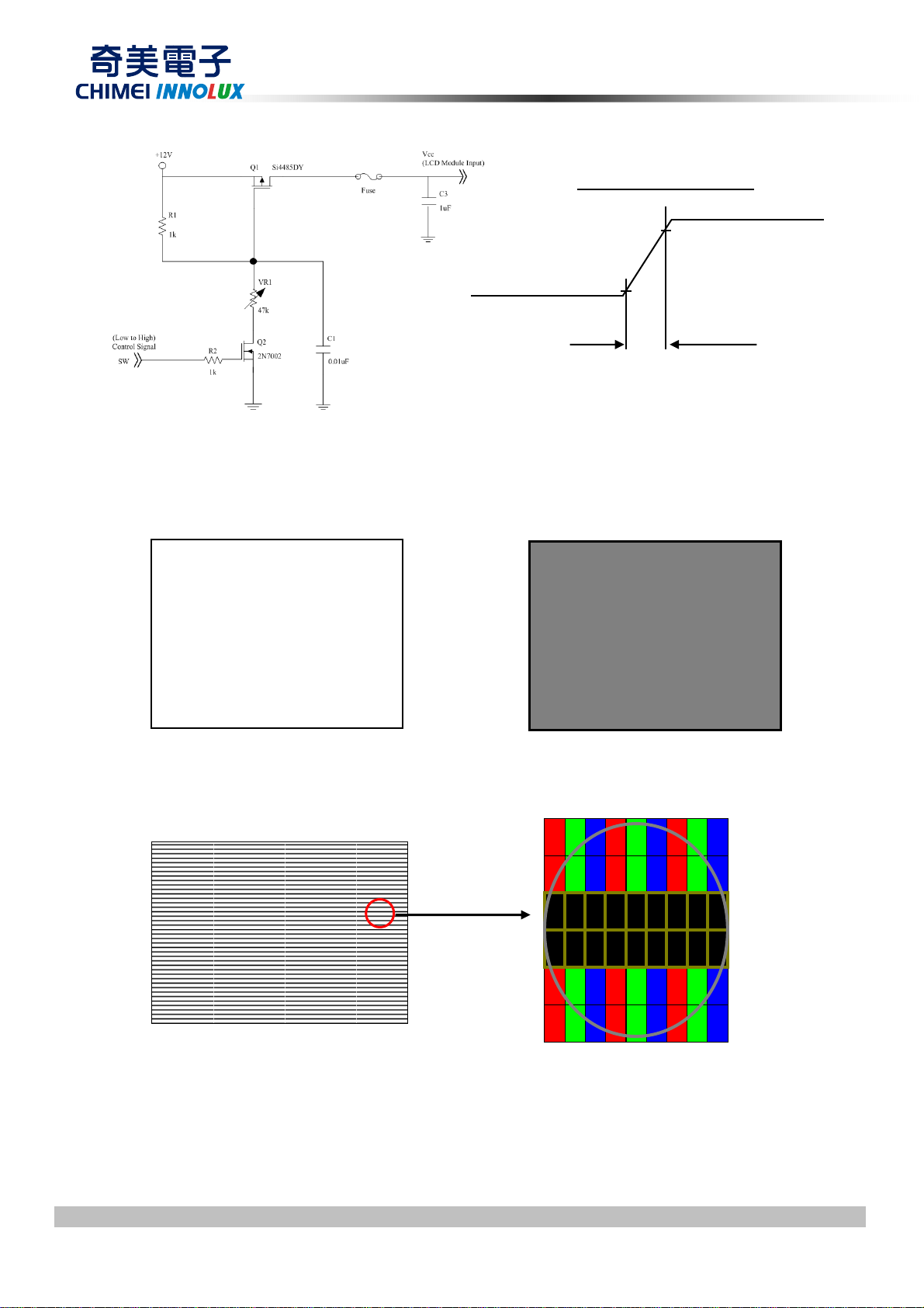
5.4 FLICKER (Vcom) ADJUSTMENT
(1) Adjustment Pattern:
The adjustment pattern is shown as below. If customer needs below pattern, please directly contact with
CMI account FAE.
Frame N Frame N+1
PRODUCT SPECIFICATION
(2) Adjustment method: (Digital V-com)
Programmable memory IC is used for Digital V-com adjustment in this model. CMI provide auto Vcom tools to
adjust Digital V-com. The detail connection and setting instruction, please directly contact with account FAE or
refer to CMI auto V-com adjustment O.I. Below items is suggested to be ready before Digital V-com
adjustment in customer LCM line.
a. USB Sensor Board.
b. Programmable software
c. Document: Auto V-com adjustment suggestion O.I.
Version 2.0 23 Date :Jun.20 2013
The copyright belongs to CHIMEI InnoLux. Any unauthorized use is prohibited
Page 24

PRODUCT SPECIFICATION
6. INTERFACE TIMING
6.1 INPUT SIGNAL TIMING SPECIFICATIONS
(Ta = 25 ± 2 ºC)
The input signal timing specifications are shown as the following table and timing diagram.
Signal Item Symbol
Min. Typ. Max. Unit Note
Input cycle to
T
- - 200 ps (1)
cycle jitter
rcl
LVDS
Spread spectrum
Receiver
modulation range
clkin_mod
F
F
clkin
-1.5%
- F
+1.5% MHz
clkin
Clock
Spread spectrum
modulation frequency
F
SSM
- - 66 KHz
LVDS
Receiver
Receiver skew margin T
RSKM
-400 - 400 ps (3)
Data
6.1.1 Input Timing SPEC for FHD, Frame Rate = 100Hz
Signal Item Symbol
LVDS Clock Frequency
F
clkin
(=1/TC)
Min. Typ. Max. Unit Note
60 74.25 79 MHz (4)
Frame Rate 2D Mode Fr 97 100 103 Hz (5)
(2)
Total Tv 1104 1350 1395 Th Tv=Tvd+Tvb
Vertical
Active
Display
Display Tvd 1080 Th
Blank Tvb 24 270 315 Th
Front porch Tvfp 10
- -
Th
Term
Back porch Tvbp
Vsync Tvswid
10
4
- -
- -
Th
Th
(6)
2D Mode
Total Th 530 550 670 Tc Th=Thd+Thb
Horizontal
Active
Display
Term
Display Thd 480 Tc
Blank Thb 50 70 190 Tc
Front porch Thfp 5
Back porch Thbp
Hsync Thswid
5
2
- -
- -
- -
Tc
Tc
Tc
(6)
Version 2.0 24 Date :Jun.20 2013
The copyright belongs to CHIMEI InnoLux. Any unauthorized use is prohibited
Page 25

6.1.2 Input Timing SPEC for FHD, Frame Rate = 120Hz
PRODUCT SPECIFICATION
Signal Item Symbol
2D Mode 60 74.25 79 MHz
LVDS Clock
3D Mode
2D Mode 117 120 123 Hz
Frame Rate
3D Mode
Total Tv 1104 1125 1395 Th Tv=Tvd+Tvb
Display Tvd 1080 Th
Blank Tvb 24 45 315 Th
2D Mode
Front porch Tvfp 10
Vertical
Active
Display
Term
Back porch Tvbp
Vsync Tvswid
Total Tv 1125 Th
Display Tvd 1080 Th
F
clkin
(=1/TC
Fr
Min. Typ. Max. Unit Note
(4)
74.25 MHz
(5)
120 Hz
10
4
- -
- -
- -
Th
Th
Th
(6)
Horizontal
Active
Display
Term
3D Mode
2D Mode
3D Mode
Blank Tvb 45 Th
Front porch Tvfp 10
Back porch Tvbp
Vsync Tvswid
Total Th 530 550 670 Tc Th=Thd+Thb
Display Thd 480 Tc
Blank Thb 50 70 190 Tc
Front porch Thfp 5
Back porch Thbp
Hsync Thswid
Total Th 530 550 670 Tc Th=Thd+Thb
Display Thd 480 Tc
Blank Thb 50 70 190 Tc
Front porch Thfp 5
10
4
5
2
- - -
- - -
- - -
- -
- -
- -
- -
Tc
Tc
Tc
Tc
(6)
(6)
Back porch Thbp
Hsync Thswid
5
2
- -
- -
Tc
Tc
(6)
Version 2.0 25 Date :Jun.20 2013
The copyright belongs to CHIMEI InnoLux. Any unauthorized use is prohibited
Page 26

6.1.3 Input Timing SPEC for QFHD, Frame Rate = 24Hz
PRODUCT SPECIFICATION
Signal Item Symbol
F
LVDS Clock Frequency
Frame Rate 2D Mode Fr 23 24 25 Hz (5)
Total Tv 2208 2250 2450 Th Tv=Tvd+Tvb
Vertical
Active
Display
Term
2D Mode
Horizontal
Active
Display Tvd 2160 Th
Blank Tvb 48 90 290 Th
Front porch Tvfp 20
Back porch Tvbp
Vsync Tvswid
Total Th 990 1375 1440 Tc Th=Thd+Thb
Display Thd 960 Tc
Blank Thb 30 415 480 Tc
clkin
(=1/TC)
Min. Typ. Max. Unit Note
60 74.25 79 MHz (4)
20
8
- -
- -
- -
Th
Th
Th
(6)
Display
Term
Front porch Thfp 10
Back porch Thbp
Hsync Thswid
10
4
- -
- -
- -
Tc
Tc
Tc
(6)
Version 2.0 26 Date :Jun.20 2013
The copyright belongs to CHIMEI InnoLux. Any unauthorized use is prohibited
Page 27

6.1.4 Input Timing SPEC for QFHD, Frame Rate = 30Hz
PRODUCT SPECIFICATION
Signal Item Symbol
F
LVDS Clock Frequency
Frame Rate 2D Mode Fr 29 30 31 Hz (5)
Total Tv 2208 2250 2450 Th Tv=Tvd+Tvb
Vertical
Active
Display
Term
2D Mode
Horizontal
Active
Display Tvd 2160 Th
Blank Tvb 48 90 290 Th
Front porch Tvfp 20
Back porch Tvbp
Vsync Tvswid
Total Th 992 1100 1340 Tc Th=Thd+Thb
Display Thd 960 Tc
Blank Thb
clkin
(=1/TC)
Min. Typ. Max. Unit Note
60 74.25 79 MHz (4)
20
8
32
- -
- -
- -
140 380 Tc
Th
Th
Th
(6)
Display
Term
Note (1) The input clock cycle-to-cycle jitter is defined as below figures. Trcl =|T1 – T︱
Front porch Thfp
Back porch Thbp
Hsync Thswid
12
10
4
- -
- -
- -
Tc
Tc
Tc
(6)
Version 2.0 27 Date :Jun.20 2013
The copyright belongs to CHIMEI InnoLux. Any unauthorized use is prohibited
Page 28

PRODUCT SPECIFICATION
Note (2) The SSCG (Spread spectrum clock generator) is defined as below figures.
Note (3) The LVDS timing diagram and the receiver skew margin is defined and shown in following figure.
RXCLK+/-
RXn+/-
T
RSKM
Note (4) Please make sure the range of pixel clock has follow the below equation.
Tc
Fclkin(max) ≧ (Fr Tv Th╳ ╳ ) Fclkin(min)≧
Version 2.0 28 Date :Jun.20 2013
The copyright belongs to CHIMEI InnoLux. Any unauthorized use is prohibited
Page 29

PRODUCT SPECIFICATION
Note (5)
a. The frame-to-frame jitter of the input frame rate is defined as the following figure.
b. FRn = FRn-1 ± 1.8%.
Note (6)
a. Hsync and Vsync signals are necessary for this module.
b. The polarity of Hsync & Vsync should be positive.
c. Please follow the input signal timing diagram as below :
Version 2.0 29 Date :Jun.20 2013
The copyright belongs to CHIMEI InnoLux. Any unauthorized use is prohibited
Page 30

PRODUCT SPECIFICATION
100ms T6≦
T
10≦10ms
6.2 POWER ON/OFF SEQUENCE
(Ta = 25 ± 2 ºC)
To prevent a latch-up or DC operation of LCD module, the power on/off sequence should be as the diagram
below.
0.9VCC
0.9VCC
0V
0.5 T1≦ ≦10ms
0 T2≦ ≦200ms
0 T3≦
500ms T4≦
0.1VCC
T1
T2
0.1VCC
T3
T4
LVDS Signals
0 T7 T2≦ ≦
0 T8≦ ≦T3
0V
Power on
T7
VALID
Power off
T8
Option Signals
(SELLVDS,2D/3D,LD_EN)
T9
500ms T9≦
Host I2C Command
Backlight (Recommended)
1000ms≦T5
T5
50% 50%
T6
Vcc Dip
Vcc
Vcc(typ.) x 0.85
0V
Power ON/OFF Sequence
T10
Version 2.0 30 Date :Jun.20 2013
The copyright belongs to CHIMEI InnoLux. Any unauthorized use is prohibited
Page 31

PRODUCT SPECIFICATION
Note (1) The supply voltage of external system for the module input should follow the definition of Vcc.
Note (2) Apply the lamp voltage within the LCD operation range. When the backlight turns on before the LCD
operation or the LCD turns off before the backlight turns off, the display may momentarily become
abnormal screen.
Note (3) In case of VCC=off, please keep the level of input signals on the low or high impedance.
Note (4) T4 should be measured after the module has been fully discharged between power off and on period.
Note (5) Interface signal shall not be kept at high impedance when the power is on.
Note (6) Vcc must decay smoothly when power-off.
Version 2.0 31 Date :Jun.20 2013
The copyright belongs to CHIMEI InnoLux. Any unauthorized use is prohibited
Page 32

PRODUCT SPECIFICATION
7. OPTICAL CHARACTERISTICS
7.1 TEST CONDITIONS
Item Symbol Value Unit
Ambient Temperature Ta
Ambient Humidity Ha
Supply Voltage VCC
Input Signal According to typical value in "3. ELECTRICAL CHARACTERISTICS"
The LCD module should be stabilized at given temperature for 1 hour to avoid abrupt temperature change during
measuring in a windless room.
25±2
50±10
12V±1.2
o
C
%RH
V
LCD Module
LCD Panel
Field of View = 1º
500 mm
CS - 2000
Light Shield Room
(Ambient Luminance < 2 lux)
Version 2.0 32 Date :Jun.20 2013
The copyright belongs to CHIMEI InnoLux. Any unauthorized use is prohibited
Page 33

PRODUCT SPECIFICATION
7.2 OPTICAL SPECIFICATIONS
The relative measurement methods of optical characteristics are shown as below. The following items should
be measured under the test conditions described in 7.1 and stable environment shown in 7.1.
Item Symbol
Color
Chromaticity
Red
Green
Blue
Rcx
Rcy
Gcx
Gcy
Bcx
Bcy
Wcx
Viewing Angle at Normal
Standard light source “C”
Condition Min. Typ. Max. Unit Note
0.654
0.325
0.272
-
-
-
=0°, θY =0°
θ
x
Direction
Typ.
-0.03
0.587
0.135
0.110
0.300
Typ.
+0.03
-
-
-
-
(0)
White
Wcy
-
0.354
Center Transmittance T% 3.68 4.09 % (5)
=0°, θY =0°
θ
Transmittance Variation
δT
x
1.3 (6)
with CMI module
Contrast Ratio CR
Gray to
Response Time
gray
=0°, θY =0°
θ
x
with CMI Module
3500 5000
- 6.5 13 ms
- - (1),(3)
(1),(4)
θ
+
x
80
88
-
Horizontal
Viewing
θ
-
x
CR≥20
80
88
Deg.
Angle
θ
+
Y
With CMI module
80
88
-
Vertical
θ
-
Y
80
88
-
Transmission direction
Φup-P
-
-
90
-
Deg. (7) -
Of the up polarizer
Note (0) Light source is the standard light source ”C” which is defined by CIE and driving voltage are based on
suitable gamma voltages. The calculating method is as following:
1. Measure Module’s and BLU’s spectrum at center point. White and R,G,B are with signal input. BLU (for
V580DK1-LS1) is supplied by INX.
2. Calculate cell’s spectrum.’
3. Calculate cell’s chromaticity by using the spectrum of standard light source “C”.
Note (1) Light source is the BLU which supplied by INX ( V580DK1-LS1) and the cell driving voltage are based on suitable
gamma voltages.
(1),(2)
Version 2.0 33 Date :Jun.20 2013
The copyright belongs to CHIMEI InnoLux. Any unauthorized use is prohibited
Page 34

Note (2) Definition of Viewing Angle (θx, θy) :
Time
Viewing angles are measured by Autronic Conoscope Cono-80 (or Eldim EZ-Contrast 160R)
PRODUCT SPECIFICATION
θX- = 90º
6 o’clock
θy- = 90º
Note (3) Definition of Contrast Ratio (CR):
The contrast ratio can be calculated by the following expression.
y-
x-
Normal
θx = θy = 0º
θy- θy+
θx−
θx+
12 o’clock direction
y+
θy+ = 90º
x+
θX+ = 90º
Contrast Ratio (CR) =
L1023 : Luminance of gray level 1023
L0 : Luminance of gray level 0
CR = CR (5), where CR (X) is corresponding to the Contrast Ratio of the point X at the figure in Note (5).
Note (4) Definition of Gray-to-Gray Switching Time:
Gray Level 1023
100%
90%
Optical
Response
10%
0%
TR
1023 L of Luminance Surface
L0 of Luminance Surface
Gray Level 0
Gray Level 1023
TF
The driving signal means the signal of gray level 0, 124, 252, 380, 508, 636, 764, 892 and 1023.
Gray to gray average time means the average switching time of gray level 0, 124, 252, 380, 508, 636, 764, 892 and
1023 to each other.
Version 2.0 34 Date :Jun.20 2013
The copyright belongs to CHIMEI InnoLux. Any unauthorized use is prohibited
Page 35

Note (5) Definition of Transmittance (T%) :
[
]
Measure the transmittance at 5 points.
Light source is the BLU which contains three diffuser sheets and the cell driving voltage are based on suitable
gamma voltages.
PRODUCT SPECIFICATION
Transmittance (T%) =
The transmittance of each point can be calculated by the following expression.
T (X) =
L255: Luminance of gray level 255
T(X) is corresponding to the point X1~X5 at the figure in Note (6).
Note (6) Definition of Transmittance Variation (δT) :
Measure the transmittance at 5 points.
Transmittance Variation (δT )=
T(X) is calculated as Note(5).
T(5)T(4),T(3),T(2),T(1), Average
module LCD of (X) L255
×
BLU of (X) Luminance
%100
] T(5) T(4), T(3), T(2), T(1), [ Maximum
] T(5) T(4), T(3), T(2), T(1), [ Minimum
Version 2.0 35 Date :Jun.20 2013
The copyright belongs to CHIMEI InnoLux. Any unauthorized use is prohibited
Page 36

PRODUCT SPECIFICATION
6 o’clock
Note (7) This is a reference for designing the shutter glasses of 3D application. (VA case)
Definition of the transmission direction of the up polarizer (Φ
) on LCD Module:
up-P
12 o’clock direction
x-
y-
Φ
up-P
y+
x
+
Φ=0o
Up Polarizer
The transmission axis of the front polarizer of the shutter glasses should be parallel to this panel transmission direction to
get a maximum 3D mode luminance.
Version 2.0 36 Date :Jun.20 2013
The copyright belongs to CHIMEI InnoLux. Any unauthorized use is prohibited
Page 37

PRODUCT SPECIFICATION
8. PRECAUTIONS
8.1 ASSEMBLY AND HANDLING PRECAUTIONS
[ 1 ] Do not apply improper or unbalanced force such as bending or twisting to open cells during assembly.
[ 2 ] It is recommended to assemble or to install an open cell into a customer’s product in clean working areas.
The dust and oil may cause electrical short to an open cell or worsen polarizers on an open cell.
[ 3 ] Do not apply pressure or impulse to an open cell to prevent the damage.
[ 4 ] Always follow the correct power-on sequence when an open cell is assembled and turned on. This can
prevent the damage and latch-up of the CMOS LSI chips.
[ 5 ] Do not design sharp-pointed structure / parting line / tooling gate on the plastic part of a COF (Chip on film),
because the burr will scrape the COF.
[ 6 ] If COF would be bended in assemble process, do not place IC on the bending corner.
[ 7 ] The gap between COF IC and any structure of BLU must be bigger than 2 mm. This can prevent the damage
of COF IC.
[ 8 ] The bezel opening must have no burr and be smooth to prevent the surface of an open cell scraped.
[ 9 ] The bezel of a module or a TV set can not contact with force on the surface of an open cell. It might cause
light leakage or scrape.
[ 10 ] In the case of no FFC or FPC attached with open cells, customers can refer the FFC / FPC drawing and buy
them by self.
[ 11 ] It is important to keep enough clearance between customers’ front bezel/backlight and an open cell.
Without enough clearance, the unexpected force during module assembly procedure may damage an open
cell.
[ 12 ] Do not plug in or unplug an I/F (interface) connector while an assembled open cell is in operation.
[ 13 ] Use a soft dry cloth without chemicals for cleaning, because the surface of the polarizer is very soft and
easily scratched.
[ 14 ] Moisture can easily penetrate into an open cell and may cause the damage during operation.
[ 15 ] When storing open cells as spares for a long time, the following precaution is necessary.
[ 15.1 ] Do not leave open cells in high temperature and high humidity for a long time. It is highly
recommended to store open cells in the temperature range from 0 to 35 at normal humidity without ℃
condensation.
[ 15.2 ] Open cells shall be stored in dark place. Do not store open cells in direct sunlight or fluorescent light
environment.
[ 16 ] When ambient temperature is lower than 10ºC, the display quality might be reduced.
[ 17 ] Unpacking (Cartons/Tray plates) in order to prevent open cells broken:
[ 17.1 ] Moving tray plates by one operator may cause tray plates bent which may induce open cells broken.
Two operators carry one carton with their two hands. Do not throw cartons/tray plates, avoid any
impact on cartons/tray plates, and put down & pile cartons/tray plates gently.
[ 17.2 ] A tray plate handled with unbalanced force may cause an open cell damaged. Trays should be
completely put on a flat platform.
Version 2.0 37 Date :Jun.20 2013
The copyright belongs to CHIMEI InnoLux. Any unauthorized use is prohibited
Page 38

PRODUCT SPECIFICATION
[ 17.3 ] To prevent open cells broken, tray plates should be moved one by one from a plastic bag.
[ 17.4 ] Please follow the packing design instruction, such as the maximum number of tray stacking to
prevent the deformation of tray plates which may cause open cells broken.
[ 17.5 ] To prevent an open cell broken or a COF damaged on a tray, please follow the instructions below:
[17.5.1] Do not peel a polarizer protection film of an open cell off on a tray
[17.5.2] Do not install FFC or LVDS cables of an open cell on a tray
[17.5.3] Do not press the surface of an open cell on a tray.
[17.5.4] Do not pull X-board when an open cell placed on a tray.
[ 18 ] Unpacking (Hard Box) in order to prevent open cells broken:
[ 18.1 ] Moving hard boxes by one operator may cause hard boxes fell down and open cells broken by
abnormal methods. Two operators carry one hard box with their two hands. Do handle hard boxes
carefully, such as avoiding impact, putting down, and piling up gently.
[ 18.2 ] To prevent hard boxes sliding from carts and falling down, hard boxes should be placed on a surface
with resistance.
[ 18.3 ] To prevent an open cell broken or a COF damaged in a hard box, please follow the instructions
below:
[18.3.1] Do not peel a polarizer protection film of an open cell off in a hard box.
[18.3.2] Do not install FFC or LVDS cables of an open cell in a hard box.
[18.3.3] Do not press the surface of an open cell in a hard box.
[18.3.4] Do not pull X-board when an open cell placed in a hard box.
[ 19 ] Handling – In order to prevent open cells, COFs , and components damaged:
[ 19.1 ] The forced displacement between open cells and X-board may cause a COF damaged. Use a fixture
tool for handling an open cell to avoid X-board vibrating and interfering with other components on a
PCBA & a COF.
[ 19.2 ] To prevent open cells and COFs damaged by taking out from hard boxes, using vacuum jigs to take
out open cells horizontally is recommended.
[ 19.3 ] Improper installation procedure may cause COFs of an open cell over bent which causes damages.
As installing an open cell on a backlight or a test jig, place the bottom side of the open cell first on the
backlight or the test jig and make sure no interference before fitting the open cell into the
backlight/the test jig.
[ 19.4 ] Handle open cells one by one.
[ 20 ] Avoid any metal or conductive material to contact PCB components, because it could cause electrical
damage or defect.
8.2 SAFETY PRECAUTIONS
[ 1 ] If the liquid crystal material leaks from the open cell, it should be kept away from the eyes or mouth. In case
of contact with hands, skin or clothes, it has to be washed away thoroughly with soap.
[ 2 ] After the end of life, open cells are not harmful in case of normal operation and storage.
Version 2.0 38 Date :Jun.20 2013
The copyright belongs to CHIMEI InnoLux. Any unauthorized use is prohibited
Page 39

PRODUCT SPECIFICATION
9. DEFINITION OF LABELS
9.1 OPEN CELL LABEL
The barcode nameplate is pasted on each open cell as illustration for CMI internal contro
Figure.9-1 Serial No. Label on SPWB
Model Name : V580DK1-PS1
Revision : Rev. XX, for example: A0, A1… B1, B2… or C1, C2…etc.
Serial ID : X X X X X X X Y M D L N N N N
V580DK1 –PS1
X X X X X X X Y M D L N N N N
Serial No.
Year, Month, Date
CMI Internal Use
Revision
Rev. XX
Serial ID includes the information as below:
Manufactured Date :
Year: 2010=0, 2011=1,2012=2…etc.
Month: 1~9, A~C, for Jan. ~ Dec.
Day: 1~9, A~Y, for 1st to 31st, exclude I ,O, and U.
Revision Code : Cover all the change
Serial No.: Manufacturing sequence of product
CMI Internal Use
Version 2.0 39 Date :Jun.20 2013
The copyright belongs to CHIMEI InnoLux. Any unauthorized use is prohibited
Page 40

TXXXXXXXXXXX
Figure.9-2 Panel ID Label on Cell
Panel ID Label includes the information as below:
Panel ID: T X X X X X X X X X X X
PRODUCT SPECIFICATION
CMI Internal Use
FAB Line: 1~8, for Fab1~Fab8
TFT
Version 2.0 40 Date :Jun.20 2013
The copyright belongs to CHIMEI InnoLux. Any unauthorized use is prohibited
Page 41

10. PACKAGING
10.1 PACKING SPECIFICATIONS
(1) 10 LCD TV PANELS / 1 BOX
(2) BOX DIMENSIONS : 1450 (L) X910 (W) X97.6 (H)mm
(3) WEIGHT : APPROXIMATELY 51.5 Kg ( 10 panels per box)
(4) 80 LCD TV PANELS / 1 GROUP
(5) Without the outer carton, Boxes stack under the package architecture
10.2 PACKING METHOD
Packing method is shown in following Figures 10-1 and 10-2
Figure.10-1 packing method
PRODUCT SPECIFICATION
Version 2.0 41 Date :Jun.20 2013
The copyright belongs to CHIMEI InnoLux. Any unauthorized use is prohibited
Page 42

PRODUCT SPECIFICATION
10.3 UNPACKAGING METHOD
Figure.10-2 packing method
Figures 10-3 are the unpacking method,
Version 2.0 42 Date :Jun.20 2013
The copyright belongs to CHIMEI InnoLux. Any unauthorized use is prohibited
Page 43

11. MECHANICAL CHARACTERISTIC
PRODUCT SPECIFICATION
Version 2.0 43 Date :Jun.20 2013
The copyright belongs to CHIMEI InnoLux. Any unauthorized use is prohibited
Page 44

PRODUCT SPECIFICATION
Version 2.0 44 Date :Jun.20 2013
The copyright belongs to CHIMEI InnoLux. Any unauthorized use is prohibited
 Loading...