

Page 1
Global LCD Panel Exchange Center
g
MODEL NO.: V546HK3
SUFFIX: PS1
www.panelook.com
PRODUCT SPECIFICATION
ϭ
Tentative Specification
ϭ
Preliminary Specification
Ϯ
Approval Specification
ƵƐƚŽŵĞƌ
WWZKsz^/'EdhZ
EĂŵĞdŝƚůĞ
EŽƚĞ
WůĞĂƐĞƌĞƚƵƌŶϭĐŽƉLJĨŽƌLJŽƵƌĐŽŶĨŝƌŵĂƚŝŽŶǁŝƚŚLJŽƵƌ
ƐŝŐŶĂƚƵƌĞĂŶĚĐŽŵŵĞŶƚƐ
Refer to "V546" Incomin
Approved By Checked By Prepared By
Chao-Chun
Chung
Inspection Spe
Ken Wu
c
Yi Chen
Chiang
Version 2.1 1 DateΚΚΚΚ6 Jun. 2012
The copyright belongs to CHIMEI InnoLux. Any unauthorized use is prohibited
One step solution for LCD / PDP / OLED panel application: Datasheet, inventory and accessory!
www.panelook.com
Page 2
Global LCD Panel Exchange Center
www.panelook.com
PRODUCT SPECIFICATION
CONTENTS
1. GENERAL DESCRIPTION ........................................................................................................................................ 5
1.1 OVERVIEW ...................................................................................................................................................... 5
1.2 FEATURES.......................................................................................................................................................5
1.3 MECHANICAL SPECIFICATIONS ................................................................................................................... 5
2. ABSOLUTE MAXIMUM RATINGS ............................................................................................................................6
2.1 ABSOLUTE RATINGS OF ENVIRONMENT .................................................................................................... 6
2.2 ELECTRICAL ABSOLUTE RATINGS(OPEN CELL)........................................................................................7
2.3 ELECTRICAL ABSOLUTE RATINGS .............................................................................................................. 7
3. ELECTRICAL CHARACTERISTICS .........................................................................................................................8
3.1 TFT LCD Module .............................................................................................................................................. 8
4. BLOCK DIAGRAM OF INTERFACE ....................................................................................................................... 11
4.1 TFT LCD MODULE ........................................................................................................................................ 11
5 .INPUT TERMINAL PIN ASSIGNMENT ...................................................................................................................12
5.1 TFT LCD OPEN CELL ...................................................................................................................................12
5.2 LVDS INTERFACE ......................................................................................................................................... 19
5.3 COLOR DATA INPUT ASSIGNMENT ............................................................................................................20
5.4 FLICKER (Vcom/Gamma) ADJUSTMENT.....................................................................................................22
6. INTERFACE TIMING...............................................................................................................................................23
6.1 INPUT SIGNAL TIMING SPECIFICATIONS .................................................................................................. 23
6.1.1 Timing spec for Frame Rate = 100Hz .........................................................................................................23
6.1.2 Timing spec for Frame Rate = 120Hz .........................................................................................................24
6.2 POWER ON/OFF SEQUENCE......................................................................................................................27
7. OPTICAL CHARACTERISTICS ..............................................................................................................................28
7.1 TEST CONDITIONS.......................................................................................................................................28
7.2 OPTICAL SPECIFICATIONS .........................................................................................................................29
8.PRECAUTIONS........................................................................................................................................................32
8.1 ASSEMBLY AND HANDLING PRECAUTIONS .............................................................................................32
8.2 SAFETY PRECAUTIONS ..............................................................................................................................32
9. DEFINITION OF LABELS........................................................................................................................................33
9.1 OPEN CELL LABEL .......................................................................................................................................33
9.2 CARTON LABEL ............................................................................................................................................ 35
10. Packaging ..............................................................................................................................................................36
10.1 PACKING SPECIFICATIONS.......................................................................................................................36
10.2 PACKING METHOD..................................................................................................................................... 36
11. MECHANICAL CHARACTERISTIC....................................................................................................................... 38
Version 2.1 2 DateΚΚΚΚ6 Jun. 2012
The copyright belongs to CHIMEI InnoLux. Any unauthorized use is prohibited
One step solution for LCD / PDP / OLED panel application: Datasheet, inventory and accessory!
www.panelook.com
Page 3

Global LCD Panel Exchange Center
www.panelook.com
PRODUCT SPECIFICATION
Appendix A................................................................................................................................................................... 40
Version 2.1 3 DateΚΚΚΚ6 Jun. 2012
The copyright belongs to CHIMEI InnoLux. Any unauthorized use is prohibited
One step solution for LCD / PDP / OLED panel application: Datasheet, inventory and accessory!
www.panelook.com
Page 4
Global LCD Panel Exchange Center
App
www.panelook.com
PRODUCT SPECIFICATION
REVISION HISTORY
Version Date
Ver 2.1 6 Jun.12 All All
Page
(New)
Section Description
The
roval specification was first issued.
Version 2.1 4 DateΚΚΚΚ6 Jun. 2012
The copyright belongs to CHIMEI InnoLux. Any unauthorized use is prohibited
One step solution for LCD / PDP / OLED panel application: Datasheet, inventory and accessory!
www.panelook.com
Page 5
Global LCD Panel Exchange Center
1. GENERAL DESCRIPTION
1.1 OVERVIEW
V546HK3-PS1 is a 54.6” TFT Liquid Crystal Display product with driver ICs and 4ch-LVDS interface. This
product supports 1920 x 1080 HDTV format and can display true 1.073G colors (10-bit). The backlight unit is
not built in.
1.2 FEATURES
CHARACTERISTICS ITEMS SPECIFICATIONS
Screen Diagonal [in] 54.6
www.panelook.com
PRODUCT SPECIFICATION
Pixels [lines]
Active Area [mm] 1209.6(H) x 680.4(V) (54.6” diagonal)
Sub-Pixel Pitch [mm] 0.21(H) x 0.63(V)
Pixel Arrangement RGB vertical stripe
Weight [g] 3450
Physical Size [mm] 1225.5(W) x696.5(H) x 1.80(D) Typ
Display Mode Transmissive mode / Normally black
Contrast Ratio 6000:1 Typ.
Glass thickness (Array / CF) [mm] 0.7 / 0.7
Viewing Angle (CR>20) +88/-88(H),+88/-88(V) Typ.
Color Chromaticity
1920 1080
(Typical value measured at CMI’s module)
(Typical value measured at CMI’s module)
R=(0.659, 0.324)
G=(0.267, 0.585)
B=(0.133, 0.107)
W=(0.304, 0.361)
* Please refer to “color chromaticity” on p.24
Cell Transparency [%] 6.4%Typ.
(Typical value measured at CMI’s module)
Polarizer Surface Treatment
Anti-Glare coating (Haze 3.5%)
Hardness (3H)
1.3 MECHANICAL SPECIFICATIONS
Item Min. Typ. Max. Unit Note
Weight - 3450 - g -
I/F connector mounting position
Note (1) Please refer to the attached drawings for more information of front and back outline dimensions.
Note (2) Connector mounting position
Version 2.1 5 DateΚΚΚΚ6 Jun. 2012
The copyright belongs to CHIMEI InnoLux. Any unauthorized use is prohibited
The mounting inclination of the connector makes the
screen center within 0.5mm as the horizontal.
3D/4
CN3~CN10:
196033-10041-3
(P-TWO)
(2)
One step solution for LCD / PDP / OLED panel application: Datasheet, inventory and accessory!
www.panelook.com
Page 6
Global LCD Panel Exchange Center
2. ABSOLUTE MAXIMUM RATINGS
2.1 ABSOLUTE RATINGS OF ENVIRONMENT
Item Symbol
www.panelook.com
PRODUCT SPECIFICATION
Value
Unit Note
Min. Max.
(1)
Storage Temperature TST -20 +60 ºC
Operating Ambient Temperature TOP 0 50 ºC
Note (1)Temperature and relative humidity range is shown in the figure below.
(a) 90 %RH Max. (Ta Љ 40 ºC).
(b) Wet-bulb temperature should be 39 ºC Max. (Ta > 40 ºC).
(c) No condensation.
Note (2) The maximum operating temperature is based on the test condition that the surface temperature of
display area is less than or equal to 65 ºC with LCD module alone in a temperature controlled chamber.
Thermal management should be considered in final product design to prevent the surface temperature
of display area from being over 65 ºC. The range of operating temperature may degrade in case of
improper thermal management in final product design.
With CMI
Module
(1), (2)
With CMI
Module
Relative Humidity (%RH)
100
90
80
60
Operating Range
40
20
10
Storage Range
Temperature (ºC)
80 60 -20 40 0 20 -40
Version 2.1 6 DateΚΚΚΚ6 Jun. 2012
The copyright belongs to CHIMEI InnoLux. Any unauthorized use is prohibited
One step solution for LCD / PDP / OLED panel application: Datasheet, inventory and accessory!
www.panelook.com
Page 7
Global LCD Panel Exchange Center
2.2 ELECTRICAL ABSOLUTE RATINGS(OPEN CELL)
Storage Condition: With shipping package.
Storage temperature range: 25±5 к
Storage humidity range: 50±10%RH
Shelf life: a month
2.3 ELECTRICAL ABSOLUTE RATINGS
Item Symbol
Power Supply Voltage VCC -0.3 13.5 V
Logic Input Voltage VIN -0.3 3.6 V
www.panelook.com
PRODUCT SPECIFICATION
Value
Unit Note
Min. Max.
(1)
Note (1) Permanent damage to the device may occur if maximum values are exceeded. Function
operation should be restricted to the conditions described under Normal Operating Conditions.
Version 2.1 7 DateΚΚΚΚ6 Jun. 2012
The copyright belongs to CHIMEI InnoLux. Any unauthorized use is prohibited
One step solution for LCD / PDP / OLED panel application: Datasheet, inventory and accessory!
www.panelook.com
Page 8
Global LCD Panel Exchange Center
3. ELECTRICAL CHARACTERISTICS
3.1 TFT LCD Module
(Ta = 25 ± 2 ºC)
Parameter Symbol
Power Supply Voltage VCC 10.8 12 13.2 V (1)
www.panelook.com
PRODUCT SPECIFICATION
Value
Unit Note
Min. Typ. Max.
Rush Current I
White Pattern
Power Consumption
Horizontal Stripe
Black Pattern
White Pattern
Power Supply Current
Horizontal Stripe
Black Pattern
Differential Input High
Threshold Voltage
Differential Input Low
Threshold Voltage
LVDS
Common Input Voltage VCM 1.0 1.2 1.4 V
interface
Differential input voltage
(single-end)
Terminating Resistor R
CMIS
Input High Threshold Voltage VIH 2.7
RUSH
ЁЁ
ЁЁ
ЁЁ
ЁЁ
ЁЁ
ЁЁ
V
LVT H
V
LVT L
| 200
|V
ID
T
ЁЁ
8.64 10.296 W
18.864 22.464 W
7.344 8.58 W
0.72 0.858 A
1.572 1.872 A
0.612 0.715 A
+100
ЁЁ
Ё
100
2.34 A (2)
ЁЁ
-100 mV
Ё
600 mV
Ё
Ё
3.3 V
(3)
mV
(4)
ohm
interface
Input Low Threshold Voltage V
0
IL
Ё
0.7 V
Note (1) The module should be always operated within the above ranges.
Note (2) Measurement condition:
Version 2.1 8 DateΚΚΚΚ6 Jun. 2012
The copyright belongs to CHIMEI InnoLux. Any unauthorized use is prohibited
One step solution for LCD / PDP / OLED panel application: Datasheet, inventory and accessory!
www.panelook.com
Page 9
Global LCD Panel Exchange Center
www.panelook.com
PRODUCT SPECIFICATION
Vcc rising time is 470us
Vcc
0.9Vcc
0.1Vcc
GND
470us
Note (3) The specified power consumption and power supply current is under the conditions at Vcc = 12 V, Ta
= 25 ± 2 ºC, f
= 120 Hz, whereas a power dissipation check pattern below is displayed.
v
Version 2.1 9 DateΚΚΚΚ6 Jun. 2012
The copyright belongs to CHIMEI InnoLux. Any unauthorized use is prohibited
One step solution for LCD / PDP / OLED panel application: Datasheet, inventory and accessory!
www.panelook.com
Page 10
Global LCD Panel Exchange Center
www.panelook.com
PRODUCT SPECIFICATION
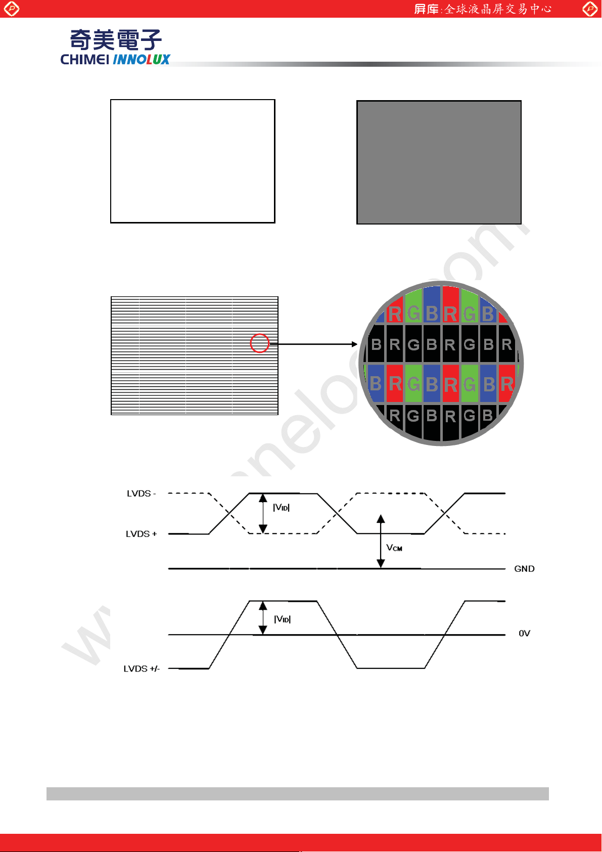
a. White Pattern
Active Area
c. Horizontal Pattern
b. Black Pattern
Active Area
Note (4) The LVDS input characteristics are as follows:
Version 2.1 10 DateΚΚΚΚ6 Jun. 2012
The copyright belongs to CHIMEI InnoLux. Any unauthorized use is prohibited
One step solution for LCD / PDP / OLED panel application: Datasheet, inventory and accessory!
www.panelook.com
Page 11
Global LCD Panel Exchange Center
www.panelook.com
PRODUCT SPECIFICATION
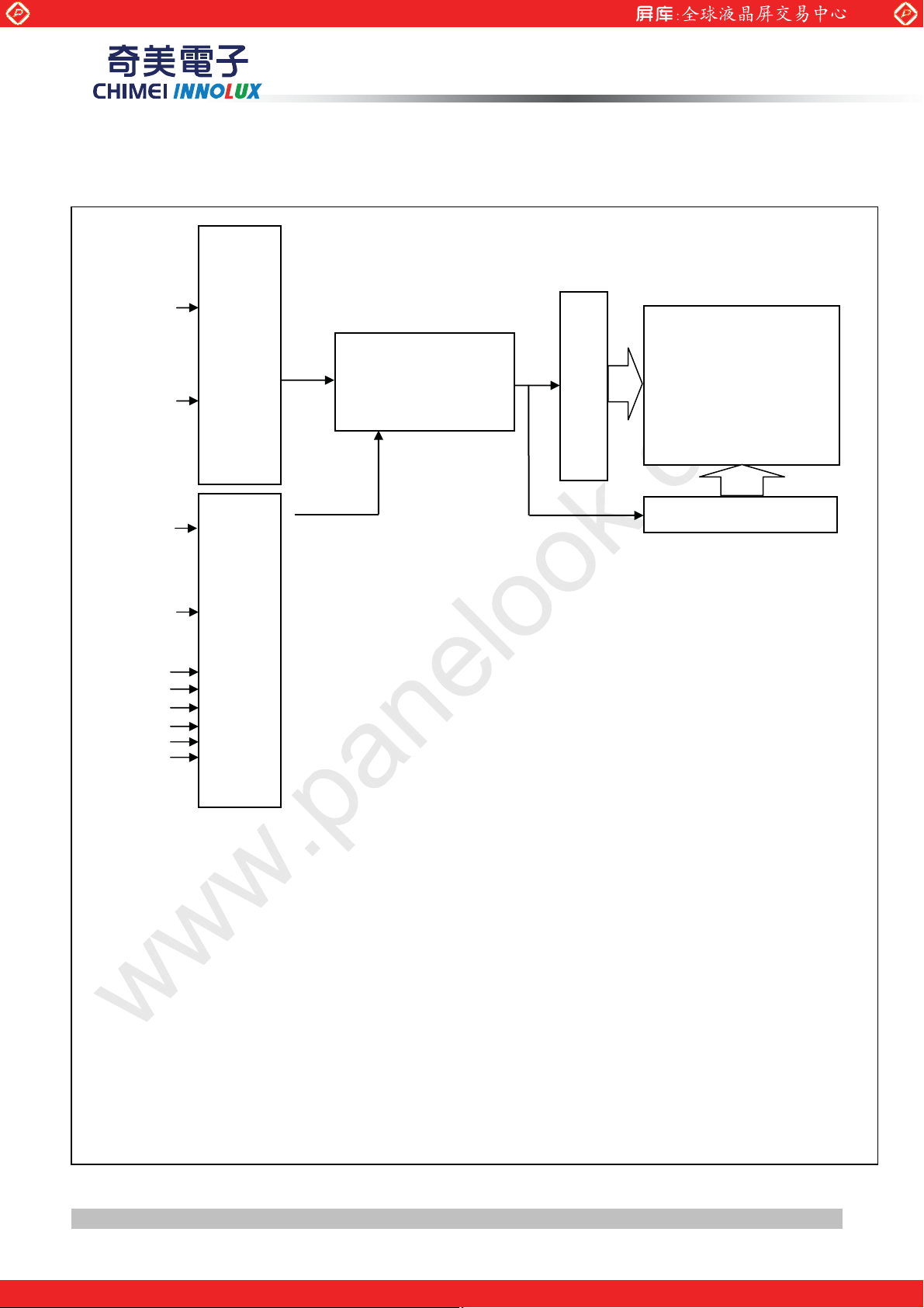
4. BLOCK DIAGRAM OF INTERFACE
4.1 TFT LCD MODULE
INPUT CONNECTOR
CNF2: 187060-41221-P-TWO,
CH3_0(+/-)
CH3_1(+/-)
CH3_2(+/-)
CH3_3(+/-)
CH3_4(+/-)
CH3_CLK(+/-)
CH4_0(+/-)
CH4_1(+/-)
CH4_2(+/-)
CH4_3(+/-)
CH4_4(+/-)
CH4_CLK(+/-)
CH1_0(+/-)
CH1_1(+/-)
CH1_2(+/-)
CH1_3(+/-)
CH1_4(+/-)
CH1_CLK(+/-)
CH2_0(+/-)
CH2_1(+/-)
CH2_2(+/-)
CH2_3(+/-)
CH2_4(+/-)
CH2_CLK(+/-)
SELLVDS
SCN_EN
INPUT CONNECTOR
CNF1: 187059-51221,P-TWO,
CONTROLLER
TIMING
SCAN DRIVER
TFT LCD PANEL
(1920x3x1080)
DATA DRIVER
SDA
VCC
GND
Version 2.1 11 DateΚΚΚΚ6 Jun. 2012
The copyright belongs to CHIMEI InnoLux. Any unauthorized use is prohibited
One step solution for LCD / PDP / OLED panel application: Datasheet, inventory and accessory!
www.panelook.com
Page 12
Global LCD Panel Exchange Center
5 .INPUT TERMINAL PIN ASSIGNMENT
5.1 TFT LCD OPEN CELL
CNF1 Connector Pin Assignment: (FI-RE51S-HF(JAE) or equivalent)
Pin Name Description Note
1 N.C. No Connection (1)
2 SCL EEPROM Serial Clock (for local dimming demo function)
3 SDA EEPROM Serial Data (for local dimming demo function)
www.panelook.com
PRODUCT SPECIFICATION
(5)
4 NC No Connection
5 NC No Connection
6 N.C. No Connection (1)
7 SELLVDS LVDS Data Format Selection (2)(3)
8 N.C. No Connection
9 N.C. No Connection
10 N.C. No Connection
11 GND Ground
12 CH1[0]- First pixel Negative LVDS differential data input. Pair 0
13 CH1[0]+ First pixel Positive LVDS differential data input. Pair 0
14 CH1[1]- First pixel Negative LVDS differential data input. Pair 1
15 CH1[1]+ First pixel Positive LVDS differential data input. Pair 1
16 CH1[2]- First pixel Negative LVDS differential data input. Pair 2
17 CH1[2]+ First pixel Positive LVDS differential data input. Pair 2
1
(1)
ʻˇʼ
18 GND Ground
19 CH1CLK- First pixel Negative LVDS differential clock input.
ʻˇʼ
20 CH1CLK+ First pixel Positive LVDS differential clock input.
21 GND Ground
22 CH1[3]- First pixel Negative LVDS differential data input. Pair 3
23 CH1[3]+ First pixel Positive LVDS differential data input. Pair 3
24 CH1[4]- First pixel Negative LVDS differential data input. Pair 4
25 CH1[4]+ First pixel Positive LVDS differential data input. Pair 4
26 GND Ground
27 NC No Connection
28 CH2[0]- Second pixel Negative LVDS differential data input. Pair 0
Version 2.1 12 DateΚΚΚΚ6 Jun. 2012
The copyright belongs to CHIMEI InnoLux. Any unauthorized use is prohibited
ʻˇʼ
ʻˇʼ
One step solution for LCD / PDP / OLED panel application: Datasheet, inventory and accessory!
www.panelook.com
Page 13
Global LCD Panel Exchange Center
29 CH2[0]+ Second pixel Positive LVDS differential data input. Pair 0
30 CH2[1]- Second pixel Negative LVDS differential data input. Pair 1
www.panelook.com
PRODUCT SPECIFICATION
31 CH2[1]+ Second pixel Positive LVDS differential data input. Pair 1
32 CH2[2]- Second pixel Negative LVDS differential data input. Pair 2
33 CH2[2]+ Second pixel Positive LVDS differential data input. Pair 2
34 GND Ground
35 CH2CLK- Second pixel Negative LVDS differential clock input.
36 CH2CLK+ Second pixel Positive LVDS differential clock input.
37 GND Ground
38 CH2[3]- Second pixel Negative LVDS differential data input. Pair 3
39 CH2[3]+ Second pixel Positive LVDS differential data input. Pair 3
40 CH2[4]- Second pixel Negative LVDS differential data input. Pair 4
41 CH2[4]+ Second pixel Positive LVDS differential data input. Pair 4
42 NC No Connection (5)(3)
43 GND Ground
44 GND Ground
ʻˇʼ
ʻˇʼ
ʻˇʼ
45 GND Ground
46 GND Ground
47 N.C. No Connection (1)
48 VCC +12V power supply
49 VCC +12V power supply
50 VCC +12V power supply
51 VCC +12V power supply
Version 2.1 13 DateΚΚΚΚ6 Jun. 2012
The copyright belongs to CHIMEI InnoLux. Any unauthorized use is prohibited
One step solution for LCD / PDP / OLED panel application: Datasheet, inventory and accessory!
www.panelook.com
Page 14

Global LCD Panel Exchange Center
CNF2 Connector Pin Assignment (FI-RE41S-HF (JAE) or equivalent)
www.panelook.com
PRODUCT SPECIFICATION
Pin Name Description
1 N.C. No Connection
2 N.C. No Connection
3 N.C. No Connection
4 N.C. No Connection
5 N.C. No Connection
6 N.C. No Connection
7 N.C. No Connection
8 N.C. No Connection
9 GND Ground
10 CH3[0]- Third pixel Negative LVDS differential data input. Pair 0
11 CH3[0]+ Third pixel Positive LVDS differential data input. Pair 0
12 CH3[1]- Third pixel Negative LVDS differential data input. Pair 1
13 CH3[1]+ Third pixel Positive LVDS differential data input. Pair 1
ˡ˸ʳ
ʻ˄ʼʳ
ʳ
ʻˇʼʳ
14 CH3[2]- Third pixel Negative LVDS differential data input. Pair 2
15 CH3[2]+ Third pixel Positive LVDS differential data input. Pair 2
16 GND Ground
17 CH3CLK- Third pixel Negative LVDS differential clock input.
18 CH3CLK+ Third pixel Positive LVDS differential clock input.
19 GND Ground
20 CH3[3]- Third pixel Negative LVDS differential data input. Pair 3
21 CH3[3]+ Third pixel Positive LVDS differential data input. Pair 3
22 CH3[4]- Third pixel Negative LVDS differential data input. Pair 4
23 CH3[4]+ Third pixel Positive LVDS differential data input. Pair 4
24 GND Ground
25 GND Ground
26 CH4[0]- Fourth pixel Negative LVDS differential data input. Pair 0
27 CH4[0]+ Fourth pixel Positive LVDS differential data input. Pair 0
ʳ
ʻˇʼʳ
ʳ
ʻˇʼʳ
ʳ
ʳ
28 CH4[1]- Fourth pixel Negative LVDS differential data input. Pair 1
29 CH4[1]+ Fourth pixel Positive LVDS differential data input. Pair 1
30 CH4[2]- Fourth pixel Negative LVDS differential data input. Pair 2
Version 2.1 14 DateΚΚΚΚ6 Jun. 2012
The copyright belongs to CHIMEI InnoLux. Any unauthorized use is prohibited
One step solution for LCD / PDP / OLED panel application: Datasheet, inventory and accessory!
ʻˇʼʳ
www.panelook.com
Page 15

Global LCD Panel Exchange Center
www.panelook.com
PRODUCT SPECIFICATION
31 CH4[2]+ Fourth pixel Positive LVDS differential data input. Pair 2
32 GND Ground
33 CH4CLK- Fourth pixel Negative LVDS differential clock input.
34 CH4CLK+ Fourth pixel Positive LVDS differential clock input.
35 GND Ground
36 CH4[3]- Fourth pixel Negative LVDS differential data input. Pair 3
37 CH4[3]+ Fourth pixel Positive LVDS differential data input. Pair 3
38 CH4[4]- Fourth pixel Negative LVDS differential data input. Pair 4
39 CH4[4]+ Fourth pixel Positive LVDS differential data input. Pair 4
40 GND Ground
41 GND Ground
Note (1) Reserved for internal use. Please leave it open.
Note (2) LVDS format selection.
ʻˇʼʳ
ʳ
ʻˇʼʳ
ʳ
ʻˇʼʳ
L= Connect to GND, H=Connect to +3.3V or open
SELLVDS Note
L JEIDA Format
H or Open VESA Format
Note (3) SELLVDS signal pin connected to the LCM side has the following diagram.
R1 in the system side should be less than 1K Ohm. (R1 < 1K Ohm)
System Board Panel Board
1K ohm
Interface Voltage Level
IC
>20K ohm
VH > 3.0V
VL < 0.7V
Version 2.1 15 DateΚΚΚΚ6 Jun. 2012
The copyright belongs to CHIMEI InnoLux. Any unauthorized use is prohibited
One step solution for LCD / PDP / OLED panel application: Datasheet, inventory and accessory!
www.panelook.com
Page 16

Global LCD Panel Exchange Center
Note (4) LVDS 4-port Data Mapping
Port Channel of LVDS Data Stream
1st Port First Pixel 1, 5, 9, ……1913, 1917
2nd Port Second Pixel 2, 6, 10, ….1914, 1918
3rd Port Third Pixel 3, 7, 11, ….1915, 1919
4th Port Fourth Pixel 4, 8, 12, ….1916, 1920
Note (5) Please reference Appendix A
Note (6) The screw hole which is distant from the connector is merged with Ground
www.panelook.com
PRODUCT SPECIFICATION
Version 2.1 16 DateΚΚΚΚ6 Jun. 2012
The copyright belongs to CHIMEI InnoLux. Any unauthorized use is prohibited
One step solution for LCD / PDP / OLED panel application: Datasheet, inventory and accessory!
www.panelook.com
Page 17

Global LCD Panel Exchange Center
www.panelook.com
PRODUCT SPECIFICATION
AR0~AR9: First pixel R data
Version 2.1 17 DateΚΚΚΚ6 Jun. 2012
The copyright belongs to CHIMEI InnoLux. Any unauthorized use is prohibited
One step solution for LCD / PDP / OLED panel application: Datasheet, inventory and accessory!
www.panelook.com
Page 18

Global LCD Panel Exchange Center
AG0~AG9: First pixel G data
AB0~AB9: First pixel B data
BR0~BR9: Second pixel R data
BG0~BG9: Second pixel G data
BB0~BB9: Second pixel B data
DE: Data enable signal
DCLK: Data clock signal
The third and fourth pixel are followed the same rules.
CR0~CR9: Third pixel R data
CG0~CG9: Third pixel G data
CB0~CB9: Third pixel B data
DR0~DR9: Fourth pixel R data
www.panelook.com
PRODUCT SPECIFICATION
DG0~DG9: Fourth pixel G data
DB0~DB9: Fourth pixel B data
Note (1) A ~ D channel are first, second, third and fourth pixel respectively.
Note (2) The system must have the transmitter to drive the module.
Note (3) LVDS cable impedance shall be 50 ohms per signal line or about 100 ohms per twist-pair line when it is
used differentially.
Version 2.1 18 DateΚΚΚΚ6 Jun. 2012
The copyright belongs to CHIMEI InnoLux. Any unauthorized use is prohibited
One step solution for LCD / PDP / OLED panel application: Datasheet, inventory and accessory!
www.panelook.com
Page 19

Global LCD Panel Exchange Center
5.2 LVDS INTERFACE
JEIDA Format : SELLVDS = L
VESA Format : SELLVDS = H or Open
VESA Format
www.panelook.com
PRODUCT SPECIFICATION
Current Cycle
AR 0P
AR 0N
AR 1P
AR 1N
AR 2P
AR 2N
AR 3P
AR 3N
AR 4P
AR 4N
JEIDA Format
AR 0P
AR 0N
AR 1P
AR 1N
AR0
AG1
AB2
AR6
AR4
AG5
AG0 AR5
AB1
DE VS HS AB5 AB4 AB3 AB2
REV AB7 AB6 AG7 AG6 AR7 AR6
REV AB9 AB8 AG9 AG8 AR9 AR8AR8 REV
AG4 AR7
AB5
AB0 AG5 AG4 AG3 AG2 AG1
AB4 AG7 AG6 AG5AG9 AG8
AR4 AR3 AR2 AR1 AR0
AR6 AR5 AR4AR9 AR8
AG0
AB1
DE
REV
AG4
AB5
AR 2P
AR 2N
AR 3P
AR 3N
AR 4P
AR 4N
AR0~AR9: First Pixel R Data (9; MSB, 0; LSB)
AG0~AG9: First Pixel G Data (9; MSB, 0; LSB)
AB0~AB9: First Pixel B Data (9; MSB, 0; LSB)
DE : Data enable signal
DCLK : Data clock signal
RSV: Reserved
Version 2.1 19 DateΚΚΚΚ6 Jun. 2012
The copyright belongs to CHIMEI InnoLux. Any unauthorized use is prohibited
AB6
AR2
DE VS HS AB7 AB6AB9 AB8
REV AB3 AB2 AG3 AG2 AR3 AR2
REV AB1 AB0 AG1 AG0 AR1 AR0AR0 REV
One step solution for LCD / PDP / OLED panel application: Datasheet, inventory and accessory!
DE
REV
www.panelook.com
Page 20

Global LCD Panel Exchange Center
5.3 COLOR DATA INPUT ASSIGNMENT
The brightness of each primary color (red, green and blue) is based on the 10-bit gray scale data input for the
color. The higher the binary input, the brighter the color. The table below provides the assignment of the color
versus data input.
www.panelook.com
PRODUCT SPECIFICATION
Data Signal
Basic
Colors
Gray
Scale
Of
Red
Color
Black
Red
Green
Blue
Cyan
Magenta
Yellow
White
Red (0) / Dark
Red (1)
Red (2)
:
:
Red (1021)
Red (1022)
Red Green Blue
R9 R8 R7 R6 R5 R4 R3 R2 R1 R0 G9 G8 G7 G6 G5 G4 G3 G2 G1 G0 B9 B8 B7 B6 B5 B4 B3 B2 B1 B0
0
0
0
0
0
0
0
0
0
0
0
0
0
0
0
0
0
0
0
0
0
0
0
0
0
0
0
0
0
0
0
1
1
1
1
1
1
1
1
1
1
0
0
0
0
0
0
0
0
1
1
1
1
1
0
0
0
0
0
0
0
0
0
0
0
0
0
0
0
0
0
0
0
0
0
0
0
1
1
0
0
0
0
0
0
1
1
1
1
1
1
1
1
1
1
1
1
1
1
1
1
1
1
1
1
1
1
1
1
1
1
0
0
0
0
0
0
0
0
0
0
0
0
0
0
0
0
0
0
0
0
0
:
:
:
:
:
:
:
:
:
:
1
1
1
1
1
1
1
1
1
1
1
1
1
1
1
1
1
1
0
0
0
0
1
0
0
1
0
:
:
:
:
:
:
0
1
1
1
1
0
1
0
0
0
1
1
1
1
1
1
0
0
0
0
0
0
0
0
0
:
:
:
:
:
:
0
0
0
0
0
0
1
0
0
0
1
1
1
0
0
0
1
1
1
1
1
1
0
0
0
0
0
0
0
0
0
:
:
:
:
:
:
0
0
0
0
0
0
0
1
1
1
0
0
0
1
1
1
0
0
0
1
1
1
1
1
1
0
0
0
0
0
0
0
0
0
:
:
:
:
:
:
0
0
0
0
0
0
0
0
0
0
0
0
0
0
0
0
0
1
0
0
0
1
1
1
1
0
1
1
0
0
0
:
:
0
0
1
1
1
1
1
1
0
0
0
1
1
1
0
0
0
0
0
0
0
0
0
:
:
:
;
:
:
0
0
0
0
0
0
0
1
1
1
1
1
1
1
1
1
0
0
0
1
1
1
0
0
0
0
0
0
0
0
0
:
:
:
:
:
:
0
0
0
0
0
0
0
0
0
0
0
0
0
1
1
1
1
1
1
1
1
1
0
0
0
1
1
1
0
0
0
0
0
0
0
0
0
:
:
:
:
:
:
0
0
0
0
0
0
0
0
0
1
1
1
0
1
0
0
0
:
:
0
0
0
0
0
0
0
0
0
0
0
0
0
0
0
:
:
:
:
:
:
0
0
0
0
0
0
0
0
0
0
0
0
0
0
0
0
0
1
:
:
:
:
:
:
1
1
0
Gray
Scale
Of
Green
Gray
Scale
Of
Blue
Red (1023)
Green (0) / Dark
Green (1)
Green (2)
:
:
Green (1021)
Green (1022)
Green (1023)
Blue (0) / Dark
Blue (1)
Blue (2)
:
:
Blue (1021)
0
1
1
1
0
0
0
0
0
0
0
0
0
0
1
1
1
1
1
1
1
0
0
0
0
0
0
0
0
0
0
0
0
0
0
0
0
0
0
0
0
0
0
0
0
0
0
0
0
0
0
0
0
0
0
0
0
0
0
0
0
0
0
0
0
0
0
0
0
0
:
:
:
:
:
:
:
:
:
:
:
:
:
:
:
:
:
:
:
:
:
:
:
:
:
:
:
:
:
:
0
0
0
0
0
0
0
0
0
0
1
1
1
1
1
0
0
0
0
0
0
0
0
0
0
1
1
1
1
1
0
0
0
0
0
0
0
0
0
0
1
1
1
1
1
0
0
0
0
0
0
0
0
0
0
0
0
0
0
0
0
0
0
0
0
0
0
0
0
0
0
0
0
0
0
0
0
0
0
0
0
0
0
0
0
0
0
0
0
0
:
:
:
:
:
:
:
:
:
:
:
:
:
:
:
:
:
:
:
:
:
:
:
:
:
:
:
:
:
:
0
0
0
0
0
0
0
0
0
0
0
0
0
0
0
0
0
0
0
0
:
:
:
:
:
:
1
1
1
1
1
1
1
1
1
0
0
0
0
0
0
0
0
0
:
:
:
:
:
:
0
0
0
0
0
0
0
0
1
0
1
0
0
:
:
:
:
:
:
0
1
0
1
0
0
1
1
0
0
0
0
0
0
0
0
0
0
:
:
:
:
:
:
0
0
1
0
0
0
0
0
0
0
0
0
0
:
:
:
:
0
0
0
0
0
0
0
0
0
0
0
0
:
:
:
:
1
1
0
0
0
0
0
0
0
0
:
:
:
:
:
:
0
0
0
0
0
0
0
0
0
0
0
0
0
0
0
0
0
0
:
:
:
:
:
:
1
1
1
Version 2.1 20 DateΚΚΚΚ6 Jun. 2012
The copyright belongs to CHIMEI InnoLux. Any unauthorized use is prohibited
0
0
0
0
:
:
0
0
0
0
1
0
:
:
1
One step solution for LCD / PDP / OLED panel application: Datasheet, inventory and accessory!
www.panelook.com
Page 21

Global LCD Panel Exchange Center
www.panelook.com
PRODUCT SPECIFICATION
Blue (1022)
Blue (1023)
Note (1) 0: Low Level Voltage, 1: High Level Voltage
00000000000000000000000000000000000000001111111111111111110
1
Version 2.1 21 DateΚΚΚΚ6 Jun. 2012
The copyright belongs to CHIMEI InnoLux. Any unauthorized use is prohibited
One step solution for LCD / PDP / OLED panel application: Datasheet, inventory and accessory!
www.panelook.com
Page 22

Global LCD Panel Exchange Center
5.4 FLICKER (Vcom/Gamma) ADJUSTMENT
(1) Adjustment Pattern:
Sub pixel on/off Pattern was shown as below. If customer need below pattern, please directly contact with
Account FAE. (bright sub-pixelΚG128 ; dark sub-pixelΚ G0)
Frame N Frame N+1
www.panelook.com
PRODUCT SPECIFICATION
(2) Adjustment method: (Digital V-com / Gamma)
Programmable memory IC is used for Digital V-com (Gamma) adjustment in this model. CMI provide Auto
V-com (Auto Gamma) tools to adjust Digital V-com (Gamma). The detail connection and setting instruction,
please directly contact with Account FAE or refer CMI Auto V-com (Auto Gamma) adjustment OI. Below
items is suggested to be ready before Digital V-com (Gamma) adjustment in customer LCM line.
Version 2.1 22 DateΚΚΚΚ6 Jun. 2012
The copyright belongs to CHIMEI InnoLux. Any unauthorized use is prohibited
One step solution for LCD / PDP / OLED panel application: Datasheet, inventory and accessory!
www.panelook.com
Page 23

Global LCD Panel Exchange Center
6. INTERFACE TIMING
6.1 INPUT SIGNAL TIMING SPECIFICATIONS
(Ta = 25 ± 2 ºC)
The input signal timing specifications are shown as the following table and timing diagram.
Signal Item Symbol Min. Typ. Max. Unit Note
www.panelook.com
PRODUCT SPECIFICATION
LVDS
Receiver
Clock
LVDS
Receiver
Data
Frequency
Input cycle to
cycle jitter
Spread spectrum
modulation range
Spread spectrum
modulation frequency
Rceiver Skew margin TRSKM -400 400 ps (5)
Fclkin
(=1/TC)
Trcl - - 200 ps (3)
Fclkin_
mod
FSSM - - 200 KHz
73 74.25 75.5 MHz
Fclkin-2% - Fclkin+2% MHz (4)
6.1.1 Timing spec for Frame Rate = 100Hz
Signal Item Symbol Min. Typ. Max. Unit Note
Frame rate 2D mode Fr5 94 100 106 Hz
Ver t ical
Active
Display
2D Mode
Total Tv 1090 1350 1395 Th
Display Tvd 1080 1080 1080 Th
Tv=Tvd+Tv
b
Ё
Term
Horizontal
Active
2D Mode
Display
Term
Version 2.1 23 DateΚΚΚΚ6 Jun. 2012
The copyright belongs to CHIMEI InnoLux. Any unauthorized use is prohibited
Blank Tvb 10 270 315 Th
Total Th 520 550 670 Tc
Display Thd 480 480 480 Tc
Blank Thb 40 70 190 Tc
Display Thd 480 480 480 Tc
Blank Thb 40 70 190 Tc
Ё
Th=Thd+T
hb
Ё
Ё
Ё
Ё
One step solution for LCD / PDP / OLED panel application: Datasheet, inventory and accessory!
www.panelook.com
Page 24

Global LCD Panel Exchange Center
6.1.2 Timing spec for Frame Rate = 120Hz
Signal Item Symbol Min. Typ. Max. Unit Note
Frame rate 2D mode Fr6 114 120 126 Hz
www.panelook.com
PRODUCT SPECIFICATION
Ver t ical
Active
Display
Term
2D Mode
Total Tv 1090 1125 1395 Th
Display Tvd 1080 1080 1080 Th
Blank Tvb 10 45 315 Th
Tv=Tvd+Tv
b
Ё
Ё
Th=Thd+T
Horizontal
Active
2D Mode
Total Th 520 550 670 Tc
hb
Display Thd 480 480 480 Tc
Ё
Display
Blank Thb 40 70 190 Tc
Ё
Term
Blank Thb 40 70 190 Tc
Ё
(Note (1) Since the module is operated in DE only mode, Hsync and Vsync input signals should be set to low
logic level. Otherwise, this module would operate abnormally.
Note (2ʼʳ ʳ ˣ˿˸˴˸ʳ˴˾˸ʳ˸ʳ˻˸ʳ˴˺˸ʳ˹ʳ˼˸˿ʳ˶˿˶˾ʳ˻˴ʳ˹˿˿ʳ˻˸ʳ˵˸˿ʳ˸˴˼ˍʳ ʳ ʳ
˙
˶˿˾˼ʻ˴ʼ
˙
ˈ
ʳЊʳ˙
ˉ
ʳѼʳ˧ʳѼʳ˧˻
ʳѼʳ˧ʳѼʳ˧˻ʳЊʳ˙
˶˿˾˼ʻ˼ʼ
ʳ
ʳ
Version 2.1 24 DateΚΚΚΚ6 Jun. 2012
The copyright belongs to CHIMEI InnoLux. Any unauthorized use is prohibited
One step solution for LCD / PDP / OLED panel application: Datasheet, inventory and accessory!
www.panelook.com
Page 25

Global LCD Panel Exchange Center
DE
T
h
www.panelook.com
WZKhd ^W/&/d/KE
INPUT SIGNAL TIMING DIAGRAM
T
v
T
vd
T
vb
DCLK
T
c
T
hb
T
hd
DE
DATA
Valid display data ( 960 clocks)
Note (3) The input clock cycle-to-cycle jitter is defined as below figures. Trcl = I T1 – TI
Version 2.1 25 DateΚΚΚΚ6 Jun. 2012
The copyright belongs to CHIMEI InnoLux. Any unauthorized use is prohibited
One step solution for LCD / PDP / OLED panel application: Datasheet, inventory and accessory!
www.panelook.com
Page 26

Global LCD Panel Exchange Center
www.panelook.com
WZKhd ^W/&/d/KE
Note (4) The SSCG (Spread spectrum clock generator) is defined as below figures.
Note (5) LVDS receiver skew margin is defined and shown as below.
LVDS RECEIVER INTERFACE TIMING DIAGRAM
Tc
RXCLK+/-
RXn+/-
T
RSKM
Version 2.1 26 DateΚΚΚΚ6 Jun. 2012
The copyright belongs to CHIMEI InnoLux. Any unauthorized use is prohibited
One step solution for LCD / PDP / OLED panel application: Datasheet, inventory and accessory!
www.panelook.com
Page 27

Global LCD Panel Exchange Center
P
6.2 POWER ON/OFF SEQUENCE
(Ta = 25 ± 2 ºC)
To prevent a latch-up or DC operation of LCD module, the power on/off sequence should be as the diagram
below.
0V
0.5ЉЉЉЉT1ЉЉЉЉ10ms
0ЉЉЉЉT
0ЉЉЉЉT
500ms ЉЉЉЉT
LVDS Signals
2
ЉЉЉЉ50ms
3
ЉЉЉЉ50ms
4
0V
www.panelook.com
0.1V
CC
Power On
WZKhd ^W/&/d/KE
0.1V
cc
T
T
1
T
2
VALID
3
T
4
0ЉЉЉЉT7ЉЉЉЉT2
8
0ЉЉЉЉT
ЉЉЉЉT3
T
T
7
8
Option Signals
(SELLVDS,…)
Backlight (Recommended)
500msЉЉЉЉT
100ms
ЉЉЉЉ
5
T
6
50%
T
5
50%
6
T
Power ON/OFF Sequence
Note (1) The supply voltage of the external system for the module input should follow the definition of Vcc.
Note (2) Apply the lamp voltage within the LCD operation range. When the backlight turns on before the LCD
operation or the LCD turns off before the backlight turns off, the display may momentarily become
abnormal screen.
Note (3) In case of Vcc is in off level, please keep the level of input signals on the low or high impedance. If
T2<0,that maybe cause electrical overstress failure.
Note (4) T4 should be measured after the module has been fully discharged between power off and on period.
Note (5) Interface signal shall not be kept at high impedance when the power is on.
Version 2.1 27 DateΚΚΚΚ6 Jun. 2012
The copyright belongs to CHIMEI InnoLux. Any unauthorized use is prohibited
One step solution for LCD / PDP / OLED panel application: Datasheet, inventory and accessory!
www.panelook.com
Page 28

Global LCD Panel Exchange Center
7. OPTICAL CHARACTERISTICS
7.1 TEST CONDITIONS
Item Symbol Value Unit
Ambient Temperature Ta
Ambient Humidity Ha
Supply Voltage VCC 12V V
Input Signal According to typical value in "3. ELECTRICAL CHARACTERISTICS"
LED Current IL 160 mA
The LCD module should be stabilized at given temperature for 1 hour to avoid abrupt temperature change during
measuring in a windless room.
www.panelook.com
WZKhd ^W/&/d/KE
25±2
50±10
o
C
%RH
Version 2.1 28 DateΚΚΚΚ6 Jun. 2012
The copyright belongs to CHIMEI InnoLux. Any unauthorized use is prohibited
One step solution for LCD / PDP / OLED panel application: Datasheet, inventory and accessory!
www.panelook.com
Page 29

Global LCD Panel Exchange Center
7.2 OPTICAL SPECIFICATIONS
The relative measurement methods of optical characteristics are shown as below. The following items should
be measured under the test conditions described in 7.1 and stable environment shown in 7.1.
Item Symbol Condition Min. Typ. Max. Unit Note
www.panelook.com
WZKhd ^W/&/d/KE
Rcx
0.659
-
Red
Color
Chromaticity
Green
Blue
Rcy
Gcx
Gcy
Bcx
Bcy
Wcx
θ
=0°, θY =0°
x
Viewing Angle at Normal
Direction
Standard light source “C”
0.324
0.267
0.585
-
-
0.133
0.107
0.304
-
-
-
-
(0)
-
-
White
Wcy
Center Transmittance T% - 6.4 - % (1),(6)
Contrast Ratio CR
Gray to
Response Time
gray
White Variation
δW
θ
=0°, θY =0°
x
with CMI module
θ
=0°, θY =0°
x
with CMI Module
θ
=0°, θY =0°
x
4200 6000
- 6 12 ms (1),(4)
- - 1.3 - (1),(5)
0.361
- - (1),(3)
-
with CMI module
θx+
-
88
-
Horizontal
Viewing
θ
-
x
CR≥20
-
88
Deg. (1),(2)
Angle
θY+
With CMI module
-
88
-
Ver t ical
θ
-
Y
-
88
-
Note (0) Light source is the standard light source ”C” which is defined by CIE and driving voltage are based on
suitable gamma voltages. The calculating method is as following:
1. Measure Module’s and BLU’s spectrum at center point. White and R,G,B are with signal input. BLU (for
V546HK3-LS5) is supplied by CMI.
2. Calculate cell’s spectrum.
3. Calculate cell’s chromaticity by using the spectrum of standard light source “C”.
Note (1) Light source is the BLU which supplied by CMI and driving voltage are based on suitable gamma voltages.
Version 2.1 29 DateΚΚΚΚ6 Jun. 2012
The copyright belongs to CHIMEI InnoLux. Any unauthorized use is prohibited
One step solution for LCD / PDP / OLED panel application: Datasheet, inventory and accessory!
www.panelook.com
Page 30

Global LCD Panel Exchange Center
Note (2) Definition of Viewing Angle (θx, θy):
Viewing angles are measured by Autronic Conoscope Cono-80
www.panelook.com
WZKhd ^W/&/d/KE
Normal
θx = θy = 0º
θy- θy+
θX- = 90º
6 o’clock
θ
y-
= 90º
x-
y-
Note (3) Definition of Contrast Ratio (CR):
The contrast ratio can be calculated by the following expression.
Contrast Ratio (CR) =
L255: Luminance of gray level 255
L 0: Luminance of gray level 0
CR = CR (5), where CR (X) is corresponding to the Contrast Ratio of the point X at the figure in Note (5).
θx−
θx+
L0 of LuminanceSurface
12 o’clock direction
y+
θ
y+
= 90º
x+
θX+ = 90º
L255of LuminanceSurface
Note (4) Definition of Gray-to-Gray Switching Time:
100%
90%
Optical
Response
10%
0%
Gray to gray
switching time
Gray to gray
switching time
Time
The driving signal means the signal of gray level 0, 124, 252, 380, 508, 636, 764, 892 and 1023.
Gray to gray average time means the average switching time of gray level 0, 124, 252, 380, 508, 636,
764, 892 and 1023 to each other.
Note (5) Definition of White Variation (δW):
Version 2.1 30 DateΚΚΚΚ6 Jun. 2012
The copyright belongs to CHIMEI InnoLux. Any unauthorized use is prohibited
One step solution for LCD / PDP / OLED panel application: Datasheet, inventory and accessory!
www.panelook.com
Page 31

Global LCD Panel Exchange Center
Measure the luminance of gray level 255 at 5 points
δW = Maximum [L (1), L (2), L (3), L (4), L (5)] / Minimum [L (1), L (2), L (3), L (4), L (5)]
www.panelook.com
WZKhd ^W/&/d/KE
Horizontal Line
D
D/4 D/2 3D/4
1 2
W
W/4
W/2
Vertical Line
3W/4
3 4
Note (6) Definition of Transmittance (T%) :
Measure the luminance of gray level 255 at center point of LCD module.
Transmittance (T%) =
5
Active Area
X
: Test Point
X=1 to 5
moduleLCDof Luminance
100%
unitbacklighof Luminance
×
Version 2.1 31 DateΚΚΚΚ6 Jun. 2012
The copyright belongs to CHIMEI InnoLux. Any unauthorized use is prohibited
One step solution for LCD / PDP / OLED panel application: Datasheet, inventory and accessory!
www.panelook.com
Page 32

Global LCD Panel Exchange Center
www.panelook.com
WZKhd ^W/&/d/KE
8.PRECAUTIONS
8.1 ASSEMBLY AND HANDLING PRECAUTIONS
[ 1 ] Do not apply rough force such as bending or twisting to the module during assembly.
[ 2 ] It is recommended to assemble or to install a module into the user’s system in clean working areas. The dust
and oil may cause electrical short or worsen the polarizer.
[ 3 ] Do not apply pressure or impulse to the module to prevent the damage of LCD panel and Backlight.
[ 4 ] Always follow the correct power-on sequence when the LCD module is turned on. This can prevent the
damage and latch-up of the CMOS LSI chips.
[ 5 ] Do not plug in or pull out the I/F connector while the module is in operation.
[ 6 ] Do not disassemble the module.
[ 7 ] Use a soft dry cloth without chemicals for cleaning, because the surface of polarizer is very soft and easily
scratched.
[ 8 ] Moisture can easily penetrate into LCD module and may cause the damage during operation.
[ 9 ] When storing modules as spares for a long time, the following precaution is necessary.
[ 9.1 ] Do not leave the module in high temperature, and high humidity for a long time. It is highly
recommended to store the module with temperature from 0 to 35кat normal humidity without
condensation.
[ 9.2 ] The module shall be stored in dark place. Do not store the TFT-LCD module in direct sunlight or
fluorescent light.
[ 10 ] When ambient temperature is lower than 10ºC, the display quality might be reduced. For example, the
response time will become slow, and the starting voltage of CCFL will be higher than that of room
temperature.
8.2 SAFETY PRECAUTIONS
[ 1 ] The startup voltage of a Backlight is approximately 1000 Volts. It may cause an electrical shock while
assembling with the inverter. Do not disassemble the module or insert anything into the Backlight unit.
[ 2 ] If the liquid crystal material leaks from the panel, it should be kept away from the eyes or mouth. In case of
contact with hands, skin or clothes, it has to be washed away thoroughly with soap.
[ 3 ] After the module’s end of life, it is not harmful in case of normal operation and storage.
Version 2.1 32 DateΚΚΚΚ6 Jun. 2012
The copyright belongs to CHIMEI InnoLux. Any unauthorized use is prohibited
One step solution for LCD / PDP / OLED panel application: Datasheet, inventory and accessory!
www.panelook.com
Page 33

Global LCD Panel Exchange Center
9. DEFINITION OF LABELS
9.1 OPEN CELL LABEL
The barcode nameplate is pasted on each open cell as illustration for CMI internal contro
Model Name: V546HK3-PS1
Revision: Rev. XX, for example: A0, A1… B1, B2… or C1, C2…etc.
Serial ID: X X X X X X X Y M D L N N N N
www.panelook.com
WZKhd ^W/&/d/KE
V546HK3 –PS1 Rev. XX
X X X X X X X Y M D L N N N N
Figure.8-1 Serial No. Label on SPWB
Serial No.
Year, Month, Date
CMI Internal Use
Revision
Serial ID includes the information as below:
Manufactured Date:
Year: 2010=0, 2011=1,2012=2…etc.
Month: 1~9, A~C, for Jan. ~ Dec.
Day: 1~9, A~Y, for 1st to 31st, exclude I ,O, and U.
Revision Code: Cover all the change
Serial No.: Manufacturing sequence of product
CMI Internal Use
Version 2.1 33 DateΚΚΚΚ6 Jun. 2012
The copyright belongs to CHIMEI InnoLux. Any unauthorized use is prohibited
One step solution for LCD / PDP / OLED panel application: Datasheet, inventory and accessory!
www.panelook.com
Page 34

Global LCD Panel Exchange Center
Figure.9-2 Panel ID Label on Cell
Panel ID Label includes the information as below:
Panel ID: T X X X X X X X X X X X
www.panelook.com
WZKhd ^W/&/d/KE
TXXXXXXXXXXX
CMI Internal Use
FAB Line: 1~8, for Fab1~Fab8
TFT
Version 2.1 34 DateΚΚΚΚ6 Jun. 2012
The copyright belongs to CHIMEI InnoLux. Any unauthorized use is prohibited
One step solution for LCD / PDP / OLED panel application: Datasheet, inventory and accessory!
www.panelook.com
Page 35

Global LCD Panel Exchange Center
9.2 CARTON LABEL
The barcode nameplate is pasted on each box as illustration, and its definitions are as following explanation.
www.panelook.com
WZKhd ^W/&/d/KE
!
!
!
(a) Model Name: V546HK3– PS1
(b) Carton ID: X X X X X X X Y M D X X X X
CMI Internal Use
Year, Month, Date
CMI Internal Use
Revision
CMI Internal Use
Serial ID includes the information as below:
Manufactured Date:
Year: 2010=0, 2011=1,2012=2…etc.
Month: 1~9, A~C, for Jan. ~ Dec.
Day: 1~9, A~Y, for 1st to 31st, exclude I ,O, and U.
Revision Code: Cover all the change
(c) Quantities: 8
Version 2.1 35 DateΚΚΚΚ6 Jun. 2012
The copyright belongs to CHIMEI InnoLux. Any unauthorized use is prohibited
One step solution for LCD / PDP / OLED panel application: Datasheet, inventory and accessory!
www.panelook.com
Page 36

Global LCD Panel Exchange Center
10. Packaging
10.1 PACKING SPECIFICATIONS
(1) 8 LCD TV Panels / 1 Box
(2) Box dimensions : 1320 (L) X910 (W) X99 (H)mm
(3) Weight : approximately 40 Kg ( 8 panels per box)
(4) 88 LCD TV Panels / 1 Group
10.2 PACKING METHOD
Figures 10-1 and 10-2 are the packing method
www.panelook.com
WZKhd ^W/&/d/KE
Figure.10-1 packing method
Version 2.1 36 DateΚΚΚΚ6 Jun. 2012
The copyright belongs to CHIMEI InnoLux. Any unauthorized use is prohibited
One step solution for LCD / PDP / OLED panel application: Datasheet, inventory and accessory!
www.panelook.com
Page 37

Global LCD Panel Exchange Center
www.panelook.com
WZKhd ^W/&/d/KE
Figure. 10-2 Packing method
Version 2.1 37 DateΚΚΚΚ6 Jun. 2012
The copyright belongs to CHIMEI InnoLux. Any unauthorized use is prohibited
One step solution for LCD / PDP / OLED panel application: Datasheet, inventory and accessory!
www.panelook.com
Page 38

Global LCD Panel Exchange Center
11. MECHANICAL CHARACTERISTIC
!
!
!
!
!
!
!
!
!
!
!
!
www.panelook.com
WZKhd ^W/&/d/KE
!
!
!
!
!
!
!
!
!
!
!
!
!
!
!
!
!
!
!
!
!
!
!
!
!
Version 2.1 38 DateΚΚΚΚ6 Jun. 2012
The copyright belongs to CHIMEI InnoLux. Any unauthorized use is prohibited
One step solution for LCD / PDP / OLED panel application: Datasheet, inventory and accessory!
www.panelook.com
Page 39

Global LCD Panel Exchange Center
!
!
www.panelook.com
WZKhd ^W/&/d/KE
Version 2.1 39 DateΚΚΚΚ6 Jun. 2012
The copyright belongs to CHIMEI InnoLux. Any unauthorized use is prohibited
One step solution for LCD / PDP / OLED panel application: Datasheet, inventory and accessory!
www.panelook.com
Page 40

Global LCD Panel Exchange Center
www.panelook.com
WZKhd ^W/&/d/KE
Appendix A
Local Dimming demo function
A.1 I2C address and write command
Device address: 0xC2
Register address: 0x01
Command data: 0x00: Local Dimming demo mode OFF (Note 1)
0x01: Local Dimming demo mode ON (Demo in right half screen) (Note 2)
Device Address Register Address
START
11000010
ACK
(0xC2)
Note 1: Local Dimming demo OFF
00000001
(0x01)
ACK
Command Data
00000001
(0x01)
ACK
STOP
Note 2: Local Dimming demo ON
A.2 I2C timing
Version 2.1 40 DateΚΚΚΚ6 Jun. 2012
The copyright belongs to CHIMEI InnoLux. Any unauthorized use is prohibited
One step solution for LCD / PDP / OLED panel application: Datasheet, inventory and accessory!
www.panelook.com
Page 41

Global LCD Panel Exchange Center
Symbol Parameter Min. Max. Unit
www.panelook.com
WZKhd ^W/&/d/KE
t
SU-STA
t
HD-STA
t
SU-DAT
t
HD-DAT
t
SU-STO
t
BUF
Start setup time 250 - ns
Start hold time 250 - ns
Data setup time 80 - ns
Data hold time 0 - ns
Stop setup time 250 - ns
Time between Stop condition and
500 - ns
next Start condition
Version 2.1 41 DateΚΚΚΚ6 Jun. 2012
The copyright belongs to CHIMEI InnoLux. Any unauthorized use is prohibited
One step solution for LCD / PDP / OLED panel application: Datasheet, inventory and accessory!
www.panelook.com
 Loading...