

Page 1
Global LCD Panel Exchange Center
MODEL NO.: V500HK1
www.panelook.com
PRODUCT SPECIFICATION
ϭ Tentative Specification
ϭ Preliminary Specification
Ϯ Approval Specification
SUFFIX: PS5
Customer:
CONFIRMED BY SIGNATURE
Name / Title
APPROVED BY SIGNATURE
Name / Title
Note
Approved By Checked By Prepared By
Chao-Chun Chung Ken Wu WT Hsu
Version 2.0 1 DateΚΚΚΚ8 Mar . 2012
The copyright belongs to CHIMEI InnoLux. Any unauthorized use is prohibited
One step solution for LCD / PDP / OLED panel application: Datasheet, inventory and accessory!
www.panelook.com
Page 2
Global LCD Panel Exchange Center
www.panelook.com
PRODUCT SPECIFICATION
CONTENTS
REVISION HISTORY.........................................................................................................................................................4
1. GENERAL DESCRIPTION............................................................................................................................................ 5
1.1 OVERVIEW ......................................................................................................................................................5
1.2 FEATURES.......................................................................................................................................................5
2. ABSOLUTE MAXIMUM RATINGS ................................................................................................................................6
2.1 ABSOLUTE RATINGS OF ENVIRONMENT ....................................................................................................6
2.2 PACKAGE STORAGE......................................................................................................................................7
2.3 ELECTRICAL ABSOLUTE RATINGS ..............................................................................................................7
3. ELECTRICAL CHARACTERISTICS ............................................................................................................................. 8
3.1 TFT LCD MODULE ..........................................................................................................................................8
4. BLOCK DIAGRAM OF INTERFACE ........................................................................................................................... 11
4.1 TFT LCD MODULE ........................................................................................................................................ 11
5. INPUT TERMINAL PIN ASSIGNMENT.......................................................................................................................12
5.1 TFT LCD OPEN CELL ...................................................................................................................................12
5.2 LVDS INTERFACE.........................................................................................................................................20
5.3 COLOR DATA INPUT ASSIGNMENT ............................................................................................................21
5.4 FLICKER (Vcom) ADJUSTMENT .................................................................................................................. 22
6. INTERFACE TIMING...................................................................................................................................................23
6.1 INPUT SIGNAL TIMING SPECIFICATIONS (Ta = 25 ± 2 ºC)........................................................................23
6.1.1 Timing spec for Frame Rate = 50Hz ...........................................................................................................23
6.1.2 Timing spec for Frame Rate = 60Hz ...........................................................................................................24
6.2 POWER ON/OFF SEQUENCE (Ta = 25 ± 2 ºC) ........................................................................................... 28
6.2.1
POWER ON/OFF SEQUENCE
6.2.2
2D/3D MODE CHANGE SIGNAL SEQUENCE WITHOUT VCC TURN OFF AND TURN ON
7. PRECAUTIONS...........................................................................................................................................................31
7.1 ASSEMBLY AND HANDLING PRECAUTIONS .............................................................................................31
8. DEFINITION OF LABELS............................................................................................................................................32
9. PACKAGING Κ..........................................................................................................................................................33
..............................................................................................................28
Version 2.0 2 DateΚΚΚΚ8 Mar . 2012
The copyright belongs to CHIMEI InnoLux. Any unauthorized use is prohibited
One step solution for LCD / PDP / OLED panel application: Datasheet, inventory and accessory!
....29
www.panelook.com
Page 3

Global LCD Panel Exchange Center
www.panelook.com
PRODUCT SPECIFICATION
9.1 PACKAGING SPECIFICATIONS ...................................................................................................................33
9.2 PACKAGING METHOD..................................................................................................................................33
10. MECHANICAL DRAWING.........................................................................................................................................36
Appendix A.......................................................................................................................................................................37
Version 2.0 3 DateΚΚΚΚ8 Mar . 2012
The copyright belongs to CHIMEI InnoLux. Any unauthorized use is prohibited
One step solution for LCD / PDP / OLED panel application: Datasheet, inventory and accessory!
www.panelook.com
Page 4

Global LCD Panel Exchange Center
Version Date Page(New) Section Description
Ver. 2.0 8,Mar 2012
19,Jun 2012
All
36
www.panelook.com
PRODUCT SPECIFICATION
REVISION HISTORY
All
10
The Approval specification was first issued.
Update MECHANICAL DRAWING
Version 2.0 4 DateΚΚΚΚ8 Mar . 2012
The copyright belongs to CHIMEI InnoLux. Any unauthorized use is prohibited
One step solution for LCD / PDP / OLED panel application: Datasheet, inventory and accessory!
www.panelook.com
Page 5

Global LCD Panel Exchange Center
1. GENERAL DESCRIPTION
1.1 OVERVIEW
35-D076901 is a control board for V500HK1-PS5 model.
1.2 FEATURES
CHARACTERISTICS ITEMS SPECIFICATIONS
Interface 2ch LVDS.
White tracking function Support white tracking function.
Over drive Support over drive function.
Color Depth 8 bit
www.panelook.com
PRODUCT SPECIFICATION
Version 2.0 5 DateΚΚΚΚ8 Mar . 2012
The copyright belongs to CHIMEI InnoLux. Any unauthorized use is prohibited
One step solution for LCD / PDP / OLED panel application: Datasheet, inventory and accessory!
www.panelook.com
Page 6
Global LCD Panel Exchange Center
2. ABSOLUTE MAXIMUM RATINGS
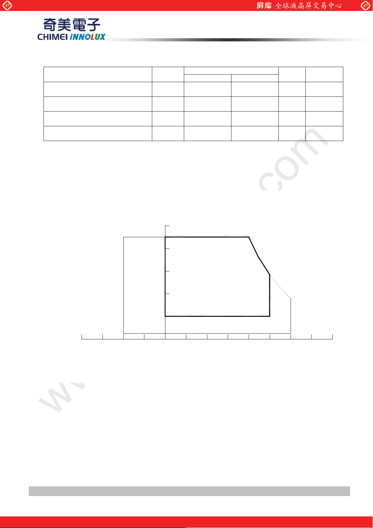
2.1 ABSOLUTE RATINGS OF ENVIRONMENT
Item
www.panelook.com
PRODUCT SPECIFICATION
ymbol
Value
Min. Max.
Unit Note
Storage Temperature
Operating Ambient Temperature
Altitude Operating
Altitude Storage
Note (1) Temperature and relative humidity range is shown in the figure below.
(a) 90 %RH Max. (Ta Љ 40 ºC).
(b) Wet-bulb temperature should be 39 ºC Max. (Ta > 40 ºC).
(c) No condensation..
ST
OP
OP
ST
-20 +60 C (1), (3)
0 50 C (1), (2), (3)
0 5000 (3)
0 12000 (3)
Relative Humidity (%RH)
100
90
80
60
Operating Range
40
20
10
Storage Range
8060-20 400 20-40
Temperature (ºC)
Note (2) The maximum operating temperature is based on the test condition that the surface temperature
of display area is less than or equal to 65 ºC with LCD module alone in a temperature controlled
chamber. Thermal management should be considered in your product design to prevent the
surface temperature of display area from being over 65 ºC. The range of operating temperature
may degrade in case of improper thermal management in your product design.
Note (3) The rating of environment is base on LCD module. Leave LCD cell alone, this environment
condition can’t be guaranteed. Except LCD cell, the customer has to consider the ability of other
parts of LCD module and LCD module process.
Version 2.0 6 DateΚΚΚΚ8 Mar . 2012
The copyright belongs to CHIMEI InnoLux. Any unauthorized use is prohibited
One step solution for LCD / PDP / OLED panel application: Datasheet, inventory and accessory!
www.panelook.com
Page 7
Global LCD Panel Exchange Center
2.2 PACKAGE STORAGE
Storage condition: With shipping package.
Storage temperature rang: 255к
Storage humidity range: 5010%RH
Shelf life: a month
2.3 ELECTRICAL ABSOLUTE RATINGS
Item Symbol
Power Supply Voltage VCC -0.3 13.5 V
Logic Input Voltage VIN -0.3 3.6 V
www.panelook.com
PRODUCT SPECIFICATION
Value
Unit Note
Min. Max.
(1)
Note (1) Permanent damage to the device may occur if maximum values are exceeded. Function
operation should be restricted to the conditions described under Normal Operating Conditions.
Version 2.0 7 DateΚΚΚΚ8 Mar . 2012
The copyright belongs to CHIMEI InnoLux. Any unauthorized use is prohibited
One step solution for LCD / PDP / OLED panel application: Datasheet, inventory and accessory!
www.panelook.com
Page 8
Global LCD Panel Exchange Center
3. ELECTRICAL CHARACTERISTICS
3.1 TFT LCD MODULE
( Ta = 25 ± 2 ºC )
Parameter Symbol
Power Supply Voltage VCC 10.8 12 13.2 V (1)
www.panelook.com
PRODUCT SPECIFICATION
Value
Unit Note
Min. Typ. Max.
Rush Current I
White Pattern
Power Consumption
Horizontal Stripe
Black Pattern
White Pattern
Power Supply Current
Horizontal Stripe
Black Pattern
Differential Input High
Threshold Voltage
Differential Input Low
Threshold Voltage
LVDS
interface
Common Input Voltage VCM 1.0 1.2 1.4 V
Differential input voltage
(single-end)
Terminating Resistor R
CMIS
interface
Input High Threshold Voltage VIH 2.7
Input Low Threshold Voltage V
RUSH
ЁЁ
ЁЁ
ЁЁ
ЁЁ
ЁЁ
ЁЁ
ЁЁ
V
V
LVT H
|V
LVT L
ID
T
IL
+100
ЁЁ
| 200
Ё
0
3.06 A (2)
6.6 7.1 W
14 18.1 W
6.5 7.0 W
0.55 0.60 A
1.2 1.5 A
0.54 0.59 A
ЁЁ
mV
-100 mV
Ё
100
Ё
Ё
600 mV
Ё
ohm
3.3 V
0.7 V
(3)
(4)
Note (1) The module should be always operated within the above ranges.
Note (2) Measurement condition:
Version 2.0 8 DateΚΚΚΚ8 Mar . 2012
The copyright belongs to CHIMEI InnoLux. Any unauthorized use is prohibited
One step solution for LCD / PDP / OLED panel application: Datasheet, inventory and accessory!
www.panelook.com
Page 9
Global LCD Panel Exchange Center
www.panelook.com
PRODUCT SPECIFICATION
(Low to High)
Control Signal
SW
+12 V
Vcc
Q1 Si4485DY
Fuse
R1
1k
VR1
47k
R2
1k
Q2
2N7002
C1
0.01uF
(LCD Module Input)
C3
1uF
Vcc rising time is 470us
Vcc
GND
0.9Vcc
0.1Vcc
470us
Version 2.0 9 DateΚΚΚΚ8 Mar . 2012
The copyright belongs to CHIMEI InnoLux. Any unauthorized use is prohibited
One step solution for LCD / PDP / OLED panel application: Datasheet, inventory and accessory!
www.panelook.com
Page 10
Global LCD Panel Exchange Center
Note (3) The specified power supply current is under the conditions at Vcc = 12 V, Ta = 25 ± 2 ºC, fv = 60 Hz,
whereas a power dissipation check pattern below is displayed.
www.panelook.com
PRODUCT SPECIFICATION
a. White Pattern
Active Area
c. Horizontal Pattern
b. Black Pattern
Active Area
Note (4) The LVDS input characteristics are as follows :
Version 2.0 10 DateΚΚΚΚ8 Mar . 2012
The copyright belongs to CHIMEI InnoLux. Any unauthorized use is prohibited
One step solution for LCD / PDP / OLED panel application: Datasheet, inventory and accessory!
www.panelook.com
Page 11
Global LCD Panel Exchange Center
4. BLOCK DIAGRAM OF INTERFACE
4.1 TFT LCD MODULE
www.panelook.com
PRODUCT SPECIFICATION
CH1_0(+/-)
CH1_1(+/-)
CH1_2(+/-)
CH1_3(+/-)
CH1_CLK(+/-)
CH2_0(+/-)
CH2_1(+/-)
CH2_2(+/-)
CH2_3(+/-)
CH2_CLK(+/-)
SELLVDS
2D/3D
L/R
LD_EN
SCN EN
GND
L/R_O
SCL
SDA
INPUT CONNECTOR
WF23-400-513C-FCN,
TIMING
CONTROLLER
DC/DC CONVERTER
& REFERENCE
VOLTAGE
SCAN DRIVER
TFT LCD PANEL
(1920x3x1080)
DATA DRIVER
L/R_O
CN6:LM123S-010-H-TF1-3
or equivalent
Version 2.0 11 DateΚΚΚΚ8 Mar . 2012
The copyright belongs to CHIMEI InnoLux. Any unauthorized use is prohibited
OUTPUT CONNECTOR
One step solution for LCD / PDP / OLED panel application: Datasheet, inventory and accessory!
www.panelook.com
Page 12
Global LCD Panel Exchange Center
5. INPUT TERMINAL PIN ASSIGNMENT
5.1 TFT LCD OPEN CELL
CNF1 Connector Pin Assignment: (WF23-400-513C-FCN or equivalent)
Pin Name Description Note
1 N.C. No Connection (1)
2 SCL I2C Serial Clock (for 3D format selection function)
3 SDA I2C Serial Data (for 3D format selection function)
4 AGMODE Aging Mode (12)
5 L/R_O Output signal for Left Right Glasses control (10)
6 N.C. No Connection (1)
7 SELLVDS Input signal for LVDS Data Format Selection (2)(7)
www.panelook.com
PRODUCT SPECIFICATION
(11)
8 N.C. No Connection
9 N.C. No Connection
10 N.C. No Connection
11 GND Ground
12 ORX0- Odd pixel Negative LVDS differential data input. Channel 0
13 ORX0+ Odd pixel Positive LVDS differential data input. Channel 0
14 ORX1- Odd pixel Negative LVDS differential data input. Channel 1
15 ORX1+ Odd pixel Positive LVDS differential data input. Channel 1
16 ORX2- Odd pixel Negative LVDS differential data input. Channel 2
17 ORX2+ Odd pixel Positive LVDS differential data input. Channel 2
18 GND Ground
19 OCLK- Odd pixel Negative LVDS differential clock input
20 OCLK+ Odd pixel Positive LVDS differential clock input
21 GND Ground
(1)
(9)
(9)
22 ORX3- Odd pixel Negative LVDS differential data input. Channel 3
23 ORX3+ Odd pixel Positive LVDS differential data input. Channel 3
24 N.C. No Connection
25 N.C. No Connection
26 2D/3D Input signal for 2D/3D Mode Selection (3)(6)(8)
27 L/R
28 ERX0- Even pixel Negative LVDS differential data input. Channel 0
29 ERX0+ Even pixel Positive LVDS differential data input. Channel 0
Input signal for Left Right eye frame synchronous(Frame sequence
mode)
Version 2.0 12 DateΚΚΚΚ8 Mar . 2012
The copyright belongs to CHIMEI InnoLux. Any unauthorized use is prohibited
One step solution for LCD / PDP / OLED panel application: Datasheet, inventory and accessory!
(9)
(1)
(4)(8)
(9)
www.panelook.com
Page 13

Global LCD Panel Exchange Center
30 ERX1- Even pixel Negative LVDS differential data input. Channel 1
31 ERX1+ Even pixel Positive LVDS differential data input. Channel 1
32 ERX2- Even pixel Negative LVDS differential data input. Channel 2
33 ERX2+ Even pixel Positive LVDS differential data input. Channel 2
34 GND Ground
35 ECLK- Even pixel Negative LVDS differential clock input.
36 ECLK+ Even pixel Positive LVDS differential clock input.
37 GND Ground
38 ERX3- Even pixel Negative LVDS differential data input. Channel 3
39 ERX3+ Even pixel Positive LVDS differential data input. Channel 3
40 N.C. No Connection
41 N.C. No Connection
www.panelook.com
PRODUCT SPECIFICATION
(9)
(9)
(1)
42 LD_EN Input signal for Local Dimming Enable (5)(8)
43 SCN_EN Input signal for Scanning Enable (6)(8)
44 GND Ground
45 GND Ground
46 GND Ground
47 N.C. No Connection (1)
48 VCC +12V power supply
49 VCC +12V power supply
50 VCC +12V power supply
51 VCC +12V power supply
Version 2.0 13 DateΚΚΚΚ8 Mar . 2012
The copyright belongs to CHIMEI InnoLux. Any unauthorized use is prohibited
One step solution for LCD / PDP / OLED panel application: Datasheet, inventory and accessory!
www.panelook.com
Page 14

Global LCD Panel Exchange Center
CN1 Connector Pin Assignment (LM123S-010-H-TF1-3 (UNE) or equivalent)
1 N.C. No Connection
www.panelook.com
PRODUCT SPECIFICATION
2 N.C. No Connection
3 N.C. No Connection
4 GND Ground
5 N.C. No Connection
6 L/R_O Output signal for Left Right Glasses control
7 N.C. No Connection
8 N.C. No Connection
9 N.C. No Connection
10 N.C. No Connection
Note (1) Reserved for internal use. Please leave it open.
Note (2) LVDS format selection.
L= Connect to GND, H=Connect to +3.3V or open
SELLVDS Note
L JEIDA Format
H or Open VESA Format
ʻ˄ʼ
ʻ˄ʼ
ʻ˄˃ʼ
ʻ˄ʼ
Note (3) 2D/3D mode selection.
L= Connect to GN˗ʳʳˢ˸ʿʳH=Connect to +3.3˩
2D/3D Note
L or Open 2D Mode
H 3D Mode
Note (4) Input signal for Left Right eye frame synchronous
V
Note (5) Local dimming enable selection.
=0~0.8 V, VIH=2.0~3.3 V
IL
L/R Note
L Right synchronous signal
H Left synchronous signal
L= Connect to GN˗ʿʳH=Connect to +3.3˩ʳʳˢ˸
LD_EN Note
L Local Dimming Disable
H or Open Local Dimming Enable
Version 2.0 14 DateΚΚΚΚ8 Mar . 2012
The copyright belongs to CHIMEI InnoLux. Any unauthorized use is prohibited
One step solution for LCD / PDP / OLED panel application: Datasheet, inventory and accessory!
www.panelook.com
Page 15

Global LCD Panel Exchange Center
g
Note (6) Scanning enable selection.
L= Connect to GN˗ʳʳˢ˸ʿʳH=Connect to +3.3˩
SCN_EN Note
L or Open Scanning Disable
H Scanning Enable
Note (7) SELLVDS, LD_EN signal pin connected to the LCM side has the following diagram.
R1 in the system side should be less than 1K Ohm. (R1 < 1K Ohm)
www.panelook.com
PRODUCT SPECIFICATION
Vcc
TCON
LCM side
Selector (pin7)
System side
R1
R2
R3
Settin
System side
R1 < 1K
Note (8) 2D/3D, L/R and SCN_EN signal pin connected to the LCM side has the following diagram.
R1 in the system side should be less than 1K Ohm. (R1 < 1K Ohm)
Version 2.0 15 DateΚΚΚΚ8 Mar . 2012
The copyright belongs to CHIMEI InnoLux. Any unauthorized use is prohibited
One step solution for LCD / PDP / OLED panel application: Datasheet, inventory and accessory!
www.panelook.com
Page 16

Global LCD Panel Exchange Center
LRL
R
Note (9) Two pixel data send into the module for every clock cycle. The first pixel of the frame is odd pixel
and the second pixel is even pixel.
Note (10) The definition of L/R_O signal as follows
L= 0VʳʿʳH= +3.3˩ʳ
L/R_O Note
L Right glass turn on
H Left glass turn on
Note (11) Please reference Appendix A
Note (12) Ground or OPEN: Disable, High: Enable.
Note (13)Currently, we only support line alternative format (1st line is left signal), show as the attached block
diagram. In the future, we will support other format.
www.panelook.com
PRODUCT SPECIFICATION
.
.
.
.
Line alternative format
Version 2.0 16 DateΚΚΚΚ8 Mar . 2012
The copyright belongs to CHIMEI InnoLux. Any unauthorized use is prohibited
One step solution for LCD / PDP / OLED panel application: Datasheet, inventory and accessory!
www.panelook.com
Page 17

Global LCD Panel Exchange Center
www.panelook.com
PRODUCT SPECIFICATION
Note (14) The screw hole which is distant from the connector is merged with Ground
!
Version 2.0 17 DateΚΚΚΚ8 Mar . 2012
The copyright belongs to CHIMEI InnoLux. Any unauthorized use is prohibited
One step solution for LCD / PDP / OLED panel application: Datasheet, inventory and accessory!
www.panelook.com
Page 18

Global LCD Panel Exchange Center
G0-EG
0
G0-EG
0
r
0
p
ORx0
p
OG0
OB0
C
OG0
OB0
BLOCK DIAGRAM OF INTERFACE
www.panelook.com
PRODUCT SPECIFICATION
ER0-ER7
E
EB
-EB7
DE
OR0-OR7
-OG7
-OB7
D
Host
Graphics
Controller
7
LK
TxIN
PLL
ERx0+
-
ERx
ERx1+
ERx1-
ERx2+
ERx2-
ERx3+
ERx3-
ECLK+
ORx0+
-
ORx1+
ORx1-
51Ө
100pF
51Ө
51Ө
100
F
51Ө
51Ө
100pF
51Ө
51Ө
100pF
51Ө
RxOUT
ER0-ER7
E
-EB7
EB
DE
OR0-OR7
-OG7
7
-OB7
51Ө
-
100pF
51Ө
PLL
DCLK
Timing
51Ө
100pF
51Ө
51Ө
100
F
Controlle
ORx2+
ORx2-
ORx3+
ORx3-
OCLK+
PLL
LVDS Transmitter
51Ө
-
100pF
51Ө
51Ө
100pF
51Ө
51Ө
100pF
51Ө
LVDS Receiver
PLL
THC63LVDM83A
(LVDF83A)
Version 2.0 18 DateΚΚΚΚ8 Mar . 2012
The copyright belongs to CHIMEI InnoLux. Any unauthorized use is prohibited
One step solution for LCD / PDP / OLED panel application: Datasheet, inventory and accessory!
www.panelook.com
Page 19

Global LCD Panel Exchange Center
ER0~ER7: Even pixel R data
EG0~EG7: Even pixel G data
EB0~EB7: Even pixel B data
OR0~OR7: Odd pixel R data
OG0~OG7: Odd pixel G data
OB0~OB7: Odd pixel B data
DE: Data enable signal
DCLK: Data clock signal
Note (1) The system must have the transmitter to drive the module.
Note (2) LVDS cable impedance shall be 50 ohms per signal line or about 100 ohms per twist-pair line when it
is used differentially.
www.panelook.com
PRODUCT SPECIFICATION
Version 2.0 19 DateΚΚΚΚ8 Mar . 2012
The copyright belongs to CHIMEI InnoLux. Any unauthorized use is prohibited
One step solution for LCD / PDP / OLED panel application: Datasheet, inventory and accessory!
www.panelook.com
Page 20

Global LCD Panel Exchange Center
5.2 LVDS INTERFACE
JEIDA Format : SELLVDS = L
VESA Format : SELLVDS = H or Open
VESA LVDS format
RXCLK
RXCLK
www.panelook.com
PRODUCT SPECIFICATION
Current ˶˶˿˸
Current ˶˶˿˸
ORX0
ORX0
ORX1
ORX1
ORX2
ORX2
ORX3
ORX3
ERX0
ERX0
ERX1
ERX1
ERX2
ERX2
ERX3
ERX3
JEDIA LVDS format
RXCLK
RXCLK
R5G0 R4 R3 R2 R1
R5G0 R4 R3 R2 R1
B0 G5B1
B0 G5B1
R5G0 R4 R3 R2 R1
R5G0 R4 R3 R2 R1
B0 G5B1
B0 G5B1
Current ˶˶˿˸
Current ˶˶˿˸
G3 G2G4
G3 G2G4
G3 G2G4
G3 G2G4
R0
R0
G1
G1
B2B4 B3B5VS HSDE
B2B4 B3B5VS HSDE
R6G6 R7G7B7 B6RSVD
R6G6 R7G7B7 B6RSVD
R0
R0
G1
G1
B2B4 B3B5VS HSDE
B2B4 B3B5VS HSDE
R6G6 R7G7B7 B6RSVD
R6G6 R7G7B7 B6RSVD
R7G2 R6 R5 R4 R3
ORX0
ORX0
ORX1
ORX1
ORX2
ORX2
ORX3
ORX3
ERX0
ERX0
ERX1
ERX1
ERX2
ERX2
ERX3
ERX3
R7G2 R6 R5 R4 R3
B2 G7B3
B2 G7B3
R7G2 R6 R5 R4 R3
R7G2 R6 R5 R4 R3
B2 G7B3
B2 G7B3
G5 G4G6
G5 G4G6
G5 G4G6
G5 G4G6
Version 2.0 20 DateΚΚΚΚ8 Mar . 2012
The copyright belongs to CHIMEI InnoLux. Any unauthorized use is prohibited
One step solution for LCD / PDP / OLED panel application: Datasheet, inventory and accessory!
R2
R2
G3
G3
B4B6 B5B7VS HSDE
B4B6 B5B7VS HSDE
R0G0 R1G1B1 B0RSVD
R0G0 R1G1B1 B0RSVD
R2
R2
G3
G3
B4B6 B5B7VS HSDE
B4B6 B5B7VS HSDE
R0G0 R1G1B1 B0RSVD
R0G0 R1G1B1 B0RSVD
www.panelook.com
Page 21

Global LCD Panel Exchange Center
5.3 COLOR DATA INPUT ASSIGNMENT
The brightness of each primary color (red, green and blue) is based on the 8-bit gray scale data input for
the color. The higher the binary input, the brighter the color. The table below provides the assignment of the
color versus data input.
Color
R7 R6 R5 R4 R3 R2 R1 R0 G7 G6 G5 G4 G3 G2 G1 G0 B7 B6 B5 B4 B3 B2 B1 B0
Basic
Colors
Gray
Scale
Of
Red
Gray
Scale
Of
Green
Gray
Scale
Of
Blue
Black
Red
Green
Blue
Cyan
Magenta
Yellow
White
Red (0) / Dark
Red (1)
Red (2)
:
:
Red (253)
Red (254)
Red (255)
Green (0) / Dark
Green (1)
Green (2)
:
:
Green (253)
Green (254)
Green (255)
Blue (0) / Dark
Blue (1)
Blue (2)
:
:
Blue (253)
Blue (254)
Blue (255)
0
1
0
0
0
1
1
1
0
0
0
:
:
1
1
1
0
0
0
:
:
0
0
0
0
0
0
:
:
0
0
0
www.panelook.com
PRODUCT SPECIFICATION
Data Signal
Red Green Blue
0
0
0
0
0
0
0
0
0
0
0
0
0
0
0
0
0
0
0
0
0
0
0
1
1
1
1
1
1
1
0
0
0
0
0
0
0
0
0
0
0
0
0
0
0
0
0
0
0
0
0
0
0
1
1
1
1
1
1
1
1
0
0
0
0
0
0
0
0
0
0
0
0
0
0
0
0
0
0
0
0
0
0
0
1
1
1
1
1
1
1
1
0
0
0
0
0
0
0
1
1
1
1
1
1
1
1
1
1
1
1
1
1
1
1
1
1
1
1
1
1
1
0
0
0
0
0
0
0
0
1
1
1
1
1
1
1
1
1
1
1
1
1
1
1
1
1
1
1
1
1
1
1
0
0
0
0
0
0
0
0
1
1
1
1
1
1
1
1
1
1
1
1
1
1
1
1
1
1
1
1
1
1
1
0
0
0
0
0
0
0
0
0
0
0
0
0
0
0
0
0
0
0
0
0
0
0
0
0
0
0
0
0
1
0
0
0
0
0
0
0
0
0
0
0
0
0
0
0
0
0
0
0
0
0
1
0
0
0
0
0
0
0
0
0
0
0
0
0
0
0
0
0
:
:
:
:
:
:
:
:
:
:
:
:
:
:
:
:
:
:
:
:
:
:
:
:
:
:
:
:
:
:
:
:
:
:
:
:
:
:
:
:
:
:
:
:
:
:
1
1
1
1
1
0
1
0
0
0
0
0
0
0
0
0
0
0
0
0
0
0
0
1
1
1
1
1
1
0
0
0
0
0
0
0
0
0
0
0
0
0
0
0
0
0
1
1
1
1
1
1
1
0
0
0
0
0
0
0
0
0
0
0
0
0
0
0
0
0
0
0
0
0
0
0
0
0
0
0
0
0
0
0
0
0
0
0
0
0
0
0
0
0
0
0
0
0
0
0
0
0
0
0
0
0
1
0
0
0
0
0
0
0
0
0
0
0
0
0
0
0
0
0
0
0
0
0
1
0
0
0
0
0
0
0
0
0
:
:
:
:
:
:
:
:
:
:
:
:
:
:
:
:
:
:
:
:
:
:
:
:
:
:
:
:
:
:
:
:
:
:
:
:
:
:
:
:
:
:
:
:
:
:
0
0
0
0
0
0
0
1
1
1
1
1
1
0
1
0
0
0
0
0
0
0
0
0
0
0
0
0
0
0
1
1
1
1
1
1
1
0
0
0
0
0
0
0
0
0
0
0
0
0
0
0
0
1
1
1
1
1
1
1
1
0
0
0
0
0
0
0
0
0
0
0
0
0
0
0
0
0
0
0
0
0
0
0
0
0
0
0
0
0
0
0
0
0
0
0
0
0
0
0
0
0
0
0
0
0
0
0
0
0
0
0
0
0
1
0
0
0
0
0
0
0
0
0
0
0
0
0
0
0
0
0
0
0
0
0
1
0
:
:
:
:
:
:
:
:
:
:
:
:
:
:
:
:
:
:
:
:
:
:
:
:
:
:
:
:
:
:
:
:
:
:
:
:
:
:
:
:
:
:
:
:
:
:
0
0
0
0
0
0
0
0
0
0
0
0
0
0
0
1
1
1
1
1
1
0
1
0
0
0
0
0
0
0
0
0
0
0
0
0
0
0
1
1
1
1
1
1
1
0
0
0
0
0
0
0
0
0
0
0
0
0
0
0
0
1
1
1
1
1
1
1
1
Note (1) 0: Low Level Voltage, 1: High Level Voltage
Version 2.0 21 DateΚΚΚΚ8 Mar . 2012
The copyright belongs to CHIMEI InnoLux. Any unauthorized use is prohibited
One step solution for LCD / PDP / OLED panel application: Datasheet, inventory and accessory!
www.panelook.com
Page 22

Global LCD Panel Exchange Center
5.4 FLICKER (Vcom) ADJUSTMENT
(1) Adjustment Pattern:
Column-inversion pattern was shown as below. If customer need below pattern, please directly contact with
Account FAE.
Frame N Frame N+1
www.panelook.com
PRODUCT SPECIFICATION
(2) Adjustment method: (Auto-Gamma)
Programmable memory IC is used for Auto-Gamma adjustment in this model. CMI provide Auto Vcom
tools to adjust Auto-Gamma.The detail connection and setting instruction, please directly contact with
Account FAE or refer CMI Auto-Gamma adjustment OI. Below items is suggested to be ready before
Auto-Gamma adjustment in customer LCM line.
a. USB Sensor Board.
b. Programmable software
Version 2.0 22 DateΚΚΚΚ8 Mar . 2012
The copyright belongs to CHIMEI InnoLux. Any unauthorized use is prohibited
One step solution for LCD / PDP / OLED panel application: Datasheet, inventory and accessory!
www.panelook.com
Page 23

Global LCD Panel Exchange Center
6. INTERFACE TIMING
6.1 INPUT SIGNAL TIMING SPECIFICATIONS (Ta = 25 ± 2 ºC)
The input signal timing specifications are shown as the following table and timing diagram.
Signal Item Symbol Min. Typ. Max. Unit Note
Frequency
LVDS
Receiver
Clock
LVDS
Receiver
Data
Input cycle to
cycle jitter
Spread spectrum
modulation range
Spread spectrum
modulation frequency
Receiver Skew Margin T
www.panelook.com
PRODUCT SPECIFICATION
F
clkin
(=1/TC)
T
rcl
clkin_mo
F
d
F
SSM
RSKM
60 74.25 77 MHz
- - 200 ps (2)
F
-2% - F
clkin
+2% MHz
clkin
- - 200 KHz
-400 - 400 ps (4)
(3)
6.1.1 Timing spec for Frame Rate = 50Hz
Signal Item Symbol Min. Typ. Max. Unit Note
2D mode F
r5
47 50 53 Hz
Frame rate
3D mode F
r5
50 50 50 Hz (6)
To ta l Tv 1115 1125 1380 Th
2D Mode
Vertical
Active
Display
Te rm
3D Mdoe
Display Tvd 1080 1080 1080 Th
Blank Tvb 35 45 300 Th
To ta l Tv 1350 Th
Display Tvd 1080 Th
Blank Tvb 270 Th
To ta l Th 1050 1100 1150 Tc
2D Mode
Horizontal
Active
Display
Te rm
Display Thd 960 960 960 Tc
Blank Thb 90 140 190 Tc
To ta l Th 1050 1100 1150 Tc
Tv=Tvd+Tv
b
Ё
Ё
(5), (7)
Th=Thd+T
hb
Ё
Ё
Th=Thd+T
hb
3D Mdoe
Display Thd 960 960 960 Tc
Blank Thb 90 140 190 Tc
Version 2.0 23 DateΚΚΚΚ8 Mar . 2012
The copyright belongs to CHIMEI InnoLux. Any unauthorized use is prohibited
One step solution for LCD / PDP / OLED panel application: Datasheet, inventory and accessory!
Ё
Ё
www.panelook.com
Page 24

Global LCD Panel Exchange Center
6.1.2 Timing spec for Frame Rate = 60Hz
Signal Item Symbol Min. Typ. Max. Unit Note
www.panelook.com
PRODUCT SPECIFICATION
Frame rate
Vertical
Active
Display
Te rm
Horizontal
Active
Display
Te rm
2D Mode
3D Mdoe
2D Mode
3D Mdoe
2D mode F
3D mode F
r6
r6
57 60 62.5 Hz
60 60 60 Hz (6)
To ta l Tv 1115 1125 1380 Th Tv=Tvd+Tvb
Display Tvd 1080 1080 1080 Th
Blank Tvb 35 45 300 Th
To ta l Tv 1125 Th
Display Tvd 1080 Th
Blank Tvb 45 Th
To ta l Th 1050 1100 1150 Tc Th=Thd+Thb
Display Thd 960 960 960 Tc
Blank Thb 90 140 190 Tc
To ta l Th 1050 1100 1150 Tc Th=Thd+Thb
Display Thd 960 960 960 Tc
Ё
Ё
(5), (7)
Ё
Ё
Ё
Blank Thb 90 140 190 Tc
Note(1) Please make sure the range of pixel clock has follow the below equation:
F
clkin(max)
F
r
5
Tv Th FѼѼЊ
FЊ
r
6
Tv ThѼѼ
clkin(min)
Ё
Version 2.0 24 DateΚΚΚΚ8 Mar . 2012
The copyright belongs to CHIMEI InnoLux. Any unauthorized use is prohibited
One step solution for LCD / PDP / OLED panel application: Datasheet, inventory and accessory!
www.panelook.com
Page 25

Global LCD Panel Exchange Center
VS
HS
DE
www.panelook.com
PRODUCT SPECIFICATION
INPUT SIGNAL TIMING DIAGRAM
Vtotal
VBP VFPVdisplay
•
VBP max : 150 line
Suggest VBP = VFP = ½ * (Vtotal - Vdisplay)
T
v
T
vd
DE
T
h
T
vb
DCLK
T
DE
DATA
c
T
hb
Valid display data (960 clocks)
T
hd
Version 2.0 25 DateΚΚΚΚ8 Mar . 2012
The copyright belongs to CHIMEI InnoLux. Any unauthorized use is prohibited
One step solution for LCD / PDP / OLED panel application: Datasheet, inventory and accessory!
www.panelook.com
Page 26

Global LCD Panel Exchange Center
Note (2) The input clock cycle-to-cycle jitter is defined as below figures. Trcl = I T1 – TI
www.panelook.com
PRODUCT SPECIFICATION
Version 2.0 26 DateΚΚΚΚ8 Mar . 2012
The copyright belongs to CHIMEI InnoLux. Any unauthorized use is prohibited
One step solution for LCD / PDP / OLED panel application: Datasheet, inventory and accessory!
www.panelook.com
Page 27

Global LCD Panel Exchange Center
Note (3) The SSCG (Spread spectrum clock generator) is defined as below figures.
www.panelook.com
PRODUCT SPECIFICATION
Note (4) LVDS receiver skew margin is defined and shown as below.
LVDS RECEIVER INTERFACE TIMING DIAGRAM
Tc
RXCLK+/-
RXn+/-
T
RSKM
Note (5) Please fix the Vertical timing (Vertical Total =1350 / Display =1080 / Blank = 270) in 50Hz 3D mode
and Vertical timing (Vertical Total =1125 / Display =1080 / Blank = 45) in 60Hz 3D mode
Note (6) In 3D mode, the set up Fr5 and Fr6 in Typ. Ć4!I{!.In order to ensure that the electric function
performanceto avoid no display symptom.(Except picture quality symptom.)
Note (7) In 3D mode, the set up Tv and Tvb in Typ. Ć41.In order to ensure that the electric function performance
toavoid no display symptom.(Except picture quality symptom.)
Version 2.0 27 DateΚΚΚΚ8 Mar . 2012
The copyright belongs to CHIMEI InnoLux. Any unauthorized use is prohibited
One step solution for LCD / PDP / OLED panel application: Datasheet, inventory and accessory!
www.panelook.com
Page 28

Global LCD Panel Exchange Center
www.panelook.com
6.2 POWER ON/OFF SEQUENCE (Ta = 25 ± 2 ºC)
6.2.1 POWER ON/OFF SEQUENCE
To prevent a latch-up or DC operation of LCD module, the power on/off sequence should be as the diagram
below.
0.1V
CC
T
0.5ЉЉЉЉT1ЉЉЉЉ10ms
2
0ЉЉЉЉT
ЉЉЉЉ50ms
3
ЉЉЉЉ50ms
0ЉЉЉЉT
500ms ЉЉЉЉT
0V
4
PRODUCT SPECIFICATION
0.1V
cc
T
1
T
2
3
T
4
LVDS Signals
0ЉЉЉЉT7ЉЉЉЉT
0ЉЉЉЉT8ЉЉЉЉT
0V
2
3
Option Signals
(SELLVDS,2D/3D,L/R,LD_EN,
SCN_EN)
Backlight (Recommended)
500msЉЉЉЉT
100ms
ЉЉЉЉ
5
T
6
Power On
T
7
T
5
Power ON/OFF Sequence
50%
50%
T
8
T
6
Version 2.0 28 DateΚΚΚΚ8 Mar . 2012
The copyright belongs to CHIMEI InnoLux. Any unauthorized use is prohibited
One step solution for LCD / PDP / OLED panel application: Datasheet, inventory and accessory!
www.panelook.com
Page 29

Global LCD Panel Exchange Center
6.2.2 2D/3D MODE CHANGE SIGNAL SEQUENCE WITHOUT VCC TURN OFF AND TURN ON
VCC
0.5ЉЉЉЉT1ЉЉЉЉ10ms
0ЉЉЉЉT
2
ЉЉЉЉ50ms
0V
www.panelook.com
PRODUCT SPECIFICATION
0.9V
CC
0.1V
CC
T
1
T
2
LVDS Signals
0ЉЉЉЉT7ЉЉЉЉT2
0ЉЉЉЉT10ЉЉЉЉ10ms
2D/3D
0ЉЉЉЉT9ЉЉЉЉ10ms
10ЉЉЉЉT12ЉЉЉЉ20ms
Scalar Black Pattern
Insertion
Backlight ON/OFF
500msЉЉЉЉT
700msЉЉЉЉT11
5
0V
Power On
T
7
Scalar send
Black Pattern
T
10
T
9
T
T
5
11
T
12
Note (1) The supply voltage of the external system for the module input should follow the definition of Vcc.
Note (2) Apply the LED voltage within the LCD operation range. When the backlight turns on before the LCD
operation or the LCD turns off before the backlight turns off, the display may momentarily become
abnormal screen.
Note (3) In case of Vcc is in off level, please keep the level of input signals on the low or high impedance. If
T2<0,that maybe cause electrical overstress failure.
Note (4) T4 should be measured after the module has been fully discharged between power off and on period.
Note (5) Interface signal shall not be kept at high impedance when the power is on.
Note (6) When 2D/3D mode is changed, TCON will insert black pattern internally. During black insertion,
TCON would load required optical table and TCON parameter setting. The black insertion time should
be longer than 650ms because TCON must recognize 2D or 3D format and set the correct parameter.
Version 2.0 29 DateΚΚΚΚ8 Mar . 2012
The copyright belongs to CHIMEI InnoLux. Any unauthorized use is prohibited
One step solution for LCD / PDP / OLED panel application: Datasheet, inventory and accessory!
www.panelook.com
Page 30

Global LCD Panel Exchange Center
Note (7) 2D/3D switching time should be larger than 500ms
www.panelook.com
PRODUCT SPECIFICATION
Version 2.0 30 DateΚΚΚΚ8 Mar . 2012
The copyright belongs to CHIMEI InnoLux. Any unauthorized use is prohibited
One step solution for LCD / PDP / OLED panel application: Datasheet, inventory and accessory!
www.panelook.com
Page 31

Global LCD Panel Exchange Center
7. PRECAUTIONS
7.1 ASSEMBLY AND HANDLING PRECAUTIONS
[ 1 ] Do not apply rough force such as bending or twisting to the module during assembly.
[ 2 ] It is recommended to assemble or to install a module into the user’s system in clean working areas. The
dust and oil may cause electrical short or worsen the polarizer.
[ 3 ] Always follow the correct power-on sequence when the LCD module is turned on. This can prevent the
damage and latch-up of the CMOS LSI chips.
[ 4 ] Do not plug in or pull out the I/F connector while the module is in operation.
[ 5 ] When storing Tcon boards as spares for a long time, the following precaution is necessary.
Do not leave the Tcon boards in high temperature, and high humidity for a long time. It is highly
recommended to store the Tcon boards with temperature from 0 to 35кat normal humidity without
condensation.
www.panelook.com
PRODUCT SPECIFICATION
Version 2.0 31 DateΚΚΚΚ8 Mar . 2012
The copyright belongs to CHIMEI InnoLux. Any unauthorized use is prohibited
One step solution for LCD / PDP / OLED panel application: Datasheet, inventory and accessory!
www.panelook.com
Page 32

Global LCD Panel Exchange Center
C
C
cation code
anufacture seria
ber
C
cation code
8. DEFINITION OF LABELS
8.1 Label of Tcon
M$35-D0XXXXX-L$UR3034000W64
www.panelook.com
PRODUCT SPECIFICATION
Revision
8.2 Label of Tcon package
Year Κ”0”=2010 ; “1”=2011
Green LevelΚ”3”=Green3 ; ”4”=Green4
MI Identifi
MI PCBA Number
MI Identifi
M
Weeks
l num
Version 2.0 32 DateΚΚΚΚ8 Mar . 2012
The copyright belongs to CHIMEI InnoLux. Any unauthorized use is prohibited
One step solution for LCD / PDP / OLED panel application: Datasheet, inventory and accessory!
www.panelook.com
Page 33

Global LCD Panel Exchange Center
9. PACKAGING ΚΚΚΚ
9.1 PACKAGING SPECIFICATIONS
(1) UG 10 Layer , 60 pcs / 1 Box ΙTSMT 22 Layer , 132 pcs / 1 Box
(2) Box dimensions : UG 445(L)x320(W)x206(H)mm ΙTSMT 467(L)x338(W)x306(H)mm
(3) Weight : Approx. UG 5.2Kg (1 Box) ΙTSMT 10.5Kg (1 Box)
9.2 PACKAGING METHOD
UG
www.panelook.com
PRODUCT SPECIFICATION
Version 2.0 33 DateΚΚΚΚ8 Mar . 2012
The copyright belongs to CHIMEI InnoLux. Any unauthorized use is prohibited
One step solution for LCD / PDP / OLED panel application: Datasheet, inventory and accessory!
www.panelook.com
Page 34

Global LCD Panel Exchange Center
TSMT
www.panelook.com
PRODUCT SPECIFICATION
467mm
306mm
338mm
TO put product into a ESD TRAY.TO put 132
products (6pcs a layer, 2 packages a carton )
11layers a package
Carton
Label
Version 2.0 34 DateΚΚΚΚ8 Mar . 2012
The copyright belongs to CHIMEI InnoLux. Any unauthorized use is prohibited
One step solution for LCD / PDP / OLED panel application: Datasheet, inventory and accessory!
www.panelook.com
Page 35

Global LCD Panel Exchange Center
For UG & TSMT
www.panelook.com
PRODUCT SPECIFICATION
1200mm
Version 2.0 35 DateΚΚΚΚ8 Mar . 2012
The copyright belongs to CHIMEI InnoLux. Any unauthorized use is prohibited
One step solution for LCD / PDP / OLED panel application: Datasheet, inventory and accessory!
www.panelook.com
Page 36

Global LCD Panel Exchange Center
10. MECHANICAL DRAWING
www.panelook.com
PRODUCT SPECIFICATION
Version 2.0 36 DateΚΚΚΚ8 Mar . 2012
The copyright belongs to CHIMEI InnoLux. Any unauthorized use is prohibited
One step solution for LCD / PDP / OLED panel application: Datasheet, inventory and accessory!
www.panelook.com
Page 37

Global LCD Panel Exchange Center
Appendix A
Local Dimming demo function
A.1 I2C address and write command
Device address: [H
Register address: 0x65
www.panelook.com
PRODUCT SPECIFICATION
Command data: 0x16 0x00 0x00 0x00 0x00 0x00:
0x16 0x00 0x00 0x00 0x00 0x01 :
half screen) (Note 2)
Preamble data: 0x26 0x38
I2C data:
Device Address Preamble data
START
11100000
(0xE0)
Register Address Command Data Command Data
01100101
(0x65)
Command Data Command Data Command Data
ACK
ACK
00100110
(0x26)
00010110
(0x16)
ACK
ACK
Local Dimming demo mode OFF (Note 1)
Local Dimming demo mode ON (Demo in right
Preamble data
00111000
ACK
(0x38)
00000000
ACK
(0x00)
00000000
(0x00)
Command Data
00000001
ACK
STOP
00000000
(0x00)
ACK
00000000
(0x00)
ACK
(0x01)
Version 2.0 37 DateΚΚΚΚ8 Sep 2012
The copyright belongs to CHIMEI InnoLux. Any unauthorized use is prohibited
One step solution for LCD / PDP / OLED panel application: Datasheet, inventory and accessory!
www.panelook.com
Page 38

Global LCD Panel Exchange Center
Note 1: Local Dimming demo OFF
www.panelook.com
PRODUCT SPECIFICATION
Note 2: Local Dimming demo ON
Version 2.0 38 DateΚΚΚΚ8 Sep 2012
The copyright belongs to CHIMEI InnoLux. Any unauthorized use is prohibited
One step solution for LCD / PDP / OLED panel application: Datasheet, inventory and accessory!
www.panelook.com
Page 39

Global LCD Panel Exchange Center
A.2 I2C timing
Symbol Parameter Min. Max. Unit
www.panelook.com
PRODUCT SPECIFICATION
t
SU-STA
t
HD-STA
t
SU-DAT
t
HD-DAT
t
SU-STO
t
BUF
Start setup time 250 - ns
Start hold time 250 - ns
Data setup time 80 - ns
Data hold time 0 - ns
Stop setup time 250 - ns
Time between Stop condition and
next Start condition
500 - ns
Version 2.0 39 DateΚΚΚΚ8 Sep 2012
The copyright belongs to CHIMEI InnoLux. Any unauthorized use is prohibited
One step solution for LCD / PDP / OLED panel application: Datasheet, inventory and accessory!
www.panelook.com
 Loading...