

Page 1
PRODUCT SPECIFICATION
Customer:
Ver.
C9
□ Tentative Specification
□ Preliminary Specification
■
Approval Specification
MODEL NO.: V500HK1
SUFFIX: LS5
APPROVED BY SIGNATURE
Name / Title
Note
Please return 1 copy for your confirmation with your signature and
comments.
Approved By Checked By Prepared By
Chao-Chun
Chung
Version2.9 1 Date 21 June.2012
The copyright belongs to CHIMEI InnoLux. Any unauthorized use is prohibited
Ken Wu WT Hsu
Page 2

CONTENTS
PRODUCT SPECIFICATION
1. GENERAL DESCRIPTION............................................................................................................................................6
1.1 OVERVIEW..........................................................................................................................................................6
1.2 FEATURES ..........................................................................................................................................................6
1.3 APPLICATION......................................................................................................................................................6
1.4 GENERAL SPECIFICATI0NS..............................................................................................................................6
1.5 MECHANICAL SPECIFICATIONS.......................................................................................................................8
2. ABSOLUTE MAXIMUM RATINGS ................................................................................................................................9
2.1 ABSOLUTE RATINGS OF ENVIRONMENT........................................................................................................9
2.2 PACKAGE STORAGE........................................................................................................................................10
2.3 ELECTRICAL ABSOLUTE RATINGS................................................................................................................10
2.3.1 TFT LCD MODULE.........................................................................................................................................10
2.3.2 BACKLIGHT CONVERTER UNIT...................................................................................................................10
3. ELECTRICAL CHARACTERISTICS ...........................................................................................................................11
3.1 TFT LCD MODULE ............................................................................................................................................11
3.2 BACKLIGHT UNIT..............................................................................................................................................13
3.2.1 LED LIGHT BARCHARACTERISTICS (Ta = 25 ± 2 ºC).................................................................................13
3.2.2 CONVERTER CHARACTERISTICS (Ta = 25 ± 2 ºC)....................................................................................14
3.2.3 CONVERTER INTERFACE CHARACTERISTICS .........................................................................................15
4. BLOCK DIAGRAM OF INTERFACE ...........................................................................................................................19
4.1 TFT LCD MODULE ............................................................................................................................................19
5 .INPUT TERMINAL PIN ASSIGNMENT.......................................................................................................................20
5.1 TFT LCD MODULE ............................................................................................................................................20
5.2 BACKLIGHT UNIT..............................................................................................................................................25
5.3 CONVERTER UNIT ...........................................................................................................................................25
5.4 LVDS INTERFACE.............................................................................................................................................26
5.5 COLOR DATA INPUT ASSIGNMENT................................................................................................................27
6. INTERFACE TIMING...................................................................................................................................................30
6.1 INPUT SIGNAL TIMING SPECIFICATIONS......................................................................................................30
6.2 POWER ON/OFF SEQUENCE..........................................................................................................................36
6.3
2D/3D MODE CHANGE SIGNAL SEQUENCE WITHOUT VCC TURN OFF AND TURN ON
Version2.9 2 Date 21 June.2012
The copyright belongs to CHIMEI InnoLux. Any unauthorized use is prohibited
...........37
Page 3

PRODUCT SPECIFICATION
7. OPTICAL CHARACTERISTICS ..................................................................................................................................38
7.1 TEST CONDITIONS...........................................................................................................................................38
7.2 OPTICAL SPECIFICATIONS .............................................................................................................................39
8. DEFINITION OF LABELS............................................................................................................................................45
8.1 CMI MODULE LABEL........................................................................................................................................45
9. PACKAGING................................................................................................................................................................46
9.1 PACKAGING SPECIFICATIONS.......................................................................................................................46
9.2 PACKAGING METHOD......................................................................................................................................46
10. PRECAUTIONS.........................................................................................................................................................48
10.1 ASSEMBLY AND HANDLING PRECAUTIONS...............................................................................................48
10.2 SAFETY PRECAUTIONS ................................................................................................................................48
10.3 SAFETY STANDARDS....................................................................................................................................48
11. MECHANICAL CHARACTERISTIC...........................................................................................................................49
Version2.9 3 Date 21 June.2012
The copyright belongs to CHIMEI InnoLux. Any unauthorized use is prohibited
Page 4
Version
A1
A1 Sep.23,11
Date
Sep.19,11
PRODUCT SPECIFICATION
REVISION HISTORY
Page
(New)
all all Tentative Specification Ver 0.0 was first issued.
48 11 Update MECHANICAL CHARACTERISTIC
Section
Description
B3 Oct 26,11
5
5
6
8
9
12
12~13
14
16
17~19
23~24
25~26
27
29~30
34
35
36、39、41
1.1
1.2
1.5
2.3.2
3.1
3.2.1
3.2.2
3.2.3
4.1
5.1
5.4
5.5
5.6
6.1
6.2.2
7.1
7.2
Update OVERVIEW
Update FEATURES
Update MECHANICAL SPECIFICATIONS
Update BACKLIGHT CONVERTER UNIT
Update TFT LCD MODULE
Update LED LIGHT BARCHARACTERISTICS
Update CONVERTER CHARACTERISTICS
Update CONVERTER INTERFACE CHARACTERISTICS
Update TFT LCD MODULE
Update TFT LCD MODULE
Update BLOCK DIAGRAM OF INTERFACE
Update LVDS INTERFACE
Update COLOR DATA INPUT ASSIGNMENT
Update INPUT SIGNAL TIMING SPECIFICATIONS
Update 2D/3D MODE CHANGE SIGNAL SEQUENCE WITHOUT VCC TURN OFF
AND TURN ON
Update
Update
TEST CONDITIONS
OPTICAL SPECIFICATIONS
C7 Nov.25,11
9
16
20~21
22
29
33
35
36
37
44
47~48
3.1
4.1
5.1
5.2
6.1
6.1.2
6.2.2
7.1
7.2
9.1
11
Update TFT LCD MODULE
Update TFT LCD MODULE
Update Note (9)& Note (12) of TFT LCD MODULE
Update BACKLIGHT UNIT
Update INPUT SIGNAL TIMING SPECIFICATIONS (Ta = 25 ± 2 ºC)
Update Notes(5) of Timing spec for Frame Rate = 60Hz
Update 2D/3D MODE CHANGE SIGNAL SEQUENCE WITHOUT VCC TURN
OFF AND TURN ON
Update TEST CONDITIONS
Update OPTICAL SPECIFICATIONS & Notes(4)、(5)、(6)、(8)
Update PACKING SPECIFICATIONS
Update MECHANICAL CHARACTERISTIC
Version2.9 4 Date 21 June.2012
The copyright belongs to CHIMEI InnoLux. Any unauthorized use is prohibited
Page 5
C7 Dec.21
1
1.1
Update OVERVIEW
PRODUCT SPECIFICATION
C8 Jan.6
C8 May 16
C9 Jun 20
1
17
18~19
29~33
35
49
13
13~14
16
37
44~45
47~48
11 3.1 Update TFT LCD MODULE
39
47
1.2
4.1
5.1
6.1
6.2.2
3.2.1
3.2.2
3.2.3
7.2
9.2
11
7.2
9.2
Update FEATURES
Update TFT LCD MODULE
Update TFT LCD MODULE
Update INPUT SIGNAL TIMING SPECIFICATIONS
Update
2D/3D MODE CHANGE SIGNAL SEQUENCE WITHOUT VCC
TURN OFF AND TURN ON
Update
Update LED LIGHT BARCHARACTERISTICS
Update CONVERTER CHARACTERISTICS
Update CONVERTER INTERFACE CHARACTERISTICS Fig. 2
Update OPTICAL SPECIFICATIONS
Update PACKING METHOD
Update MECHANICAL CHARACTERISTIC
Update OPTICAL SPECIFICATIONS
Update PACKAGING METHOD
Appendix A
Version2.9 5 Date 21 June.2012
The copyright belongs to CHIMEI InnoLux. Any unauthorized use is prohibited
Page 6
PRODUCT SPECIFICATION
1. GENERAL DESCRIPTION
1.1 OVERVIEW
V500HK1-LS5 is a 50” TFT Liquid Crystal Display module with LED Backlight unit and 2ch-LVDS interface.
This module supports 1920 x 1080 HDTV format and can display true 16.7M colors (8-bits color). The driving
board module for backlight is built-in.
1.2 FEATURES
- High brightness 350nits
- High contrast ratio 5000:1
- Fast response time Gray to Gray typical 6.5ms
- High color saturation 72% NTSC
- Full HDTV (1920 x 1080 pixels) resolution, true HDTV format
- LVDS (Low Voltage Differential Signaling) interface
- Optimized response time for 120 Hz frame rate
- Ultra wide viewing angle: Super MVA technology
- RoHs compliance
- T-con input frame rate: 50Hz/60Hz, output frame rate: 100Hz/120Hz
1.3 APPLICATION
- Standard Living Room TVs.
- Public Display Application.
- Home Theater Application.
- MFM Application.
1.4 GENERAL SPECIFICATI0NS
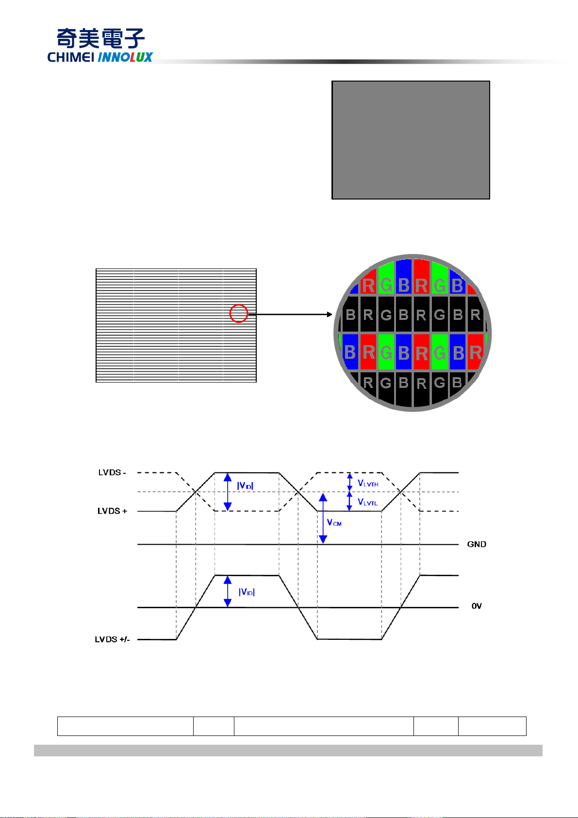
Item Specification Unit Note
Active Area
Bezel Opening Area
Driver Element
Pixel Number
Pixel Pitch(Sub Pixel)
Pixel Arrangement RGB vertical stripe - Display Colors 16.7M color Display Operation Mode Transmissive mode / Normally black - -
Surface Treatment
Rotation Function Unachievable
1095.84(H) x (V) 616.41 (50” diagonal)
1102.84(H) x 623.41(V)
a-si TFT active matrix
1920 x R.G.B. x 1080
0.1903(H) x 0.5708(V)
Anti-Glare coating (3.5% Low Haze)
mm
mm
- -
pixel -
mm -
- (2)
(3)
(1)
Display Orientation
Note (1) Please refer to the attached drawings in chapter 9 for more information about the front and back outlines.
Note (2) The spec of the surface treatment is temporarily for this phase. CMI reserves the rights to change this feature.
Version2.9 6 Date 21 June.2012
The copyright belongs to CHIMEI InnoLux. Any unauthorized use is prohibited
Signal input with “CMI”
(3)
Page 7

Tcon
Board
PRODUCT SPECIFICATION
Note (3)
Back Side
Front Side
CMI
Version2.9 7 Date 21 June.2012
The copyright belongs to CHIMEI InnoLux. Any unauthorized use is prohibited
Page 8
PRODUCT SPECIFICATION
1.5 MECHANICAL SPECIFICATIONS
Item Min. Typ. Max. Unit Note
Horizontal (H) 1121.14 1122.64 1124.14 mm Module Size
Vertical (V) 643.81 645.31 646.81 mm
Module Size
Weight
Note (1)Please refer to the attached drawings for more information of front and back outline dimensions.
Note (2) Module Depth does not include connectors.
Depth (D)
Weight
14.1 15.1 16.1 mm To Rear
23 24 25
14000
mm To converter
cover
Kg Weight
Version2.9 8 Date 21 June.2012
The copyright belongs to CHIMEI InnoLux. Any unauthorized use is prohibited
Page 9
PRODUCT SPECIFICATION
2. ABSOLUTE MAXIMUM RATINGS
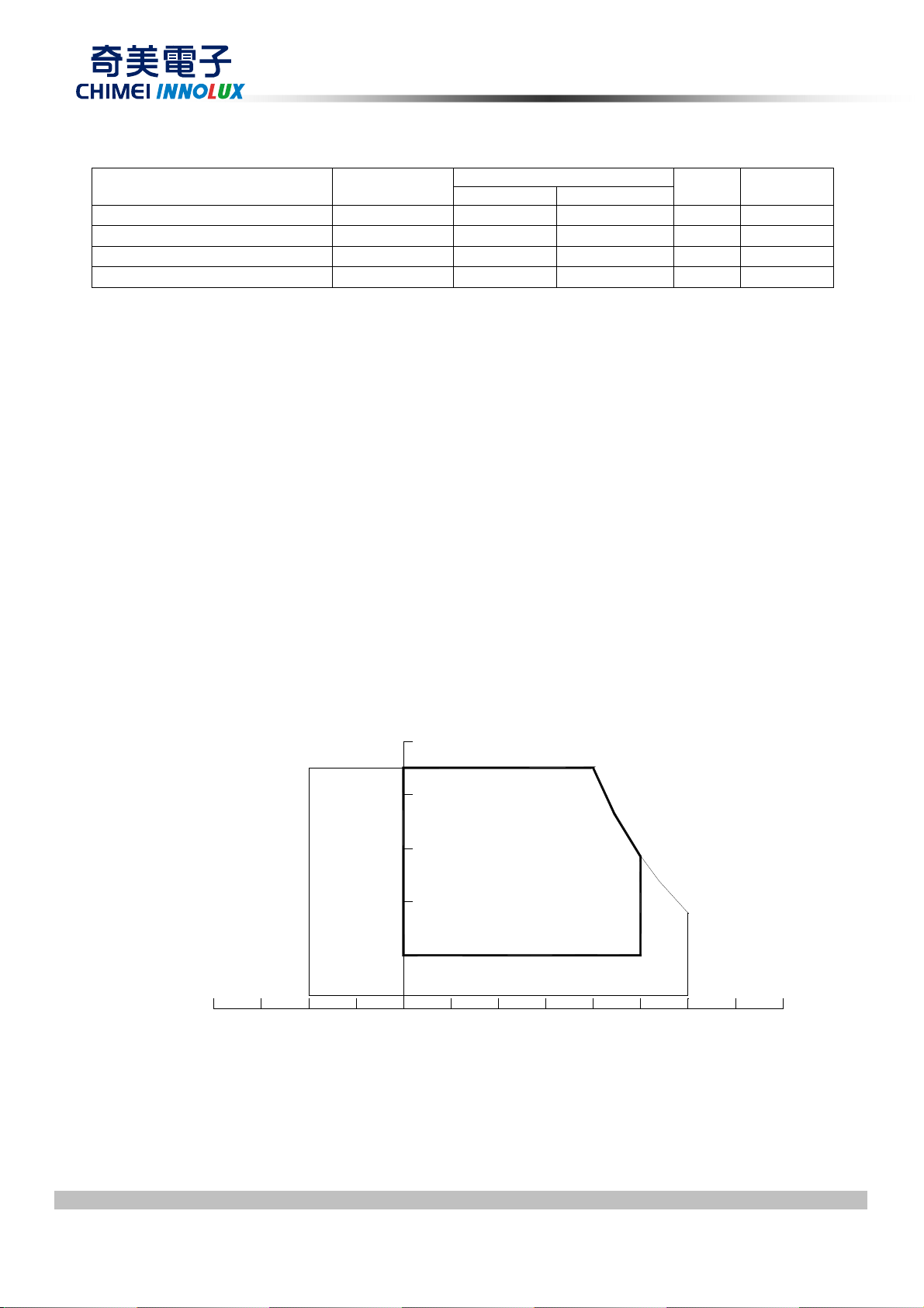
2.1 ABSOLUTE RATINGS OF ENVIRONMENT
Item Symbol
Storage Temperature TST -20 +60 ºC (1)
Operating Ambient Temperature TOP 0 50 ºC (1), (2)
Shock (Non-Operating) S
Vibration (Non-Operating) V
Note (1) Temperature and relative humidity range is shown in the figure below.
(a) 90 %RH Max. (Ta 40 ºC).≦
(b) Wet-bulb temperature should be 39 ºC Max. (Ta > 40 ºC).
(c) No condensation.
Note (2) The maximum operating temperature is based on the test condition that the surface temperature of
display area is less than or equal to 65 ºC with LCD module alone in a temperature controlled chamber.
Thermal management should be considered in final product design to prevent the surface temperature
of display area from being over 65 ºC. The range of operating temperature may degrade in case of
- 35 G (3), (5)
NOP
- 1.0 G (4), (5)
NOP
Min. Max.
Value
Unit Note
improper thermal management in final product design.
Note (3) 11 ms, half sine wave, 1 time for ± X, ± Y, ± Z.
Note (4) 10 ~ 200 Hz, 30 min, 1 time each X, Y, Z.
Note (5) At testing Vibration and Shock, the fixture in holding the module has to be hard and rigid enough so that
the module would not be twisted or bent by the fixture.
Relative Humidity (%RH)
100
90
80
60
Operating Range
40
20
10
Storage Range
Temperature (ºC)
80 60 -20 40 0 20 -40
Version2.9 9 Date 21 June.2012
The copyright belongs to CHIMEI InnoLux. Any unauthorized use is prohibited
Page 10
PRODUCT SPECIFICATION
2.2 PACKAGE STORAGE
When storing modules as spares for a long time, the following precaution is necessary.
(a) Do not leave the module in high temperature, and high humidity for a long time, It is highly recommended to
store the module with temperature from 0 to 35 ℃ at normal humidity without condensation.
(b) The module shall be stored in dark place. Do not store the TFT-LCD module in direct sunlight or fluorescent
light.
2.3 ELECTRICAL ABSOLUTE RATINGS
2.3.1 TFT LCD MODULE
Item Symbol
Min. Max.
Power Supply Voltage VCC -0.3 13.5 V
Logic Input Voltage VIN -0.3 3.6 V
Value
Unit Note
(1)
2.3.2 BACKLIGHT CONVERTER UNIT
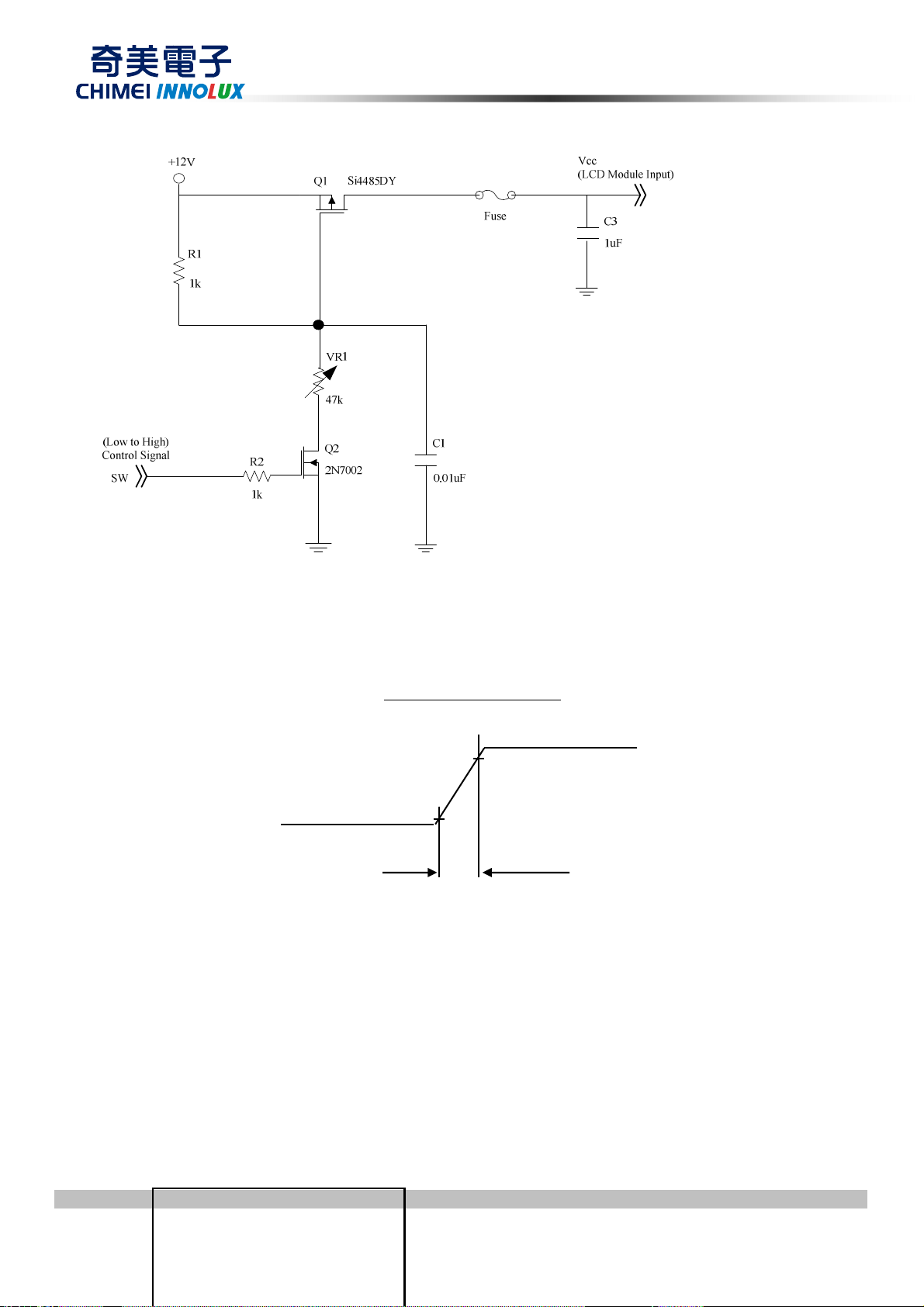
Item Symbol
Light Bar Voltage VW Ta = 25 ℃ - - 60 V
Converter Input Voltage VBL - 0 - 30 V
Control Signal Level - - -0.3
Note (1) Permanent damage to the device may occur if maximum values are exceeded. Function
operation should be restricted to the conditions described under Normal Operating Conditions.
Note (2) No moisture condensation or freezing.
Note (3) The control signals include On/Off Control and External PWM Control.
Test
Condition
Min. Type Max. Unit
RMS
- 6 V
3D Mode
Note
Version2.9 10 Date 21 June.2012
The copyright belongs to CHIMEI InnoLux. Any unauthorized use is prohibited
Page 11

PRODUCT SPECIFICATION
3. ELECTRICAL CHARACTERISTICS
3.1 TFT LCD MODULE
(Ta = 25 ± 2 ºC)
Value
Parameter Symbol
Min. Typ. Max.
Power Supply Voltage VCC 10.8 12 13.2 V (1)
Unit Note
Rush Current I
White Pattern P
Power Consumption
Power Supply
Current
Differential Input High
Threshold Voltage
Differential Input Low
LVDS
interface
CMIS
Threshold Voltage
Common Input Voltage VCM 1.0 1.2 1.4 V
Differential input voltage
(single-end)
Terminating Resistor RT
Input High Threshold Voltage VIH 2.7
Horizontal Stripe
Black Pattern PT
White Pattern
Horizontal Stripe
Black Pattern
RUSH
T
PT
- -
- -
- -
V
LVTH
V
LVTL
|VID| 200
- -
-
-
-
+100
-300
-
3.06 A (2)
7.2 8.6 W
15.8 19.0 W
7.3 8.7 W
0.6 0.72 A
1.3 1.6 A
0.61 0.73 A
-
-
-
100
-
+300 mV
-100 mV
600 mV
-
3.3 V
ohm
(3)
(4)
interface
Note (1) The module should be always operated within the above ranges.
The ripple voltage should be controlled under 10% of Vcc (Typ.)
Note (2) Measurement condition:
Version2.9 11 Date 21 June.2012
Input Low Threshold Voltage
The copyright belongs to CHIMEI InnoLux. Any unauthorized use is prohibited
VIL 0
-
0.7 V
Page 12
PRODUCT SPECIFICATION
GND
Vcc rising time is 470us
0.9Vcc
0.1Vcc
470us
Vcc
Note (3) The specified power consumption and power supply current is under the conditions at Vcc = 12 V, Ta =
25 ± 2 ºC, fv = 120 Hz, whereas a power dissipation check pattern below is displayed.
a. White Pattern
Version2.9 12 Date 21 June.2012
The copyright belongs to CHIMEI InnoLux. Any unauthorized use is prohibited
b. Black Pattern
Page 13
PRODUCT SPECIFICATION
c. Horizontal Pattern
Active Area
Note (4) The LVDS input characteristics are as follows:
3.2 BACKLIGHT UNIT
3.2.1 LED LIGHT BARCHARACTERISTICS (Ta = 25 ± 2 ºC)
Parameter Symbol
Version2.9 13 Date 21 June.2012
The copyright belongs to CHIMEI InnoLux. Any unauthorized use is prohibited
Value
Unit Note
Page 14
PRODUCT SPECIFICATION
Min. Typ. Max.
Total Current (16 String) If
I
L(2D)
- 1840 1952
- 115
122
mA
mA
One String Current
I
L(3D)
LED Forward Voltage Vf
One String Voltage VW
One String Voltage Variation V△W
Life time -
- 400 424
5.5 6.15 7
44 - 56
- - 2
30,000 - -
mApeak 3D ENA=ON
VDC IL =115mA
VDC IL =115mA
V
Hrs (1)
Note (1) The lifetime is defined as the time which luminance of the LED decays to 50% compared to the initial
value, Operating condition: Continuous operating at Ta = 25±2 , I℃L =115mA.
3.2.2 CONVERTER CHARACTERISTICS (Ta = 25 ± 2 ºC)
Value
Parameter Symbol
Unit
Note
Min. Typ. Max.
(1), (2)
P
BL(2D)
-
87.3 100.4
W
IL = 115mA
Power Consumption
(1), (2)
P
BL(3D)
-
85 96
W
IL=400mA.
Converter Input Voltage VBL 22.8 24.0 25.2 VDC
-
I
BL(2D)
3.64 4.2
A
Non Dimming
Converter Input Current
-
I
BL(3D)
3.54 4
A
VBL=22.8V,(IL=typ.)
I
-
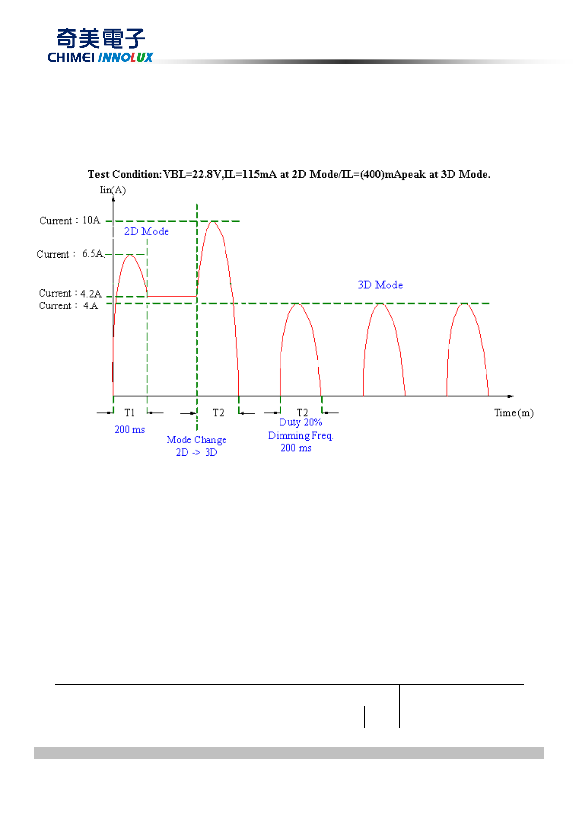
R(2D)
- 6.5
Apeak
(3), (6)
Input Inrush Current
VBL=22.8V,(IL=
I
- - 10 Apeak
Dimming Frequency
Dimming Duty Ratio
R(3D)
FB 170 180 190 Hz
DDR 5 - 100 %
360mA.)(3), (6)
(5)
(4), (5)
Note (1) The power supply capacity should be higher than the total converter power consumption PBL. Since
the pulse width modulation (PWM) mode was applied for backlight dimming, the driving current
changed as PWM duty on and off. The transient response of power supply should be considered
for the changing loading when converter dimming.
Note (2) The measurement condition of Max. value is based on 50" backlight unit under input voltage 24V,
average LED current 122 mA at 2D Mode (LED current 424 mA
at 3D Mode) and lighting 1 hour
peak
later.
Note (3) For input inrush current measure, the VBL rising time from 10% to 90% is about 30ms.
Version2.9 14 Date 21 June.2012
The copyright belongs to CHIMEI InnoLux. Any unauthorized use is prohibited
Page 15
PRODUCT SPECIFICATION
Note (4) EPWM signal have to input available duty range. Between 97% and 100% duty(DDR) have to be
avoided. (97% < DDR < 100%) But 100% duty(DDR) is possible. 5% duty(DDR) is only valid for
electrical operation.
Note (5) FB and DDR are available only at 2D Mode.
Note (6) Below diagram is only for power supply design reference.
3.2.3 CONVERTER INTERFACE CHARACTERISTICS
Test
Parameter Symbol
Condition
Value
Unit Note
Min. Typ. Max.
Version2.9 15 Date 21 June.2012
The copyright belongs to CHIMEI InnoLux. Any unauthorized use is prohibited
Page 16
PRODUCT SPECIFICATION
ON
On/Off Control Voltage
OFF
External PWM Control
Voltage
External PWM Frequency
Error Signal ERR
VBL Rising Time Tr1
Control Signal Rising Time Tr
Control Signal Falling Time Tf
PWM Signal Rising Time TPWMR
PWM Signal Falling Time TPWMF
HI
LO
VBLON
VEPWM
F
EPWM
-
-
-
-
- 150 160 170 Hz
- - - - -
-
- - -
- - -
- - -
- - -
2.0
0
2.0
0
20
-
-
-
-
- -
5.0 V
0.8 V
5.25
0.8 V Duty off
100 ms
100 ms
50 us
50 us
V Duty on
(5), (6)
Normal mode
(7)
Abnormal: Open
collector Normal:
GND
(4)
ms 10%-90%VBL
(6)
Input Impedance Rin
PWM Delay Time TPWM
Ton
BLON Delay Time
T
on1
BLON Off Time Toff
Note (1) The Dimming signal should be valid before backlight turns on by BLON signal. It is inhibited to
change the external PWM signal during backlight turn on period.
Note (2) The power sequence and control signal timing are shown in the Fig.1. For a certain reason, the
converter has a possibility to be damaged with wrong power sequence and control signal timing.
Note (3) While system is turned ON or OFF, the power sequences must follow as below descriptions:
Turn ON sequence: VBL → PWM signal → BLON
Turn OFF sequence: BLOFF → PWM signal → VBL
Note (4) When converter protective function is triggered, ERR will output open collector status. Please refers to
Fig.2.
Note (5) The EPWM interface that inserts a pull up resistor to 5V in Max Duty (100%), please refers to Fig.3.
-
-
-
-
-
1
100
300
300
300
- -
- -
- -
- -
- -
MΩ
ms (6)
ms
ms
ms
EPWM, BLON
Note (6) EPWM is available only at 2D Mode.
Note (7) EPWM signal have to input available frequency range.
Note (8) [Recommend] EPWM duty ratio is set at 100%(Max. Brightness) in 3D Mode.
Version2.9 16 Date 21 June.2012
The copyright belongs to CHIMEI InnoLux. Any unauthorized use is prohibited
Page 17

PRODUCT SPECIFICATION
V
V
BL
V
BLON
EPWM
Tr1
BL
0.9V
0.1V
BL
2.0V
0.8V
Ton
Ton1
0
0
Toff
Backlight on duration
Tr
Tf
Ext. Dimming Function
PWMR
T
2.0V
0
0.8V
T
PWM
T
PWMF
Floating
V
W
External
PWM
Period
External
PWM Duty
100%
Fig. 1
Fig. 2
Version2.9 17 Date 21 June.2012
The copyright belongs to CHIMEI InnoLux. Any unauthorized use is prohibited
Page 18

EPWM
5V +/- 5%
Converter
Side
10kΩ
Ω
ΩΩ
>1MΩ
Ω
ΩΩ
Fig. 3
PRODUCT SPECIFICATION
10kΩ
Ω
ΩΩ
Dimming
Circuit
Version2.9 18 Date 21 June.2012
The copyright belongs to CHIMEI InnoLux. Any unauthorized use is prohibited
Page 19
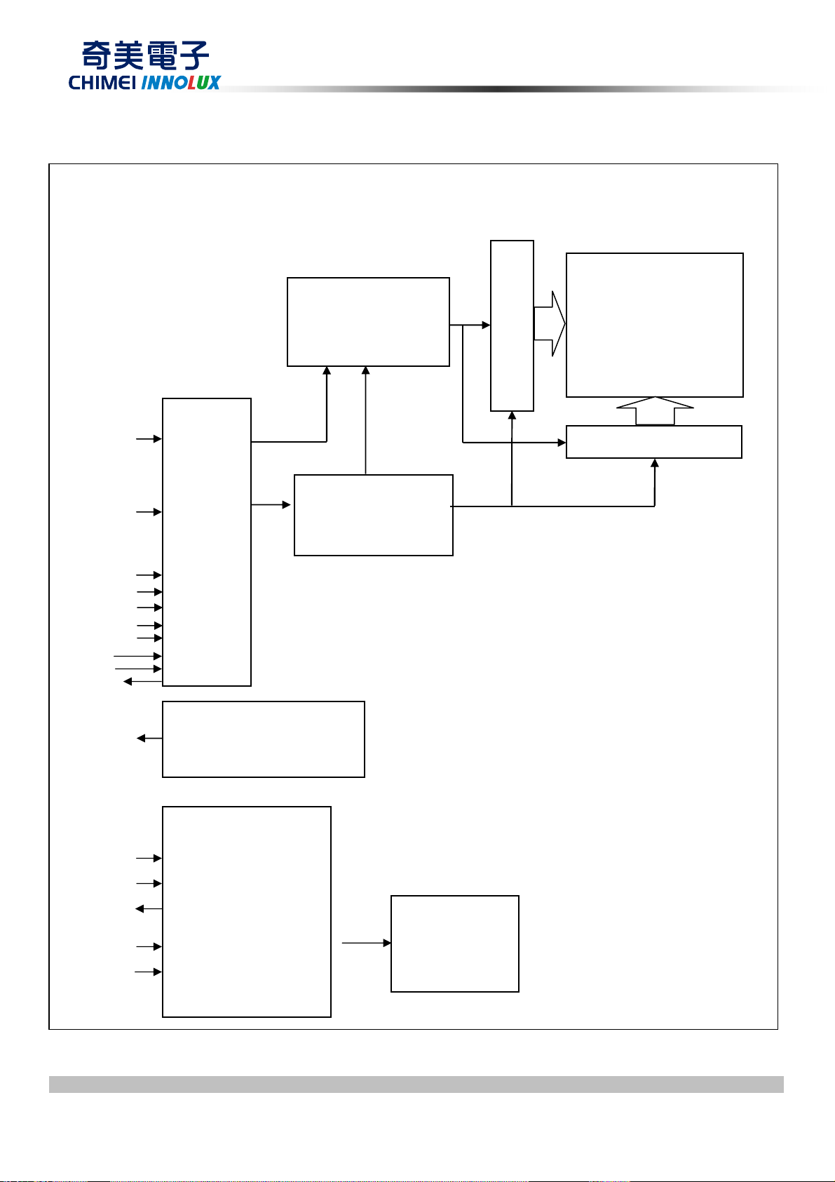
4. BLOCK DIAGRAM OF INTERFACE
E_PWM
ERR
DATA DRIVER
SCAN DRIVER
GND
SEL
LVDS
LR
LD_EN
L/R_O
SCN_EN
4.1 TFT LCD MODULE
PRODUCT SPECIFICATION
CH1_0(+/-)
CH1_1(+/-)
CH1_2(+/-)
CH1_3(+/-)
CH1_CLK(+/-)
CH2_0(+/-)
CH2_1(+/-)
CH2_2(+/-)
CH2_3(+/-)
CH2_CLK(+/-)
2D/3D
VCC
L/R_O
2
nd
:GS13512-1421S-7H-FOXCONN
1
INPUT CONNECTOR
st
:WF23-400-513C-FCN
TIMING
CONTROLLER
DC/DC CONVERTER
TFT LCD PANEL
(1920x3x1080)
& REFERENCE VOLTAGE
OUTPUT CONNECTOR
CN1:LM123S-010-H-TF1-3
CONVERTER
VBL
GND
BLON
CONNECTOR
CN1:
CI0114M1HR0-LA
(CvilLux)
CN2&CN3: 196389-08041-3 (P-TWO)
LED BACKLIGHT
UNIT
Version2.9 19 Date 21 June.2012
The copyright belongs to CHIMEI InnoLux. Any unauthorized use is prohibited
Page 20

PRODUCT SPECIFICATION
Input signal for Left Right eye frame synchronous(Frame sequence
5 .INPUT TERMINAL PIN ASSIGNMENT
5.1 TFT LCD MODULE
CNF1 Connector Part No.: FCN (WF23-400-513C)
Pin Name Description Note
1 N.C. No Connection (1)
2 SCL I2C Serial Clock (for 3D format selection function)
3 SDA I2C Serial Data (for 3D format selection function)
4 N.C. No Connection (1)
5 L/R_O Output signal for Left Right Glasses control (10)
6 N.C. No Connection (1)
7 SELLVDS Input signal for LVDS Data Format Selection (2)(7)
8 N.C. No Connection
(11)
9 N.C. No Connection
10 N.C. No Connection
11 GND Ground
12 ORX0- Odd pixel Negative LVDS differential data input. Channel 0
13 ORX0+ Odd pixel Positive LVDS differential data input. Channel 0
14 ORX1- Odd pixel Negative LVDS differential data input. Channel 1
15 ORX1+ Odd pixel Positive LVDS differential data input. Channel 1
16 ORX2- Odd pixel Negative LVDS differential data input. Channel 2
17 ORX2+ Odd pixel Positive LVDS differential data input. Channel 2
18 GND Ground
19 OCLK- Odd pixel Negative LVDS differential clock input
20 OCLK+ Odd pixel Positive LVDS differential clock input
21 GND Ground
22 ORX3- Odd pixel Negative LVDS differential data input. Channel 3
23 ORX3+ Odd pixel Positive LVDS differential data input. Channel 3
(1)
(9)
(9)
(9)
24 N.C. No Connection
25 N.C. No Connection
26 2D/3D Input signal for 2D/3D Mode Selection (3)(6)(8)
27 L/R
Version2.9 20 Date 21 June.2012
The copyright belongs to CHIMEI InnoLux. Any unauthorized use is prohibited
mode)
(1)
(4)(8)
Page 21

PRODUCT SPECIFICATION
28 ERX0- Even pixel Negative LVDS differential data input. Channel 0
29 ERX0+ Even pixel Positive LVDS differential data input. Channel 0
30 ERX1- Even pixel Negative LVDS differential data input. Channel 1
(9)
31 ERX1+ Even pixel Positive LVDS differential data input. Channel 1
32 ERX2- Even pixel Negative LVDS differential data input. Channel 2
33 ERX2+ Even pixel Positive LVDS differential data input. Channel 2
34 GND Ground
35 ECLK- Even pixel Negative LVDS differential clock input.
(9)
36 ECLK+ Even pixel Positive LVDS differential clock input.
37 GND Ground
38 ERX3- Even pixel Negative LVDS differential data input. Channel 3
(9)
39 ERX3+ Even pixel Positive LVDS differential data input. Channel 3
40 N.C. No Connection
(1)
41 N.C. No Connection
42 LD_EN Input signal for Local Dimming Enable (5)(8)
43 SCN_EN Input signal for Scanning Enable (6)(8)
44 GND Ground
45 GND Ground
46 GND Ground
47 N.C. No Connection (1)
48 VCC +12V power supply
49 VCC +12V power supply
50 VCC +12V power supply
51 VCC +12V power supply
Version2.9 21 Date 21 June.2012
The copyright belongs to CHIMEI InnoLux. Any unauthorized use is prohibited
Page 22

CN1 Connector Pin Assignment LM123S-010-H-TF1-3 (UNE)
SELLVDS
Note
L JEIDA Format
H or Open
VESA Format
2D/3D
Note
L or Open
2D
Mode
H 3D Mode
L/R Note
L Right synchronous signal
H Left synchronous signal
1 N.C. No Connection
PRODUCT SPECIFICATION
2 N.C. No Connection
3 N.C. No Connection
4 GND Ground
5 N.C. No Connection
6 L/R_O Output signal for Left Right Glasses control
7 N.C. No Connection
8 N.C. No Connection
9 N.C. No Connection
10 N.C. No Connection
Note (1) Reserved for internal use. Please leave it open.
Note (2) LVDS format selection.
L= Connect to GND, H=Connect to +3.3V or Open
(1)
(1)
(10)
(1)
Note (3) 2D/3D mode selection.
L= Connect to GND or Open, H=Connect to +3.3V
Note (4) Input signal for Left Right eye frame synchronous
VIL=0~0.8 V, VIH=2.0~3.3 V
Version2.9 22 Date 21 June.2012
The copyright belongs to CHIMEI InnoLux. Any unauthorized use is prohibited
Page 23
PRODUCT SPECIFICATION
L Local Dimming Disable
H or Open
Local Dimming Enable
L or Open
Scanning Disable
H Scanning Enable
Note (5) Local dimming enable selection.
L= Connect to GND, H=Connect to +3.3V or Open
LD_EN Note
LD_EN enable pin should be set in power on stage.
Backlight should be turned off in the period of changing original setting after power on.
Note (6) Scanning enable selection.
L= Connect to GND or Open, H=Connect to +3.3V
SCN_EN Note
Note (7) Interface optional pin has internal scheme as following diagram.
Customer should keep the interface voltage level requirement which including Panel board loading as
below.
3.3V
Panel Board System Board
>16K ohm
1K ohm
IC
Interface Voltage Level
VH > V
IH
VL < V
IL
Note (8) Interface optional pin has internal scheme as following diagram.
Version2.9 23 Date 21 June.2012
The copyright belongs to CHIMEI InnoLux. Any unauthorized use is prohibited
Page 24

PRODUCT SPECIFICATION
L Right glass turn on
H Left glass turn on
Customer should keep the interface voltage level requirement which including Panel board loading as
below.
Panel Board System Board
1K ohm
IC
>16K ohm
Interface Voltage Level
VH > V
IH
VL < V
IL
Note (9) Two pixel data send into the module for every clock cycle. The first pixel of the frame is odd pixel and
the second pixel is even pixel.
Note (10) The definition of L/R_O signal as follows
L= 0V , H= +3.3V
L/R_O Note
Note (11) Please reference Appendix A
Note (12) Currently, we only support line alternative format (1st line is left signal), show as the attached block
diagram. In the future, we will support other format.
L
R
L
R
.
.
.
.
Line alternative format
Note (13) LVDS connector pin order defined as follows
Version2.9 24 Date 21 June.2012
The copyright belongs to CHIMEI InnoLux. Any unauthorized use is prohibited
Page 25

PRODUCT SPECIFICATION
5.2 BACKLIGHT UNIT
The pin configuration for the housing and leader wire is shown in the table below.
CN2,3,6,7: 196388-12041-3 (P-TWO)
Pin № Symbol Feature
1 VLED
2 VLED
3 VLED
4 VLED
5 NC
6 NC
7 NC
8 NC
9 N1
10 N2
11 N3
12 N4
Positive of LED String
NC
Negative of LED String
5.3 CONVERTER UNIT
CN1(Header): CI0114M1HR0-LA (CvilLux)
Version2.9 25 Date 21 June.2012
The copyright belongs to CHIMEI InnoLux. Any unauthorized use is prohibited
Page 26

PRODUCT SPECIFICATION
Pin No. Symbol Feature
1
2
3
4
5
6
7
8
9
10
11 ERR
12 BLON BL ON/OFF
13 NC NC
14 E_PWM
Note (1) If Pin14 is open, E_PWM is 100% duty.
Note (2) Input connector pin order defined as follows
VBL +24V
GND GND
Normal (GND)
Abnormal (Open
External PWM
Control
5.4 LVDS INTERFACE
JEIDA Format : SELLVDS = L
VESA Format : SELLVDS = H or Open
VESA LVDS format
Version2.9 26 Date 21 June.2012
The copyright belongs to CHIMEI InnoLux. Any unauthorized use is prohibited
Page 27

RXCLK±
RXCLK±
PRODUCT SPECIFICATION
Current cycle
Current cycle
ORX0±
ORX0±
ORX1±
ORX1±
ORX2±
ORX2±
ORX3±
ORX3±
ERX0±
ERX0±
ERX1±
ERX1±
ERX2±
ERX2±
ERX3±
ERX3±
JEDIA LVDS format
RXCLK±
RXCLK±
R5G0 R4 R3 R2 R1
R5G0 R4 R3 R2 R1
B0 G5B1
B0 G5B1
R5G0 R4 R3 R2 R1
R5G0 R4 R3 R2 R1
B0 G5B1
B0 G5B1
Current cycle
Current cycle
G3 G2G4
G3 G2G4
G3 G2G4
G3 G2G4
R0
R0
G1
G1
B2B4 B3B5VS HSDE
B2B4 B3B5VS HSDE
R6G6 R7G7B7 B6RSVD
R6G6 R7G7B7 B6RSVD
R0
R0
G1
G1
B2B4 B3B5VS HSDE
B2B4 B3B5VS HSDE
R6G6 R7G7B7 B6RSVD
R6G6 R7G7B7 B6RSVD
ORX0±
ORX0±
ORX1±
ORX1±
ORX2±
ORX2±
ORX3±
ORX3±
ERX0±
ERX0±
ERX1±
ERX1±
ERX2±
ERX2±
ERX3±
ERX3±
R7G2 R6 R5 R4 R3
R7G2 R6 R5 R4 R3
B2 G7B3
B2 G7B3
R7G2 R6 R5 R4 R3
R7G2 R6 R5 R4 R3
B2 G7B3
B2 G7B3
G5 G4G6
G5 G4G6
G5 G4G6
G5 G4G6
R2
R2
G3
G3
B4B6 B5B7VS HSDE
B4B6 B5B7VS HSDE
R0G0 R1G1B1 B0RSVD
R0G0 R1G1B1 B0RSVD
R2
R2
G3
G3
B4B6 B5B7VS HSDE
B4B6 B5B7VS HSDE
R0G0 R1G1B1 B0RSVD
R0G0 R1G1B1 B0RSVD
5.5 COLOR DATA INPUT ASSIGNMENT
The brightness of each primary color (red, green and blue) is based on the 8-bit gray scale data input for the color. The higher
the binary input, the brighter the color. The table below provides the assignment of the color versus data input.
Version2.9 27 Date 21 June.2012
The copyright belongs to CHIMEI InnoLux. Any unauthorized use is prohibited
Page 28

PRODUCT SPECIFICATION
Data Signal
Basic
Colors
Gray
Scale
Of
Red
Color
Black
Red
Green
Blue
Cyan
Magenta
Yellow
White
Red (0) / Dark
Red (1)
Red (2)
:
:
Red (253)
Red (254)
Red Green Blue
R7 R6 R5 R4 R3 R2 R1 R0 G7 G6 G5 G4 G3 G2 G1 G0 B7 B6 B5 B4 B3 B2 B1 B0
0
0
0
0
0
0
0
0
0
0
0
0
0
0
0
0
0
0
0
0
0
0
0
1
1
1
1
1
1
1
1
0
0
0
0
0
0
0
0
0
0
0
0
0
0
0
0
0
0
0
0
0
0
0
1
1
1
1
1
1
1
1
0
0
0
0
0
0
0
0
0
0
0
0
0
0
0
0
0
0
0
0
0
0
0
1
1
1
1
1
1
1
0
0
0
0
0
0
0
0
1
1
1
1
1
1
1
1
1
1
1
1
1
1
1
1
1
1
1
1
1
1
1
0
0
0
0
0
0
0
0
1
1
1
1
1
1
1
1
1
1
1
1
1
1
1
1
1
1
1
1
1
1
1
0
0
0
0
0
0
0
1
1
1
1
1
1
1
1
1
1
1
1
1
1
1
1
1
1
1
1
1
1
1
0
0
0
0
0
0
0
0
0
0
0
0
0
0
0
0
0
0
0
0
0
0
0
0
0
0
0
0
0
0
1
0
0
0
0
0
0
0
0
0
0
0
0
0
0
0
0
0
0
0
0
0
1
0
0
0
0
0
0
0
0
0
0
0
0
0
0
0
0
:
:
:
:
:
:
:
:
:
:
:
:
:
:
:
:
:
:
:
:
:
:
:
:
:
:
:
:
:
:
:
:
:
:
:
:
:
:
:
:
:
:
:
:
:
:
1
1
1
1
1
1
0
1
0
0
0
0
0
0
0
0
0
0
0
0
0
0
0
1
1
1
1
1
1
1
0
0
0
0
0
0
0
0
0
0
0
0
0
0
0
0
0
0
0
1
1
1
0
1
0
0
0
:
:
0
0
Gray
Scale
Of
Green
Gray
Scale
Of
Blue
Red (255)
Green (0) / Dark
Green (1)
Green (2)
:
:
Green (253)
Green (254)
Green (255)
Blue (0) / Dark
Blue (1)
Blue (2)
:
:
Blue (253)
Blue (254)
Blue (255)
1
1
1
1
1
1
1
1
0
0
0
0
0
0
0
0
0
0
0
0
0
0
0
0
0
0
0
0
0
0
0
0
0
0
0
0
0
0
0
0
0
0
0
0
0
0
0
0
0
0
0
0
0
0
0
0
0
0
0
0
0
0
0
1
0
0
0
0
0
0
0
0
0
0
0
0
0
0
0
0
0
0
0
0
0
0
1
0
0
0
0
0
0
0
0
0
:
:
:
:
:
:
:
:
:
:
:
:
:
:
:
:
:
:
:
:
:
:
:
:
:
:
:
:
:
:
:
:
:
:
:
:
:
:
:
:
:
:
:
:
:
:
:
:
0
0
0
0
0
0
0
0
1
1
1
1
1
1
0
1
0
0
0
0
0
0
0
0
0
0
0
0
0
0
0
0
1
1
1
1
1
1
1
0
0
0
0
0
0
0
0
0
0
0
0
0
0
0
0
0
1
1
1
1
1
1
1
1
0
0
0
0
0
0
0
0
0
0
0
0
0
0
0
0
0
0
0
0
0
0
0
0
0
0
0
0
0
0
0
0
0
0
0
0
0
0
0
0
0
0
0
0
0
0
0
0
0
0
0
0
0
0
0
1
0
0
0
0
0
0
0
0
0
0
0
0
0
0
0
0
0
0
0
0
0
0
1
0
:
:
:
:
:
:
:
:
:
:
:
:
:
:
:
:
:
:
:
:
:
:
:
:
:
:
:
:
:
:
:
:
:
:
:
:
:
:
:
:
:
:
:
:
:
:
:
:
0
0
0
0
0
0
0
0
0
0
0
0
0
0
0
0
1
1
1
1
1
1
0
1
0
0
0
0
0
0
0
0
0
0
0
0
0
0
0
0
1
1
1
1
1
1
1
0
0
0
0
0
0
0
0
0
0
0
0
0
0
0
0
0
1
1
1
1
1
1
1
1
Note (1) 0: Low Level Voltage, 1: High Level Voltage
Version2.9 28 Date 21 June.2012
The copyright belongs to CHIMEI InnoLux. Any unauthorized use is prohibited
Page 29

PRODUCT SPECIFICATION
Version2.9 29 Date 21 June.2012
The copyright belongs to CHIMEI InnoLux. Any unauthorized use is prohibited
Page 30

PRODUCT SPECIFICATION
6. INTERFACE TIMING
6.1 INPUT SIGNAL TIMING SPECIFICATIONS
The input signal timing specifications are shown as the following table and timing diagram. (Ta = 25 ± 2 ºC)
Signal Item Symbol
Frequency
Input cycle to
LVDS
cycle jitter
Receiver
Spread spectrum
Clock
modulation range
Spread spectrum
modulation frequency
LVDS
Receiver
Receiver Skew Margin T
Data
6.1.1 Timing spce for Frame Rate = 50Hz
Signal Item Symbol
2D mode Fr5 47 50 53 Hz (8),(9)
Frame rate
3D mode Fr5 50 50 50 Hz (6),(8),(9)
Min. Typ. Max. Unit Note
F
clkin
60 74.25 77 MHz
(=1/TC)
T
- - 200 ps (2)
rcl
F
clkin_mod
F
F
SSM
RSKM
-2%
clkin
- - 200 KHz
-400 - 400 ps (4)
- F
clkin
+2%
MHz
Min. Typ. Max. Unit Note
(3)
Total Tv 1115 1125 1380 Th Tv=Tvd+Tvb
Vertical
Active
Display
Term
2D Mode
3D Mdoe
Display Tvd 1080 1080 1080 Th
Blank Tvb 35 45 300 Th
Total Tv 1350 Th
Display Tvd 1080 Th
-
-
(5), (7)
Blank Tvb 270 Th
Total Th 1050 1100 1150 Tc Th=Thd+Thb
Horizontal
Active
Display
Term
2D Mode
3D Mdoe
Display Thd 960 960 960 Tc
Blank Thb 90 140 190 Tc
Total Th 1050 1100 1150 Tc Th=Thd+Thb
Display Thd 960 960 960 Tc
Blank Thb 90 140 190 Tc
-
-
-
-
6.1.2 Timing spec for Frame Rate = 60Hz
Version2.9 30 Date 21 June.2012
The copyright belongs to CHIMEI InnoLux. Any unauthorized use is prohibited
Page 31

PRODUCT SPECIFICATION
Signal Item Symbol
2D mode Fr6 57 60 62.5 Hz (8),(9)
Frame rate
3D mode Fr6 60 60 60 Hz (6),(8),(9)
Total Tv 1115 1125 1380 Th Tv=Tvd+Tvb
Vertical
Active
Display
Term
2D Mode
3D Mdoe
Display Tvd 1080 1080 1080 Th
Blank Tvb 35 45 300 Th
Total Tv 1125 Th
Display Tvd 1080 Th
Blank Tvb 45 Th
Total Th 1050 1100 1150 Tc Th=Thd+Thb
Horizontal
Active
Display
Term
2D Mode
3D Mdoe
Display Thd 960 960 960 Tc
Blank Thb 90 140 190 Tc
Total Th 1050 1100 1150 Tc Th=Thd+Thb
Display Thd 960 960 960 Tc
Min. Typ. Max. Unit Note
-
-
(5), (7)
-
-
-
Blank Thb 90 140 190 Tc
Note (1) Please make sure the range of pixel clock has follow the below equation:
F
clkin(max)
F
r
5
Tv Th F╳ ╳ ≧
F≧
r
6
Tv Th╳ ╳
clkin(min)
-
INPUT SIGNAL TIMING DIAGRAM
Version2.9 31 Date 21 June.2012
The copyright belongs to CHIMEI InnoLux. Any unauthorized use is prohibited
Page 32

PRODUCT SPECIFICATION
Vtotal
VS
HS
DE
VBP VFP Vdisplay
•
VBP max : 150 line
Suggest VBP = VFP = ½ * (Vtotal - Vdisplay)
Version2.9 32 Date 21 June.2012
The copyright belongs to CHIMEI InnoLux. Any unauthorized use is prohibited
Page 33

PRODUCT SPECIFICATION
Thb
Tc
DE
DCLK
DE
DATA
Th
Tvd
Tv
Tvb
Thd
Valid display data ( 960 clocks)
Note (2) The input clock cycle-to-cycle jitter is defined as below figures. Trcl = I T1 – TI
Version2.9 33 Date 21 June.2012
The copyright belongs to CHIMEI InnoLux. Any unauthorized use is prohibited
Page 34

PRODUCT SPECIFICATION
Note (3) The SSCG (Spread spectrum clock generator) is defined as below figures.
Note (4) LVDS receiver skew margin is defined and shown as below.
LVDS RECEIVER INTERFACE TIMING DIAGRAM
RXCLK+/-
RXn+/-
T
RSKM
Tc
Note (5) Please fix the Vertical timing (Vertical Total =1350 / Display =1080 / Blank = 270) in 50Hz 3D mode
and Vertical timing (Vertical Total =1125 / Display =1080 / Blank = 45) in 60Hz 3D mode
Note (6) In 3D mode, the set up Fr5 and Fr6 in Typ. ±3 Hz .In order to ensure that the electric function performance
to avoid no display symptom.(Except picture quality symptom.)
Note (7) In 3D mode, the set up Tv and Tvb in Typ. ±30.In order to ensure that the electric function performance to
avoid no display symptom.(Except picture quality symptom.)
Note (8) The frame-to-frame jitter of the input frame rate is defined as the above figures. FRn = FRn-1 ± 1.8%.
Note (9) The setup of the frame rate jitter > 1.8% may result in the cosmetic LED backlight symptom but the electric
function is not affected.
Version2.9 34 Date 21 June.2012
The copyright belongs to CHIMEI InnoLux. Any unauthorized use is prohibited
Page 35

PRODUCT SPECIFICATION
Version2.9 35 Date 21 June.2012
The copyright belongs to CHIMEI InnoLux. Any unauthorized use is prohibited
Page 36

PRODUCT SPECIFICATION
P
100ms
T6
6.2 POWER ON/OFF SEQUENCE
To prevent a latch-up or DC operation of LCD module, the power on/off sequence should be as the diagram
below.
0.5≦T1≦10ms
0≦T2
500ms ≦T4
≦200ms
0≦T3
0V
0.1VCC
T3 T1
T2
0.1Vcc
T4
LVDS Signals
0V
Power On
0≦T7≦T2
0≦T8≦T3
Option Signals
(SELLVDS,2D/3D
L/R,LD_EN, SCN_EN)
T7
T8
Backlight (Recommended)
500ms≦T5
≦
50%
T5
50%
T6
Version2.9 36 Date 21 June.2012
The copyright belongs to CHIMEI InnoLux. Any unauthorized use is prohibited
Page 37

PRODUCT SPECIFICATION
Scalar send
6.3
2D/3D MODE CHANGE SIGNAL SEQUENCE WITHOUT VCC TURN OFF AND TURN ON
VCC
0V
0.9VCC
0.1VCC
0.5≦T
1
0≦T
≦
2
≦
LVDS Signals
0≦T7≦T2
0≦T10≦10m
2D/3D
0≦T9≦10ms
10≦T12≦20ms
Scalar Black Pattern Insertion
10ms
50ms
0V
Power On
T7
T1
T2
T9
Black Pattern
T10
T12
Backlight ON/OFF
500ms≦T5
700ms≦T11
T5
T11
Note (1) The supply voltage of the external system for the module input should follow the definition of Vcc.
Note (2) Apply the LED voltage within the LCD operation range. When the backlight turns on before the LCD
operation or the LCD turns off before the backlight turns off, the display may momentarily become
abnormal screen.
Note (3) In case of Vcc is in off level, please keep the level of input signals on the low or high impedance. If
T2<0,that maybe cause electrical overstress failure.
Note (4) T4 should be measured after the module has been fully discharged between power off and on period.
Note (5) Interface signal shall not be kept at high impedance when the power is on.
Note (6) When 2D/3D mode is changed, TCON will insert black pattern internally. During black insertion, TCON
would load required optical table and TCON parameter setting. The black insertion time should be longer
than 650ms because TCON must recognize 2D or 3D format and set the correct parameter.
Version2.9 37 Date 21 June.2012
The copyright belongs to CHIMEI InnoLux. Any unauthorized use is prohibited
Page 38

PRODUCT SPECIFICATION
7. OPTICAL CHARACTERISTICS
7.1 TEST CONDITIONS
Item Symbol Value Unit
Ambient Temperature Ta
Ambient Humidity Ha
Supply Voltage VCC
Input Signal According to typical value in "3. ELECTRICAL CHARACTERISTICS"
LED Current IL
The LCD module should be stabilized at given temperature for 1 hour to avoid abrupt temperature change during
measuring in a windless room.
Local Dimming Function should be Disable before testing to get the steady optical characteristics (According to
5.1 CNF1 Connector Pin Assignment, Pin no. “42”)
25±2
50±10
12±1.2
115±3.45
o
C
%RH
V
mA
Version2.9 38 Date 21 June.2012
The copyright belongs to CHIMEI InnoLux. Any unauthorized use is prohibited
Page 39

PRODUCT SPECIFICATION
Center Luminance of
7.2 OPTICAL SPECIFICATIONS
The relative measurement methods of optical characteristics are shown in 7.2. The following items should be
measured under the test conditions described in 7.1 and stable environment shown in 7.1.
Item Symbol Condition Min. Typ. Max. Unit Note
Contrast Ratio CR
3500 5000
Response Time Gray to gray
280 350
White
White Variation
2D
L
C
3D
δW
2D
Cross Talk CT
3D-W
3D-D
θ
=0°, θY =0°
Red
Rx
Ry
x
Viewing angle at
normal direction
Gx
Green
Gy
Typ.-
Bx
Color
Blue
0.03
By
Chromaticity
Wx
White
Wy
- - Note (2)
6.5 13
- cd/m
85 - cd/m
ms Note (3)
2
Note (4)
2
Note (8)
1.3 - Note (6)
- 4 % Note (5)
4 - % Note (8)
11 - % Note (8)
0.644
0.330
0.296
0.595
-
-
-
-
Typ.+
0.148
-
0.03
0.054
0.280
0.290
-
-
-
Correlated color temperature
Color
Gamut
Horizontal
Viewing
Angle
Vertical
Transmission direction of
the up polarizer
C.G.
θ
+
x
θ
-
x
θ
+
Y
θ
-
Y
Φ
up
9800
-
80 88
80 88
72
- % NTSC
-
-
CR≥20
80 88
80 88
- - 90
-
-
-
K
Deg.
Deg.
(1)
(7)
Version2.9 39 Date 21 June.2012
The copyright belongs to CHIMEI InnoLux. Any unauthorized use is prohibited
Page 40
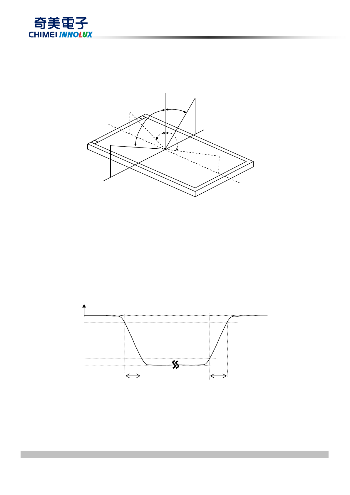
Note (1) Definition of Viewing Angle (θx, θy) :
T
ime
Viewing angles are measured by Autronic Conoscope Cono-80.
PRODUCT SPECIFICATION
θ
X-
= 90º
x-
6 o’clock
θ
y-
= 90º
y-
Note (2) Definition of Contrast Ratio (CR) :
The contrast ratio can be calculated by the following expression.
Contrast Ratio (CR) =
Normal
θx = θy = 0º
θy- θ
y
θx−
+
θx+
y+
12 o’clock direction
θ
y+
= 90º
x+
θ
X+
= 90º
L1023 of Luminance Surface
L0 of Luminance Surface
L1023: Luminance of gray level 1023
L 0: Luminance of gray level 0
CR = CR (5), where CR (X) is corresponding to the Contrast Ratio of the point X at the figure in Note (6).
Note (3) Definition of Gray-to-Gray Switching Time :
100%
90%
Optical
Response
10%
0%
Gray to gray
switching time
Gray to gray
switching time
The driving signal means the signal of gray level 0, 124, 252, 380, 508, 636, 764, 892 and 1023.
Gray to gray average time means the average switching time of gray level 0, 124, 252, 380, 508, 636, 764, 892
and 1023 to each other.
Note (4) Definition of Luminance of White (L
) :
C
Version2.9 40 Date 21 June.2012
The copyright belongs to CHIMEI InnoLux. Any unauthorized use is prohibited
Page 41

Measure the luminance of gray level 1023 at center point.
Active Area
(D, W)
Active Area
(0, 0)
(D, W)
Active Area
(D, W)
Active Area
(0, 0)
(D, W)
LC = L (5), where L (x) is corresponding to the luminance of the point X at the figure in Note (6).
Note (5) Definition of Cross Talk (CT) :
CT = | YB – YA | / YA × 100 (%)
Where:
YA = Luminance of measured location without gray level 0 pattern (cd/m2)
YB = Luminance of measured location with gray level 0 pattern (cd/m2)
(0, 0)
PRODUCT SPECIFICATION
Y
(D/2,W/8)
A, U
(D/4,W/4)
Y
A, L
(D/8,W/2)
Gray 512
Y
Y
(D/2,7W/8)
A, D
(7D/8,W/2)
A, R
Y
(D/8,W/2)
B, L
YA = Luminance of measured location without gray level 1023 pattern (cd/m2)
YB = Luminance of measured location with gray level 1023 pattern (cd/m2)
(0, 0)
Y
(D/2,W/8)
A, U
(D/4,W/4)
Y
(D/8,W/2)
A, L
Gray 512
Y
(D/2,7W/8)
A, D
Y
(7D/8,W/2)
A, R
Y
(D/8,W/2)
B, L
Gray 1023
Gray 0
Y
(D/2,W/8)
B, U
(3D/4,3W/4)
Y
(D/2,7W/8)
B, D
Y
(D/2,W/8)
B, U
(3D/4,3W/4)
Y
(D/2,7W/8)
B, D
Y
(7D/8,W/2)
B, R
Y
(7D/8,W/2)
B, R
Note (6) Definition of White Variation (δW):
Version2.9 41 Date 21 June.2012
Measure the luminance of gray level 1023 at 5 points
δW = Maximum [L (1), L (2), L (3), L (4), L (5)] / Minimum [L (1), L (2), L (3), L (4), L (5)]
Horizontal Line
D
The copyright belongs to CHIMEI InnoLux. Any unauthorized use is prohibited
Page 42

PRODUCT SPECIFICATION
D/4 D/2 3D/4
W
W/4
W/2
1 2
5
Vertical Line
3 4
Active Area
Note (7) This is a reference for designing the shutter glasses of 3D application.
Definition of the transmission direction of the up polarizer:
X
: Test Point
X=1 to 5
6 o’clock
y-
x-
Φ
12 o’clock direction
y+
up
Φ=0o, x+
The transmission axis of the front polarizer of the shutter glasses should be parallel to this panel transmission
Version2.9 42 Date 21 June.2012
The copyright belongs to CHIMEI InnoLux. Any unauthorized use is prohibited
Page 43

direction to get a maximum 3D mode luminance.
PRODUCT SPECIFICATION
o
o
o
0
0
0
o
o
o
90
90
Bottom
Bottom
Bottom
POL
POL
POL
Cell
Cell
Cell
Up
Up
Up
POL
POL
POL
LCD module
LCD module
LCD module
90
90
90
90
Front
Front
Front
POL
POL
POL
Cell
Cell
Cell
back
back
o
o
o
back
POL
POL
POL
o
o
o
90
90
90
Front
Front
Front
POL
POL
POL
Cell
Cell
Cell
back
back
back
POL
POL
POL
Shutter glasses
Shutter glasses
Note (8) Definition of the 3D mode performance (measured under 3D mode, use CMI’s shutter glass):
Version2.9 43 Date 21 June.2012
The copyright belongs to CHIMEI InnoLux. Any unauthorized use is prohibited
Page 44

PRODUCT SPECIFICATION
shutter glass
shutter glassshutter glass
shutter glass
a. Test pattern
Left eye image and right eye image are displayed alternated
WW
Left eye image: W1023; Right eye image: W1023
WB
Left eye image: W1023; Right eye image: W0
BW
Left eye image: W0; Right eye image: W1023
BB
Left eye image: W0; Right eye image: W0
b. Measurement setup
Right eye
Right eye
Shutter glasses are well controlled under suitable timing, and measure the luminance of the center
point of the panel through the right eye glass. The transmittance of the glass should be larger than 40.0%
under 3D mode operation.
The luminance of the test pattern “WW”, denoted L(WW); the luminance of the test pattern ”WB”,
denoted L(WB); the luminance of the test pattern “BW”, denoted L(BW); the luminance of the test pattern
“BB”, denoted “L(BB)
c. Definition of the Center Luminance of White, Lc (3D) : L(WW)
Right eye Right eye
Version2.9 44 Date 21 June.2012
d. Definition of the 3D mode white crosstalk, CT (3D-W) :
e. Definition of the 3D mode dark crosstalk, CT (3D-D) :
The copyright belongs to CHIMEI InnoLux. Any unauthorized use is prohibited
)3(
WDCT
≡−
)3(
DDCT
≡−
−
−
BWLWWL
−
−
)()(
BBLWWL
)()(
)()(
BBLWWL
)()(
BBLWBL
Page 45

PRODUCT SPECIFICATION
GEMN
V500HK1
-
LS5
Rev.
XX
V500HK1
-
LS5
Rev.
XX
RoHS
8. DEFINITION OF LABELS
8.1 CMI MODULE LABEL
The barcode nameplate is pasted on each module as illustration, and its definitions are as following explanation.
Model Name: V500HK1-LS5
Revision: Rev. XX, for example: A0, A1… B1, B2… or C1, C2…etc.
Serial ID: X X X X X X X Y M D L N N N N
Serial No.
Product Line
E 2 07 9 4 3
M A D E IN T A IW A N
MADE IN CHINA
LEOO(or CAPG or CANO)
Serial ID includes the information as below:
Manufactured Date:
Year : 2001=1, 2002=2, 2003=3, 2004=4…2010=0, 2011=1, 2012=2…
Month: 1~9, A~C, for Jan. ~ Dec.
Day: 1~9, A~Y, for 1st to 31st, exclude I ,O, and U.
Revision Code : Cover all the change
Serial No. : Manufacturing sequence of product
Product Line : 1 → Line1, 2 → Line 2, …etc.
Version2.9 45 Date 21 June.2012
The copyright belongs to CHIMEI InnoLux. Any unauthorized use is prohibited
Year, Month, Date
CMI Internal Use
CMI Internal Use
Revision
CMI Internal Use
Page 46

9. PACKAGING
9.1 PACKAGING SPECIFICATIONS
(1) 4 LCD TV modules / 1 Box
(2) Box dimensions: 1235(L) X 258 (W) X 751 (H)
(3) Weight: approximately 59.8 Kg (4 modules per box)
9.2 PACKAGING METHOD
Packaging method is shown in following figures.
PRODUCT SPECIFICATION
Version2.9 46 Date 21 June.2012
The copyright belongs to CHIMEI InnoLux. Any unauthorized use is prohibited
Page 47

PRODUCT SPECIFICATION
Air Transportation
Version2.9 47 Date 21 June.2012
The copyright belongs to CHIMEI InnoLux. Any unauthorized use is prohibited
Page 48

PRODUCT SPECIFICATION
10. PRECAUTIONS
10.1 ASSEMBLY AND HANDLING PRECAUTIONS
(1) Do not apply rough force such as bending or twisting to the module during assembly.
(2) It is recommended to assemble or to install a module into the user’s system in clean working areas. The
dust and oil may cause electrical short or worsen the polarizer.
(3) Do not apply pressure or impulse to the module to prevent the damage of LCD panel and backlight.
(4) Always follow the correct power-on sequence when the LCD module is turned on. This can prevent the
damage and latch-up of the CMOS LSI chips.
(5) Do not plug in or pull out the I/F connector while the module is in operation.
(6) Do not disassemble the module.
(7) Use a soft dry cloth without chemicals for cleaning, because the surface of polarizer is very soft and
easily scratched.
(8) Moisture can easily penetrate into LCD module and may cause the damage during operation.
(9) High temperature or humidity may deteriorate the performance of LCD module. Please store LCD
modules in the specified storage conditions.
(10) When ambient temperature is lower than 10ºC, the display quality might be reduced. For example, the
response time will become slow, and the starting voltage of LED will be higher than that of room
temperature.
10.2 SAFETY PRECAUTIONS
(1) The startup voltage of a backlight is over 1000 Volts. It may cause an electrical shock while assembling
with the inverter. Do not disassemble the module or insert anything into the backlight unit.
(2) If the liquid crystal material leaks from the panel, it should be kept away from the eyes or mouth. In case
of contact with hands, skin or clothes, it has to be washed away thoroughly with soap.
(3) After the module’s end of life, it is not harmful in case of normal operation and storage.
10.3 SAFETY STANDARDS
The LCD module should be certified with safety regulations as follows:
Regulatory Item
Information Technology equipment
UL UL60950-1:2006 or Ed.2:2007
cUL CAN/CSA C22.2 No.60950-1-03 or 60950-1-07
CB IEC60950-1:2005 / EN60950-1:2006+ A11:2009
Standard
UL UL60065 Ed.7:2007
Audio/Video Apparatus
If the module displays the same pattern for a long period of time, the phenomenon of image sticking may be occurred.
Version2.9 48 Date 21 June.2012
The copyright belongs to CHIMEI InnoLux. Any unauthorized use is prohibited
cUL CAN/CSA C22.2 No.60065-03:2006 + A1:2006
IEC60065:2001+ A1:2005 / EN60065:2002 + A1:2006+
CB
A11:2008
Page 49

11. MECHANICAL CHARACTERISTIC
PRODUCT SPECIFICATION
Version2.9 49 Date 21 June.2012
The copyright belongs to CHIMEI InnoLux. Any unauthorized use is prohibited
Page 50

PRODUCT SPECIFICATION
Version2.9 50 Date 21 June.2012
The copyright belongs to CHIMEI InnoLux. Any unauthorized use is prohibited
Page 51

PRODUCT SPECIFICATION
Appendix A
Local Dimming demo function
A.1 I2C address and write command
Device address: 0xe0
Register address: 0x65
Command data: 0x16 0x00 0x00 0x00 0x00 0x00: Local Dimming demo mode OFF (Note 1)
0x16 0x00 0x00 0x00 0x00 0x01 : Local Dimming demo mode ON (Demo in right half
screen) (Note 2)
Preamble data: 0x26 0x38
I2C data:
START
Device Address Preamble data
11100000
(0xE0)
Register Address Command Data Command Data
01100101
(0x65)
Command Data Command Data Command Data
00000000
(0x00)
Command Data
ACK
ACK
ACK
00100110
(0x26)
00010110
(0x16)
00000000
(0x00)
ACK
ACK
ACK
Preamble data
00111000
(0x38)
00000000
(0x00)
00000000
(0x00)
ACK
ACK
ACK
00000001
STOP
(0x01)
Version2.9 51 Date 21 June.2012
The copyright belongs to CHIMEI InnoLux. Any unauthorized use is prohibited
Page 52

Note 1: Local Dimming demo OFF
Note 2: Local Dimming demo ON
PRODUCT SPECIFICATION
A.2 I2C timing
Symbol Parameter Min. Max. Unit
t
Start setup time 250 - ns
SU-STA
t
Start hold time 250 - ns
HD-STA
t
Data setup time 80 - ns
SU-DAT
t
Data hold time 0 - ns
HD-DAT
t
Stop setup time 250 - ns
SU-STO
Time between Stop condition and next
t
BUF
Start condition
500 - ns
Version2.9 52 Date 21 June.2012
The copyright belongs to CHIMEI InnoLux. Any unauthorized use is prohibited
 Loading...