

Page 1

Global LCD Panel Exchange Center
Customer:
APPROVED BY SIGNATURE
Name / Title
Note
Please return 1 copy for your confirmation with your
signature and comments.
Approved By
Checked By
Prepared By
Chao-Chun Chung
Chao-Chun Chung
Michell Tsung
MODEL NO.: V460DC1
www.panelook.com
PRODUCT SPECIFICATION
■ Tentative Specification
□ Preliminary Specification
□ Approval Specification
SUFFIX: LD1
Version 0.0 1 Date烉烉3 Jan 2012
One step solution for LCD / PDP / OLED panel application: Datasheet, inventory and accessory!
The copyright belongs to CHIMEI InnoLux. Any unauthorized use is prohibited
www.panelook.com
Page 2
Global LCD Panel Exchange Center
www.panelook.com
PRODUCT SPECIFICATION
CONTENTS
REVISION HISTORY ......................................................................................................................................................... 4
1. GENERAL DESCRIPTION ................................................................................................................................... 5
1.1. OVERVIEW .................................................................................................................................................. 5
1.2. FEATURES .................................................................................................................................................. 5
1.3. APPLICATION ............................................................................................................................................. 5
1.4. GENERAL SPECIFICATIONS..................................................................................................................... 5
1.5. MECHANICAL SPECIFICATIONS ............................................................................................................... 6
2. ABSOLUTE MAXIMUM RATINGS <TBD> ........................................................................................................... 7
2.1. ABSOLUTE RATINGS OF ENVIRONMENT ............................................................................................... 7
2.2. RATINGS OF IMAGE STICKING ................................................................................................................ 8
2.3. PACKAGE STORAGE ................................................................................................................................. 8
3. ELECTRICAL MAXIMUM RATINGS .................................................................................................................... 9
3.1. TFT LCD MODULE ...................................................................................................................................... 9
3.2. BACKLIGHT UNIT ....................................................................................................................................... 9
4. ELECTRICAL CHARACTERISTICS ...................................................................................................................10
4.1. TFT LCD MODULE .................................................................................................................................... 10
4.2. BACKLIGHT CONVERTER UNIT .............................................................................................................13
4.2.1. CONVERTER CHARACTERISTICS (Ta = 25 ± 2 ºC) .................................................................. 13
4.2.2. CONVERTER INTERFACE CHARACTERISTICS ....................................................................... 14
5. BLOCK DIAGRAM ..............................................................................................................................................16
5.1. TFT LCD MODULE .................................................................................................................................... 16
6. LCD INPUT TERMINAL PIN ASSIGNMENT ......................................................................................................17
6.1. TFT LCD MODULE L.V.D.S. INPUT ..........................................................................................................17
6.2. TFT LCD MODULE POWER INPUT .........................................................................................................22
6.3. CONVERTER UNIT ...................................................................................................................................23
6.4. BLOCK DIAGRAM OF IMAGE SIGNAL ....................................................................................................24
6.5. BLOCK DIAGRAM OF L.V.D.S. ................................................................................................................. 24
6.6. L.V.D.S. INTERFACE ................................................................................................................................. 25
6.7. COLOR DATA INPUT ASSIGNMENT ........................................................................................................ 26
Version 0.0 2 Date烉烉3 Jan 2012
The copyright belongs to CHIMEI InnoLux. Any unauthorized use is prohibited
One step solution for LCD / PDP / OLED panel application: Datasheet, inventory and accessory!
www.panelook.com
Page 3

Global LCD Panel Exchange Center
www.panelook.com
PRODUCT SPECIFICATION
7. TIMING REQUIREMENTS OF IMAGE SIGNAL ................................................................................................ 27
7.1. INPUT SIGNAL TIMING SPECIFICATIONS ..............................................................................................27
8. OPTICAL CHARACTERISTICS <TBD> .............................................................................................................30
8.1. TEST CONDITIONS .................................................................................................................................. 30
8.2. OPTICAL SPECIFICATIONS ..................................................................................................................... 30
9. PRECAUTIONS <TBD> .....................................................................................................................................34
9.1. ASSEMBLY AND HANDLING PRECAUTIONS .........................................................................................34
9.2. SAFETY PRECAUTIONS ..........................................................................................................................34
9.3. SAFETY STANDARDS .............................................................................................................................. 34
10. DEFINITION OF LABELS ...................................................................................................................................35
10.1. CMI MODULE LABEL ................................................................................................................................35
10.2. WARRANTY LABEL <TBD> ......................................................................................................................36
11. PACKAGING <TBD> ..........................................................................................................................................37
11.1. PACKING SPECIFICATIONS ....................................................................................................................37
11.2. PACKING METHOD ..................................................................................................................................37
12. MECHANICAL CHARACTERISTIC <TBD> .......................................................................................................39
Version 0.0 3 Date烉烉3 Jan 2012
The copyright belongs to CHIMEI InnoLux. Any unauthorized use is prohibited
One step solution for LCD / PDP / OLED panel application: Datasheet, inventory and accessory!
www.panelook.com
Page 4
Global LCD Panel Exchange Center
Version
Date
Page(New)
Section
Description
Ver 0.0
Jan.03,’12
All
All
Tentative Specification is first issued.
REVISION HISTORY
www.panelook.com
PRODUCT SPECIFICATION
Version 0.0 4 Date烉烉3 Jan 2012
The copyright belongs to CHIMEI InnoLux. Any unauthorized use is prohibited
One step solution for LCD / PDP / OLED panel application: Datasheet, inventory and accessory!
www.panelook.com
Page 5
Global LCD Panel Exchange Center
Item
Specification
Unit
Note
Active Area
1019.52 (H) x 573.48(V) (46” diagonal)
mm
(2)
Bezel Opening Area
1025.92 (H) x 579.48 (V)
mm
Driver Element
a-si TFT active matrix
-
-
Pixel Number
3840x R.G.B. x 2160
pixel
-
Pixel Pitch(Sub Pixel)
0.0885(H) x 0.2655(V)
mm
-
Pixel Arrangement
RGB vertical stripe
-
-
Display Colors
1G colors (10-bit)
color
-
Display Operation Mode
Transmissive mode / Normally black
-
-
Surface Treatment
Anti-Glare coating (Haze 11%).
Hardness 3H.
(1)
1. GENERAL DESCRIPTION
1.1. OVERVIEW
V460DC1-LD1 is a 46” Thin-Film-Transistor Liquid-Crystal (TFT-LCD) module with one direct LED backlight unit
and 16ch-LVDS interface utilization. This module supports 3840 x 2160 120Hz Quad Full High Definition (QFHD)
TV format and can display 1G colors (10-bit). The converter module for backlight is also built-in.
1.2. FEATURES
Ultra Wide Viewing Angle (176(H)/ 176(V) for CR>30)
High Brightness (450 nits)
High Contrast Ratio (1000:1)
Ultra Fast Response Time (Gray to gray average 6.5 ms)
High Color Saturation (NTSC 72%)
Contrasty Image (Gamma 2.5)
www.panelook.com
PRODUCT SPECIFICATION
QFHD (3840 x 2160 pixels) Resolution
8ch-LVDS (Low Voltage Differential Signaling) Interface
RoHS Compliance
1.3. APPLICATION
Luxurious Living Room TVs
Public Display
Home Theater
Satellite Communication
Medical Analyses/ Instruction
Security and Monitoring
Industrial Design
3D Display
Digital Museum
Multi-Media Display
1.4. GENERAL SPECIFICATIONS
-
Note (1) The specifications of the surface treatment are temporarily for this phase. CMI reserves the rights to
change this feature.
Version 0.0 5 Date烉烉3 Jan 2012
The copyright belongs to CHIMEI InnoLux. Any unauthorized use is prohibited
One step solution for LCD / PDP / OLED panel application: Datasheet, inventory and accessory!
www.panelook.com
Page 6
Global LCD Panel Exchange Center
Item
Min.
Typ.
Max.
Unit
Note
Module Size
Horizontal(H)
1060.9
1061.9
1062.9
mm
Vertical(V)
613.5
614.5
615.5
mm
Depth(D)
49.2
49.2
49.2
mm
To rear
Weight
13010
g
1.5. MECHANICAL SPECIFICATIONS
www.panelook.com
PRODUCT SPECIFICATION
Version 0.0 6 Date烉烉3 Jan 2012
The copyright belongs to CHIMEI InnoLux. Any unauthorized use is prohibited
One step solution for LCD / PDP / OLED panel application: Datasheet, inventory and accessory!
www.panelook.com
Page 7
Global LCD Panel Exchange Center
Value
Unit
Min.
Max.
Storage Temperature
TST-20
+55ºC(1)
Operating Ambient Temperature
TOP0
45
ºC
(1), (2)
Shock (Non
S
NOP
X, Y axis-30
G
(3), (5)
Z axis-30
G
(3), (5)
Vibration (Non-Operating)
V
NOP
-
1.0
G
(4), (5)
www.panelook.com
2. ABSOLUTE MAXIMUM RATINGS <TBD>
2.1. ABSOLUTE RATINGS OF ENVIRONMENT
PRODUCT SPECIFICATION
Item Symbol
-Operating)
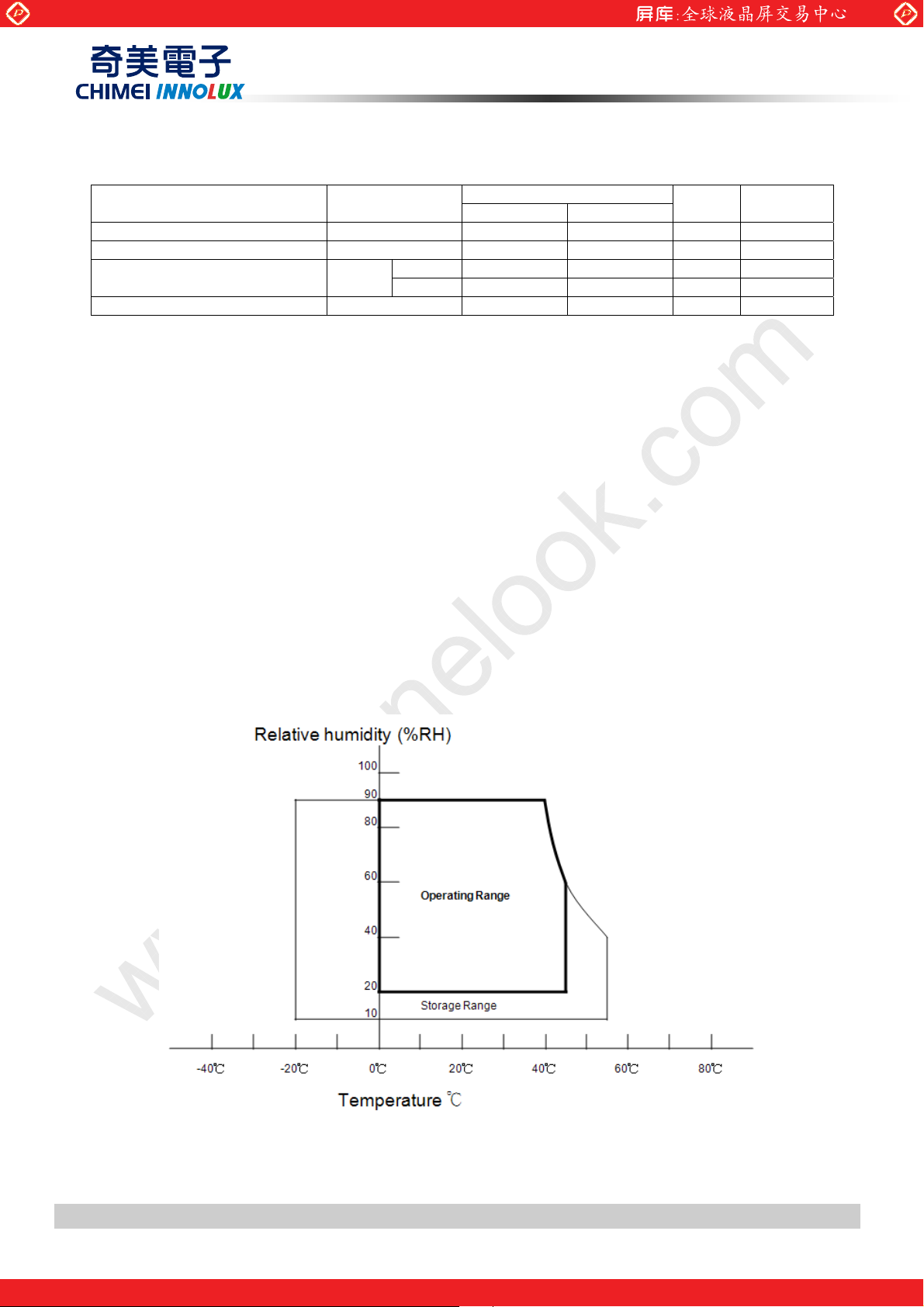
Note (1) Temperature and relative humidity range is shown in the figure below.
(a) 90 %RH Max. (Ta ʀ 40 ºC).
(b) Wet-bulb temperature should be 39 ºC Max. (Ta > 40 ºC).
(c) No condensation.
Note (2) The maximum operating temperature is based on the test condition that the surface temperature of
display area is less than or equal to 65 ºC with LCD module alone in a temperature controlled chamber.
Thermal management should be considered in your product design to prevent the surface temperature of
display area from being over 65 ºC. The range of operating temperature may degrade in case of
improper thermal management in your product design.
Note (3) 11 ms, half sine wave, 1 time for ± X, ± Y, and ± Z.
Note (4) 10 ~ 200 Hz, 10 min, 1 time each X, Y, Z.
Note (5) At testing Vibration and Shock, the fixture in holding the module has to be hard and rigid enough so that
Note
the module would not be twisted or bent by the fixture. The module would not be twisted or bent by the
fixture.
Version 0.0 7 Date烉烉3 Jan 2012
The copyright belongs to CHIMEI InnoLux. Any unauthorized use is prohibited
One step solution for LCD / PDP / OLED panel application: Datasheet, inventory and accessory!
www.panelook.com
Page 8
Global LCD Panel Exchange Center
Symbol
Unit
Room Temperature Image Sticking
RT IS
Invisibility
6% ND (%)
(1)(3)
High
6% ND (%)
(3)
2.2. RATINGS OF IMAGE STICKING
www.panelook.com
PRODUCT SPECIFICATION
Item
Temperature Image Sticking HT IS Invisibility
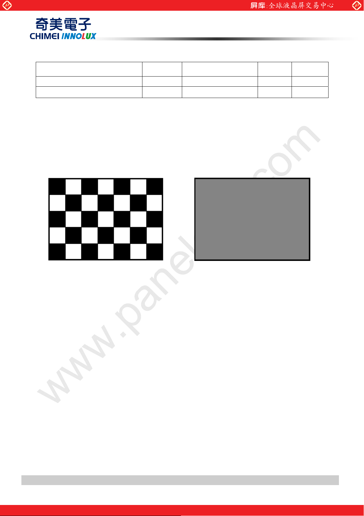
Note (1) Room temperature image sticking test is at 25Ʋ3oC environment and fix the pattern A (checker pattern)
for 12 hours.
Note (2) High temperature image sticking test is at 50Ʋ3
Note (3) Inspection condition is at pattern B (512grade) after 5 mins from pattern A.
A. Pattern A (checker pattern) B. Pattern B (512grade)
o
C environment and fix the pattern A for 12 hours.
Value
Note
(2)
2.3. PACKAGE STORAGE
When storing modules as spares for a long time, the following precaution is necessary.
(a) Do not leave the module in high temperature, and high humidity for a long time, It is highly recommended to
store the module with temperature from 0 to 35 ɗ at normal humidity without condensation.
(b) The module shall be stored in dark place. Do not store the TFT-LCD module in direct sunlight or fluorescent
light.
Version 0.0 8 Date烉烉3 Jan 2012
The copyright belongs to CHIMEI InnoLux. Any unauthorized use is prohibited
One step solution for LCD / PDP / OLED panel application: Datasheet, inventory and accessory!
www.panelook.com
Page 9
Global LCD Panel Exchange Center
Symbol
Unit
Power Supply Voltage
VCC
Logic Input Voltage
Item
Symbol
Value
Min.
Max.
Lamp Voltage
V
W
炼
5000
V
RMS
Power Supply Voltage
VBL030V
(1)
Control Signal Level
炼
-0.37V
(1)
3. ELECTRICAL MAXIMUM RATINGS
3.1. TFT LCD MODULE
Item
VIN -0.3 3.6 V
Note (1) Permanent damage to the device may occur if maximum values are exceeded. Function operation
should be restricted to the conditions described under Normal Operating Conditions.
3.2. BACKLIGHT UNIT
www.panelook.com
PRODUCT SPECIFICATION
Value
Note
Min. Max.
-0.3 13.5 V
(1)
Unit Note
Note (1) Permanent damage to the device may occur if maximum values are exceeded. Function operation
should be restricted to the conditions described under Normal Operating Conditions.
Version 0.0 9 Date烉烉3 Jan 2012
The copyright belongs to CHIMEI InnoLux. Any unauthorized use is prohibited
One step solution for LCD / PDP / OLED panel application: Datasheet, inventory and accessory!
www.panelook.com
Page 10
Global LCD Panel Exchange Center
Parameter
Symbol
Unit
Note
Min.
Typ.
Max.
Power Supply Voltage
VCC
10.81213.2V(1)
Rush Current
IRUSH
3.18
(2)
Power Consumption
White Pattern
PT
炼
11.2
炼
)
Black Pattern
炼
11.1
炼
Horizontal Pattern
炼28炼
Power Supply Current
White Pattern
炼
0.93
炼
)
Black Pattern
炼
0.92
炼
Horizontal Pattern
炼
2.34
炼
LVDS
interface
Differential Input High
Threshold Voltage
VLVTH
+100
mV
)
Differential Input Low
Threshold Voltage
VLVTL
100
mV
Common Input Voltage
VCM
1.0
1.2
1.4
Differential input voltage
(single-end)
|VID|
200炼600
mV
Terminating Resistor
RT炼100炼ohm
CMOS
interface
Input High Threshold Volt
VIH
2.7炼3.3
Input Low Threshold Voltage
VIL
0.7
4. ELECTRICAL CHARACTERISTICS
4.1. TFT LCD MODULE
(Ta = 25 ± 2 ºC)
www.panelook.com
PRODUCT SPECIFICATION
Value
age
炼
炼
炼
炼
炼炼
炼炼
炼
-
A
W(3
A(3
V
V
(4
0
Note (1) The module should be always operated within the above ranges.
Note (2) Measurement condition :
Version 0.0 10 Date烉烉3 Jan 2012
One step solution for LCD / PDP / OLED panel application: Datasheet, inventory and accessory!
The copyright belongs to CHIMEI InnoLux. Any unauthorized use is prohibited
炼
V
www.panelook.com
Page 11
Global LCD Panel Exchange Center
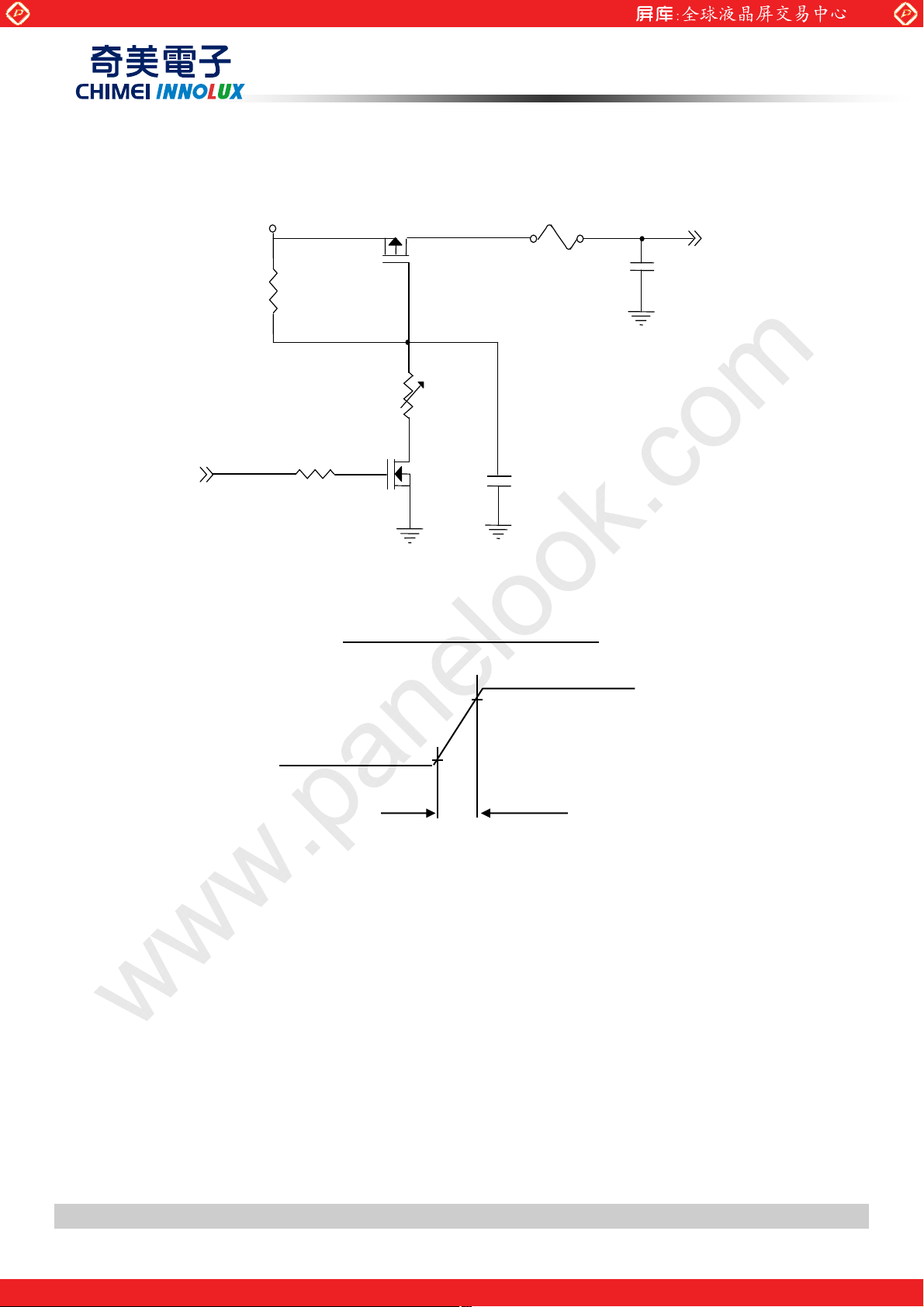
Vcc rising time is at least 470s
470s
GND
0.9Vcc
0.1Vcc
VR1
47K
Q2
2N7002
(Low to High)
(Control Signal)
SW
R2
1K
C1
0.01uF
Vcc1 or
C3
1uF
(LCD Module Input)
FUSE
R1
+5
or
Q1
Si44
1K
+5V or +18V
.0V
www.panelook.com
PRODUCT SPECIFICATION
85DY
Note (3) The specified power supply current is under the conditions at Vcc = 12 V, Ta = 25 ± 2 ºC, fv = 120 Hz,
whereas a power dissipation check pattern below is displayed.
Version 0.0 11 Date烉烉3 Jan 2012
The copyright belongs to CHIMEI InnoLux. Any unauthorized use is prohibited
One step solution for LCD / PDP / OLED panel application: Datasheet, inventory and accessory!
www.panelook.com
Page 12
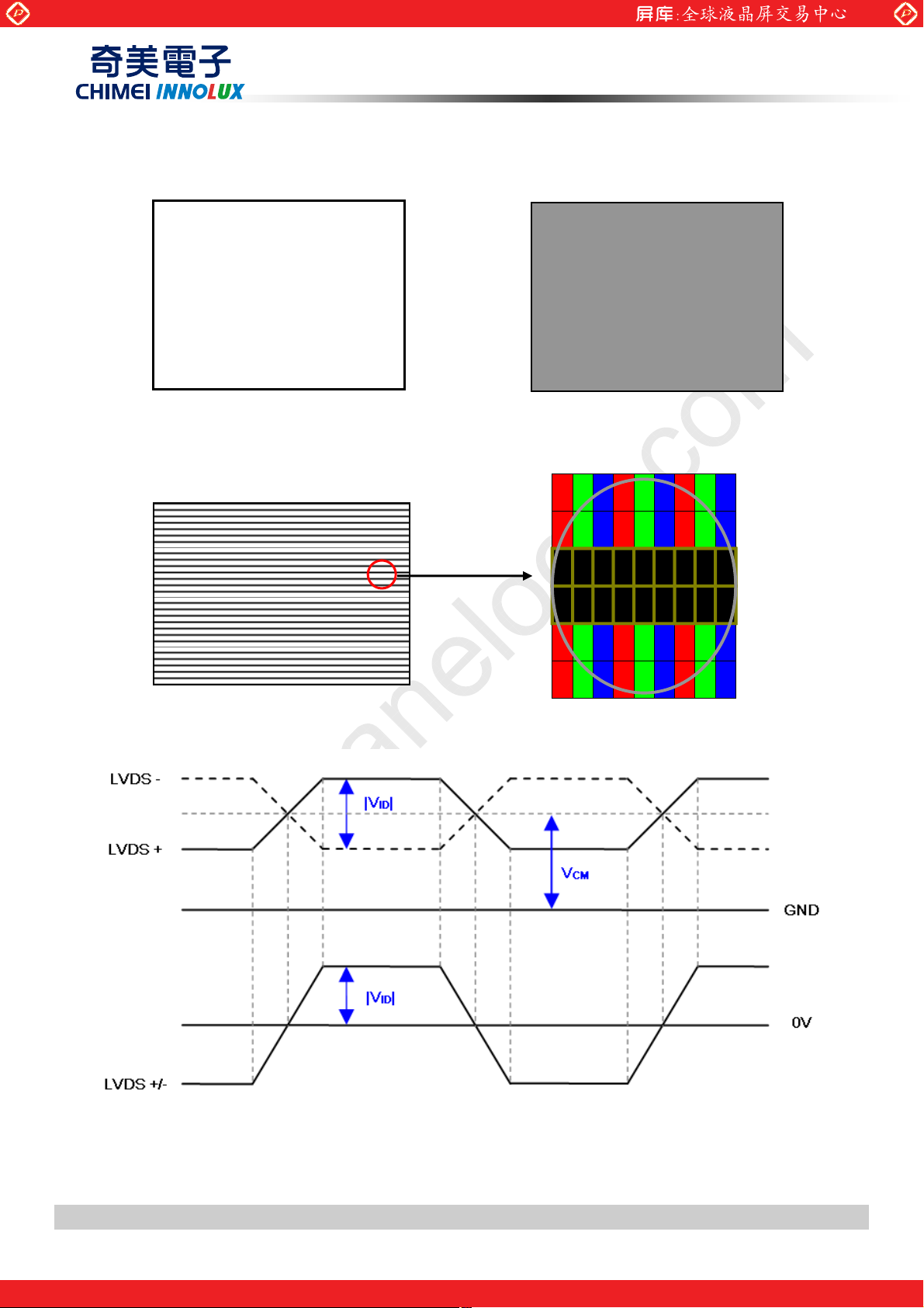
Global LCD Panel Exchange Center
Active Area
b. Black Pattern
a. White Pattern
www.panelook.com
PRODUCT SPECIFICATION
Active Area
Note (4) The LVDS input characteristics are as follows :
RGBRGBRGB
RGBRGBRGBRGBRGBRGB
RGBRGBRGB
RGBRGBRGBRGBRGBRGB
RGBRGBRGB
RGBRGBRGBRGBRGBRGB
RGBRGBRGB
RGBRGBRGBRGBRGBRGB
RGBRGBRGB
RGBRGBRGBRGBRGBRGB
RGBRGBRGB
RGBRGBRGBRGBRGBRGB
Version 0.0 12 Date烉烉3 Jan 2012
The copyright belongs to CHIMEI InnoLux. Any unauthorized use is prohibited
One step solution for LCD / PDP / OLED panel application: Datasheet, inventory and accessory!
www.panelook.com
Page 13

Global LCD Panel Exchange Center
Symbol
Value
Unit
Min.
Typ.
Max.
Power Consumption
PBL-164
180
W
(1),(2) IL = 80 mA
Converter Input Voltage
VBL
22.82425.2
VDC
Converter Input Current
IBL-6.8
7.5
A
Non Dimming
Input Rush current
---
10.6A(3)
Dimming Frequency
FB
150
160
170
Hz
Minimum Duty Ratio
DMIN10-
100%(4)
www.panelook.com
PRODUCT SPECIFICATION
4.2. BACKLIGHT CONVERTER UNIT
4.2.1. CONVERTER CHARACTERISTICS (Ta = 25 ± 2 ºC)
Parameter
Note (1) The power supply capacity should be higher than the total converter power consumption PBL. Since the
pulse width modulation (PWM) mode was applied for backlight dimming, the driving current changed as
PWM duty on and off. The transient response of power supply should be considered for the changing
loading when converter dimming.
Note (2) The measurement condition of Max. value is based on 46" backlight unit under input voltage 24V, average
LED current 80 mA and lighting 1 hour later.
Note (3) The duration of Input Rush Current is about 30ms.
Note (4) 10% minimum duty ratio is only valid for electrical operation.
Note
Version 0.0 13 Date烉烉3 Jan 2012
The copyright belongs to CHIMEI InnoLux. Any unauthorized use is prohibited
One step solution for LCD / PDP / OLED panel application: Datasheet, inventory and accessory!
www.panelook.com
Page 14

Global LCD Panel Exchange Center
Parameter
Symbol
t
Condition
Unit
Min.
Typ.
Max.
On/Off Control Voltage
ON
VBLON
2.0炼5.0
V
OFF炼0炼0.8
V
External PWM Control
Voltage
HI
VEPWM
炼
2.0炼5.0
V
LO炼0炼0.8
V
Error
ERR
Abnormal: Open
Normal: GND
(4)
VBL Rising Time
Tr1炼30
ms
90%VBL
Control Signal Ri
Tr
100
ms
Control Signal Falling Time
Tf
100
ms
PWM Signal Rising Time
TPWMR
50
us
PWM Signal Falling Time
TPWMF
50
us
Input Impedance
Rin炼1
MΩ
PWM Delay Time
TPWM
100
ms
BLON Delay Time
To n
300
炼
ms
To n1
300
ms
BLON Off Time
To ff炼300
炼
ms
www.panelook.com
PRODUCT SPECIFICATION
4.2.2. CONVERTER INTERFACE CHARACTERISTICS
Signal
sing Time
Tes
炼
炼炼炼炼炼
炼炼炼
炼炼炼
炼炼炼
炼炼炼
Value
炼炼
Note1~3
Duty on
Duty off
collector
10%-
炼炼
炼
炼
炼
Note (1) The Dimming signal should be valid before backlight turns on by BLON signal. It is inhibited to change the
external PWM signal during backlight turn on period.
Note (2) The power sequence and control signal timing are shown in the following figure. For a certain reason, the
converter has a possibility to be damaged with wrong power sequence and control signal timing.
Note (3) While system is turned ON or OFF, the power sequences must follow as below descriptions:
Turn ON sequence: VBL → PWM signal → BLON
Turn OFF sequence: BLOFF → PWM signal → VBL
Note (4) When converter protective function is triggered, ERR will output open collector status.
炼炼
炼
炼炼
炼
Version 0.0 14 Date烉烉3 Jan 2012
One step solution for LCD / PDP / OLED panel application: Datasheet, inventory and accessory!
The copyright belongs to CHIMEI InnoLux. Any unauthorized use is prohibited
www.panelook.com
Page 15

Global LCD Panel Exchange Center
Tr1
BL
V
V
V
BLON
EPWM
9
0
%/
2.0V
0
0.8V
0
9
2.0V
0.8V
Ton
T
%/
Backlight on duration
Tr
Ext. Dimming Function
PWMR
T
PWM
www.panelook.com
PRODUCT SPECIFICATION
Ton1
Tf
PWMF
T
Toff
Floating
V
W
External
PWM
Period
External
PWM Duty
100%
Version 0.0 15 Date烉烉3 Jan 2012
The copyright belongs to CHIMEI InnoLux. Any unauthorized use is prohibited
One step solution for LCD / PDP / OLED panel application: Datasheet, inventory and accessory!
www.panelook.com
Page 16

Global LCD Panel Exchange Center
4A/B_SRX0(+/-)
4A/B_SRX1(+/-)
4A/B_SRX2(+/-
)
4A/B_SRX3(+/-)
4A/B_SRX4(+/-)
4A/B_SRCLK(+/-)
4A/B_FRX0(+/-)
4A/B_FRX1(+/-)
4A/B_FRX2(+/-)
4A/B_FRX3(+/-)
4A/B_FRX4(+/-)
4A/B_FRCLK(+/-)
3A/B_SRX0(+/-)
3A/B_SRX1(+/
-)
3A/B_SRX2(+/-
)
3A/B_SRX3(+/-)
3A/B_SRX4(+/-)
3A/B_SRCLK(+/-)
3A/B_FRX0(+/-)
3A/B_FRX1(+/-)
3A/B_FRX2(+/-)
3A/B_FRX3(+/-)
3A/B_FRX4(+/-)
3A/B_FRCLK(+/-)
1A/B_SRX0(+/-)
1A/B_SRX1(+/-)
1A/B_SRX2(+/-
)
1A/B_SRX3(+/-)
1A/B_SRX4(+/-)
1A/B_SRCLK(+/-)
1A/B_FRX0(+/-)
1A/B_FRX1(+/-)
1A/B_FRX2(+/-)
1A/B_FRX3(+/-)
1A/B_FRX4(+/-)
1A/B_FRCLK(+/-)
2A/B_SRX0(+/-)
2A/B_SRX1(+/-)
2A/B_SRX2(+/-
)
2A/B_SRX3(+/-)
2A/B_SRX4(+/-)
2A/B_SRCLK(+/-)
2A/B_FRX0(+/-)
2A/B_FRX1(+/-)
2A/B_FRX2(+/-)
2A/B_FRX3(+/-)
2A/B_FRX4(+/-)
2A/B_FRCLK(+/-)
X(R) Board
X(L) Board
Y Board
Y Board
INPUT
CONNECTOR
HF
JAE Taiwan.
INPUT
CONNECTOR
HF
JAE Taiwan.
INPUT
CONNECTOR
FI-RE51S-HF
JAE Taiwan.
INPUT
CONNECTOR
HF
JAE Taiwan.
CN4
CN3
CN2
CN1
POWER
CONNECTOR
(S20B-PHDS
S-B(LF)(SN))
Vcc
GND
5. BLOCK DIAGRAM
5.1. TFT LCD MODULE
www.panelook.com
PRODUCT SPECIFICATION
OPEN CELL
TFT LCD PANEL
(3840x3x2160)
C Board
FI-RE51S-
One step solution for LCD / PDP / OLED panel application: Datasheet, inventory and accessory!
Version 0.0 16 Date烉烉3 Jan 2012
The copyright belongs to CHIMEI InnoLux. Any unauthorized use is prohibited
FI-RE51S-
FI-RE51S-
www.panelook.com
Page 17

Global LCD Panel Exchange Center
Pin No.
Name
Description
Note
1
GND
Ground.
2
1B_FRX0-
Negative transmission data of First pixel 0.
3
1B_FRX0+
Positive transmission data of First pixel 0.
4
1B_FRX1-
Negative transmission data of First pixel 1.
5
1B_FRX1+
Positive transmission data of First pixel 1.
6
1B_FRX2-
Negative transmission data of First pixel 2.
7
1B_FRX2+
Positive transmission data of First pixel 2.
8
1B_FRCLK-
Negative of First clock.
9
1B_FRCLK+
Positive of First clock.
10
1B_FRX3-
Negative transmission data of First pixel 3.
11
1B_FRX3+
Positive transmission data of First pixel 3.
12
1B_FRX4-
Negative transmission data of First pixel 4.
13
1B_FRX4+
Positive transmission data of First pixel 4.
14
1B_SRX0-
Negative transmission data of Second pixel 0.
15
1B_SRX0+
Positive transmission data of Second pixel 0.
16
1B_SRX1-
Negative transmission data of Second pixel 1.
17
1B_SRX1+
Positive transmission data of Second pixel 1.
18
1B_SRX2-
Negative transmission data of Second pixel 2.
19
1B_SRX2+
Positive transmission data of Second pixel 2.
20
1B_SRCLK-
Negative of Second clock.
21
1B_SRCLK+
Positive of Second clock.
22
1B_SRX3-
Negative transmission data of Second pixel 3.
23
1B_SRX3+
Positive transmission data of Second pixel 3.
24
1B_SRX4-
Negative transmission data of Second pixel 4.
25
1B_SRX4+
Positive transmission data of Second pixel 4.
26
GND
Ground.
27
1A_FRX0-
Negative transmission data of First pixel 0.
28
1A_FRX0+
Positive transmission data of First pixel 0.
29
1A_FRX1-
Negative transmission data of First pixel 1.
30
1A_FRX1+
Positive transmission data of First pixel 1.
31
1A_FRX2-
Negative transmission data of First pixel 2.
32
1A_FRX2+
Positive transmission data of First pixel 2.
33
1A_FRCLK-
Negative of First clock.
34
1A_FRCLK+
Positive of First clock.
35
1A_FRX3-
Negative transmission data of First pixel 3.
36
1A_FRX3+
Positive transmission data of First pixel 3.
37
1A_FRX4-
Negative transmission data of First pixel 4.
38
1A_FRX4+
Positive transmission data of First pixel 4.
39
1A_SRX0-
Negative transmission data of Second pixel 0.
40
1A_SRX0+
Positive transmission data of Second pixel 0.
41
1A_SRX1-
Negative transmission data of Second pixel 1.
42
1A_SRX1+
Positive transmission data of Second pixel 1.
43
1A_SRX2-
Negative transmission data of Second pixel 2.
44
1A_SRX2+
Positive transmission data of Second pixel 2.
45
1A_SRCLK-
Negative of Second clock.
46
1A_SRCLK+
Positive of Second clock.
www.panelook.com
6. LCD INPUT TERMINAL PIN ASSIGNMENT
6.1. TFT LCD MODULE L.V.D.S. INPUT
CN4 Connector Pin Assignment
PRODUCT SPECIFICATION
Version 0.0 17 Date烉烉3 Jan 2012
The copyright belongs to CHIMEI InnoLux. Any unauthorized use is prohibited
One step solution for LCD / PDP / OLED panel application: Datasheet, inventory and accessory!
www.panelook.com
Page 18

Global LCD Panel Exchange Center
47
1A_SRX3-
Negative transmission data of Second pixel 3.
48
1A_SRX3+
Positive transmission data of Second pixel 3.
49
1A_SRX4-
Negative transmission data of Second pixel 4.
50
1A_SRX4+
Positive transmission data of Second pixel 4.
51
GND
Ground.
Pin No.
Name
Description
Note
1
GND
Ground.
2
2B_FRX0-
Negative transmission data of First pixel 0.
3
2B_FRX0+
Positive transmission data of First pixel 0.
4
2B_FRX1-
Negative transmission data of First pixel 1.
5
2B_FRX1+
Positive transmission data of First pixel 1.
6
2B_FRX2-
Negative transmission data of First pixel 2.
7
2B_FRX2+
Positive transmission data of First pixel 2.
8
2B_FRCLK-
Negative of First clock.
9
2B_FRCLK+
Positive of First clock.
10
2B_FRX3-
Negative transmission data of First pixel 3.
11
2B_FRX3+
Positive transmission data of First pixel 3.
12
2B_FRX4-
Negative transmission data of First pixel 4.
13
2B_FRX4+
Positive transmission data of First pixel 4.
14
2B_SRX0-
Negative transmission data of Second pixel 0.
15
2B_SRX0+
Positive transmission data of Second pixel 0.
16
2B_SRX1-
Negative transmission data of Second pixel 1.
17
2B_SRX1+
Positive transmission data of Second pixel 1.
18
2B_SRX2-
Negative transmission data of Second pixel 2.
19
2B_SRX2+
Positive transmission data of Second pixel 2.
20
2B_SRCLK-
Negative of Second clock.
21
2B_SRCLK+
Positive of Second clock.
22
2B_SRX3-
Negative transmission data of Second pixel 3.
23
2B_SRX3+
Positive transmission data of Second pixel 3.
24
2B_SRX4-
Negative transmission data of Second pixel 4.
25
2B_SRX4+
Positive transmission data of Second pixel 4.
26
GND
Ground.
27
2A_FRX0-
Negative transmission data of First pixel 0.
28
2A_FRX0+
Positive transmission data of First pixel 0.
29
2A_FRX1-
Negative transmission data of First pixel 1.
30
2A_FRX1+
Positive transmission data of First pixel 1.
31
2A_FRX2-
Negative transmission data of First pixel 2.
32
2A_FRX2+
Positive transmission data of First pixel 2.
33
2A_FRCLK-
Negative of First clock.
34
2A_FRCLK+
Positive of First clock.
35
2A_FRX3-
Negative transmission data of First pixel 3.
36
2A_FRX3+
Positive transmission data of First pixel 3.
37
2A_FRX4-
Negative transmission data of First pixel 4.
38
2A_FRX4+
Positive transmission data of First pixel 4.
39
2A_SRX0-
Negative transmission data of Second pixel 0.
40
2A_SRX0+
Positive transmission data of Second pixel 0.
41
2A_SRX1-
Negative transmission data of Second pixel 1.
42
2A_SRX1+
Positive transmission data of Second pixel 1.
43
2A_SRX2-
Negative transmission data of Second pixel 2.
CN3 Connector Pin Assignment
www.panelook.com
PRODUCT SPECIFICATION
Version 0.0 18 Date烉烉3 Jan 2012
The copyright belongs to CHIMEI InnoLux. Any unauthorized use is prohibited
One step solution for LCD / PDP / OLED panel application: Datasheet, inventory and accessory!
www.panelook.com
Page 19

Global LCD Panel Exchange Center
44
2A_SRX2+
Positive transmission data of Second pixel 2.
45
2A_SRCLK-
Negative of Second clock.
46
2A_SRCLK+
Positive of Second clock.
47
2A_SRX3-
Negative transmission data of Second pixel 3.
48
2A_SRX3+
Positive transmission data of Second pixel 3.
49
2A_SRX4-
Negative transmission data of Second pixel 4.
50
2A_SRX4+
Positive transmission data of Second pixel 4.
51
GND
Ground.
Pin No.
Name
Description
Note
1
GND
Ground.
2
3B_FRX0-
Negative transmission data of First pixel 0.
3
3B_FRX0+
Positive transmission data of First pixel 0.
4
3B_FRX1-
Negative transmission data of First pixel 1.
5
3B_FRX1+
Positive transmission data of First pixel 1.
6
3B_FRX2-
Negative transmission data of First pixel 2.
7
3B_FRX2+
Positive transmission data of First pixel 2.
8
3B_FRCLK-
Negative of First clock.
9
3B_FRCLK+
Positive of First clock.
10
3B_FRX3-
Negative transmission data of First pixel 3.
11
3B_FRX3+
Positive transmission data of First pixel 3.
12
3B_FRX4-
Negative transmission data of First pixel 4.
13
3B_FRX4+
Positive transmission data of First pixel 4.
14
3B_SRX0-
Negative transmission data of Second pixel 0.
15
3B_SRX0+
Positive transmission data of Second pixel 0.
16
3B_SRX1-
Negative transmission data of Second pixel 1.
17
3B_SRX1+
Positive transmission data of Second pixel 1.
18
3B_SRX2-
Negative transmission data of Second pixel 2.
19
3B_SRX2+
Positive transmission data of Second pixel 2.
20
3B_SRCLK-
Negative of Second clock.
21
3B_SRCLK+
Positive of Second clock.
22
3B_SRX3-
Negative transmission data of Second pixel 3.
23
3B_SRX3+
Positive transmission data of Second pixel 3.
24
3B_SRX4-
Negative transmission data of Second pixel 4.
25
3B_SRX4+
Positive transmission data of Second pixel 4.
26
GND
Ground.
27
3A_FRX0-
Negative transmission data of First pixel 0.
28
3A_FRX0+
Positive transmission data of First pixel 0.
29
3A_FRX1-
Negative transmission data of First pixel 1.
30
3A_FRX1+
Positive transmission data of First pixel 1.
31
3A_FRX2-
Negative transmission data of First pixel 2.
32
3A_FRX2+
Positive transmission data of First pixel 2.
33
3A_FRCLK-
Negative of First clock.
34
3A_FRCLK+
Positive of First clock.
35
3A_FRX3-
Negative transmission data of First pixel 3.
36
3A_FRX3+
Positive transmission data of First pixel 3.
37
3A_FRX4-
Negative transmission data of First pixel 4.
38
3A_FRX4+
Positive transmission data of First pixel 4.
39
3A_SRX0-
Negative transmission data of Second pixel 0.
40
3A_SRX0+
Positive transmission data of Second pixel 0.
CN2 Connector Pin Assignment
www.panelook.com
PRODUCT SPECIFICATION
Version 0.0 19 Date烉烉3 Jan 2012
The copyright belongs to CHIMEI InnoLux. Any unauthorized use is prohibited
One step solution for LCD / PDP / OLED panel application: Datasheet, inventory and accessory!
www.panelook.com
Page 20

Global LCD Panel Exchange Center
41
3A_SRX1-
Negative transmission data of Second pixel 1.
42
3A_SRX1+
Positive transmission data of Second pixel 1.
43
3A_SRX2-
Negative transmission data of Second pixel 2.
44
3A_SRX2+
Positive transmission data of Second pixel 2.
45
3A_SRCLK-
Negative of Second clock.
46
3A_SRCLK+
Positive of Second clock.
47
3A_SRX3-
Negative transmission data of Second pixel 3.
48
3A_SRX3+
Positive transmission data of Second pixel 3.
49
3A_SRX4-
Negative transmission data of Second pixel 4.
50
3A_SRX4+
Positive transmission data of Second pixel 4.
51
GND
Ground.
Pin No.
Name
Description
Note
1
GND
Ground.
2
4B_FRX0-
Negative transmission data of First pixel 0.
3
4B_FRX0+
Positive transmission data of First pixel 0.
4
4B_FRX1-
Negative transmission data of First pixel 1.
5
4B_FRX1+
Positive transmission data of First pixel 1.
6
4B_FRX2-
Negative transmission data of First pixel 2.
7
4B_FRX2+
Positive transmission data of First pixel 2.
8
4B_FRCLK-
Negative of First clock.
9
4B_FRCLK+
Positive of First clock.
10
4B_FRX3-
Negative transmission data of First pixel 3.
11
4B_FRX3+
Positive transmission data of First pixel 3.
12
4B_FRX4-
Negative transmission data of First pixel 4.
13
4B_FRX4+
Positive transmission data of First pixel 4.
14
4B_SRX0-
Negative transmission data of Second pixel 0.
15
4B_SRX0+
Positive transmission data of Second pixel 0.
16
4B_SRX1-
Negative transmission data of Second pixel 1.
17
4B_SRX1+
Positive transmission data of Second pixel 1.
18
4B_SRX2-
Negative transmission data of Second pixel 2.
19
4B_SRX2+
Positive transmission data of Second pixel 2.
20
4B_SRCLK-
Negative of Second clock.
21
4B_SRCLK+
Positive of Second clock.
22
4B_SRX3-
Negative transmission data of Second pixel 3.
23
4B_SRX3+
Positive transmission data of Second pixel 3.
24
4B_SRX4-
Negative transmission data of Second pixel 4.
25
4B_SRX4+
Positive transmission data of Second pixel 4.
26
GND
Ground.
27
4A_FRX0-
Negative transmission data of First pixel 0.
28
4A_FRX0+
Positive transmission data of First pixel 0.
29
4A_FRX1-
Negative transmission data of First pixel 1.
30
4A_FRX1+
Positive transmission data of First pixel 1.
31
4A_FRX2-
Negative transmission data of First pixel 2.
32
4A_FRX2+
Positive transmission data of First pixel 2.
33
4A_FRCLK-
Negative of First clock.
34
4A_FRCLK+
Positive of First clock.
35
4A_FRX3-
Negative transmission data of First pixel 3.
36
4A_FRX3+
Positive transmission data of First pixel 3.
37
4A_FRX4-
Negative transmission data of First pixel 4.
CN1 Connector Pin Assignment
www.panelook.com
PRODUCT SPECIFICATION
Version 0.0 20 Date烉烉3 Jan 2012
The copyright belongs to CHIMEI InnoLux. Any unauthorized use is prohibited
One step solution for LCD / PDP / OLED panel application: Datasheet, inventory and accessory!
www.panelook.com
Page 21

Global LCD Panel Exchange Center
38
4A_FRX4+
Positive transmission data of First pixel 4.
39
4A_SRX0-
Negative transmission data of Second pixel 0.
40
4A_SRX0+
Positive transmission data of Second pixel 0.
41
4A_SRX1-
Negative transmission data of Second pixel 1.
42
4A_SRX1+
Positive transmission data of Second pixel 1.
43
4A_SRX2-
Negative transmission data of Second pixel 2.
44
4A_SRX2+
Positive transmission data of Second pixel 2.
45
4A_SRCLK-
Negative of Second clock.
46
4A_SRCLK+
Positive of Second clock.
47
4A_SRX3-
Negative transmission data of Second pixel 3.
48
4A_SRX3+
Positive transmission data of Second pixel 3.
49
4A_SRX4-
Negative transmission data of Second pixel 4.
50
4A_SRX4+
Positive transmission data of Second pixel 4.
51
GND
Ground.
Port
CH of LVDS
Data Stream
1st Port
First pixel
1, 5, 9, ..........., 1913, 1917
2nd Port
Second pixel
2, 6, 10, ........., 1914, 1918
3rd Port
Third pixel
3, 7, 11, ........., 1915, 1919
4th Port
Fourth pixel
4, 8, 12, ........., 1916, 1920
Note (1) CN4ˣCN3ˣCN2ˣCN1 connector part no.: FI-RE51S-HF,JAE Taiwan.
www.panelook.com
PRODUCT SPECIFICATION
Note (2) LVDS 4-Port Data Mapping
Version 0.0 21 Date烉烉3 Jan 2012
The copyright belongs to CHIMEI InnoLux. Any unauthorized use is prohibited
One step solution for LCD / PDP / OLED panel application: Datasheet, inventory and accessory!
www.panelook.com
Page 22

Global LCD Panel Exchange Center
Pin No.
Symbol
Description
Note
1
NC
Not connection
(2)
2
NC
Not connection
(2)
3
VCC
+12.0V power supply
4
VCC
+12.0V power supply
5
VCC
+12.0V power supply
6
NC
Not connection
(2)
7
VCC
+12.0V power supply
8
NC
Not connection
(2)
9
VCC
+12.0V power supply
10
NC
Not connection
(2)
11
GND
Ground12NC
Not connection
(2)
13
GND
Ground14NC
Not connection
(2)
15
NC
Not connection
(2)
16
NC
Not connection
(2)
17
NC
Not connection
(2)
18
GND
Ground19GND
Ground20GND
Ground
6.2. TFT LCD MODULE POWER INPUT
CN9 Connector Pin Assignment
www.panelook.com
PRODUCT SPECIFICATION
Note (1) CN9 connector part no.: S20B-PHDSS-B(LF)(SN), JST(㖍㛔⡻叿䪗⫸),⽟忂䪗⫸ or equivalent.
Note (2) Reserved for internal use. Please leave it open.
Version 0.0 22 Date烉烉3 Jan 2012
The copyright belongs to CHIMEI InnoLux. Any unauthorized use is prohibited
One step solution for LCD / PDP / OLED panel application: Datasheet, inventory and accessory!
www.panelook.com
Page 23

Global LCD Panel Exchange Center
Pin №
Signal name
1
+24 V
2
3
4
5
6
7
8
9
10
11
Normal (GND)
Abnormal (Open collector)
12
BLON
BL ON/OFF
13
NC
NC
14
Pin №
Symbol
Feature
1
VLED+
2
VLED+
3
456
7
N1
8
N2
9N310
N4
www.panelook.com
PRODUCT SPECIFICATION
6.3. CONVERTER UNIT
CN1: CI0114M1HR0-LF (CvilLux) or S14B-PH-SM4-TB(LF)(SN) (JST)
V
BL
GND GND
Feature
ERR
E_PWM External PWM Control
CN2- CN3: 51281-1094 (Molex) or 7083K-F10N-00L (E&T)
Positive of LED String
NC NC
Negative of LED String
Version 0.0 23 Date烉烉3 Jan 2012
One step solution for LCD / PDP / OLED panel application: Datasheet, inventory and accessory!
The copyright belongs to CHIMEI InnoLux. Any unauthorized use is prohibited
www.panelook.com
Page 24

Global LCD Panel Exchange Center
6.4. BLOCK DIAGRAM OF IMAGE SIGNAL
The video picture (3840x2160) should be divided into four parts: each one is 960x2160 resolution. Signals of these
four parts should be delivered into the module individually through each 4-channel LVDS interface. But it must be
“synchronous” mutually between signals from these four 4-channel LVDS interfaces. And the protocol is specified
in the LVDS interface specification.
www.panelook.com
PRODUCT SPECIFICATION
6.5. BLOCK DIAGRAM OF L.V.D.S.
Version 0.0 24 Date烉烉3 Jan 2012
The copyright belongs to CHIMEI InnoLux. Any unauthorized use is prohibited
One step solution for LCD / PDP / OLED panel application: Datasheet, inventory and accessory!
www.panelook.com
Page 25

Global LCD Panel Exchange Center
LVDS interface receiver required input data mapping table
LVDS Channel E0
LVDS output
TA6
TA5
TA4
TA3
TA2
TA1
TA0
Data order
FG0
FR5
FR4
FR3
FR2
FR1
FR0
LVDS Channel E1
LVDS output
TB6
TB5
TB4
TB3
TB2
TB1
TB0
Data order
FB1
FB0
FG5
FG4
FG3
FG2
FG1
LVDS Channel E2
LVDS output
TC6
TC5
TC4
TC3
TC2
TC1
TC0
Data order
DENANA
FB5
FB4
FB3
FB2
LVDS Channel E3
LVDS output
TD6
TD5
TD4
TD3
TD2
TD1
TD0
Data order
NA
FB7
FB6
FG7
FG6
FR7
FR6
LVDS Channel E4
LVDS output
TE6
TE5
TE4
TE3
TE2
TE1
TE0
Data order
NA
FB9
FB8
FG9
FG8
FR9
FR8
LVDS Channel O0
LVDS output
TA6
TA5
TA4
TA3
TA2
TA1
TA0
Data order
SG0
SR5
SR4
SR3
SR2
SR1
SR0
LVDS Channel O1
LVDS output
TB6
TB5
TB4
TB3
TB2
TB1
TB0
Data order
SB1
SB0
SG5
SG4
SG3
SG2
SG1
LVDS Channel O2
LVDS output
TC6
TC5
TC4
TC3
TC2
TC1
TC0
Data order
DENANA
SB5
SB4
SB3
SB2
LVDS Channel O3
LVDS output
TD6
TD5
TD4
TD3
TD2
TD1
TD0
Data order
NA
SB7
SB6
SG7
SG6
SR7
SR6
LVDS Channel O4
LVDS output
TE6
TE5
TE4
TE3
TE2
TE1
TE0
Data order
NA
SB9
SB8
SG9
SG8
SR9
SR8
6.6. L.V.D.S. INTERFACE
www.panelook.com
PRODUCT SPECIFICATION
R0~R9 : Pixel R Data (9; MSB, 0; LSB)
G0~G9 : Pixel G Data (9; MSB, 0; LSB)
B0~B9 : Pixel B Data (9; MSB, 0; LSB)
DE : Data enable signal
Version 0.0 25 Date烉烉3 Jan 2012
The copyright belongs to CHIMEI InnoLux. Any unauthorized use is prohibited
One step solution for LCD / PDP / OLED panel application: Datasheet, inventory and accessory!
www.panelook.com
Page 26

Global LCD Panel Exchange Center
Data Signal
Red
Green
Blue
R9R8R7R6R5R4R3R2R1R0G9G8G7G6G5G4G3G2G1G0B9B8B7B6B5B4B3B2B1
B0
Basic
Colors
Black
Red
Green
Blue
Cyan
Magenta
Yellow
White
0
1
0
0
0
1
1
1
0
1
0
0
0
1
1
1
0
1
0
0
0
1
1
1
0
1
0
0
0
1
1
1
0
1
0
0
0
1
1
1
0
1
0
0
0
1
1
1
0
1
0
0
0
1
1
1
0
1
0
0
0
1
1
1
0
1
0
0
0
1
1
1
0
1
0
0
0
1
1
1
0
0
1
0
1
0
1
1
0
0
1
0
1
0
1
1
0
0
1
0
1
0
1
1
0
0
1
0
1
0
1
1
0
0
1
0
1
0
1
1
0
0
1
0
1
0
1
1
0
0
1
0
1
0
1
1
0
0
1
0
1
0
1
1
0
0
1
0
1
0
1
1
0
0
1
0
1
0
1
1
0
0
0
1
1
1
0
1
0
0
0
1
1
1
0
1
0
0
0
1
1
1
0
1
0
0
0
1
1
1
0
1
0
0
0
1
1
1
0
1
0
0
0
1
1
1
0
1
0
0
0
1
1
1
0
1
0
0
0
1
1
1
0
1
0
0
0
1
1
1
0
1
0
0
0
1
1
1
0
1
Gray
Scale
Of
Red
Red (0) / Dark
Red (1)
Red (2)
:
:
Red (1021)
Red (1022)
Red (1023)
0
0
0
1
1
1
0
0
0
1
1
1
0
0
0
:
:
1
1
1
0
0
0
:
:
1
1
1
0
0
0
:
:
1
1
1
0
0
0
:
:
1
1
1
0
0
0
:
:
1
1
1
0
0
0
:
:
1
1
1
0
0
1
:
:
0
1
1
0
1
0
:
:
1
0
1
0
0
0
:
:
0
0
0
0
0
0
:
:
0
0
0
0
0
0
:
:
0
0
0
0
0
0
:
:
0
0
0
0
0
0
:
:
0
0
0
0
0
0
:
:
0
0
0
0
0
0
:
:
0
0
0
0
0
0
:
:
0
0
0
0
0
0
:
:
0
0
0
0
0
0
:
:
0
0
0
0
0
0
:
;
0
0
0
0
0
0
:
:
0
0
0
0
0
0
:
:
0
0
0
0
0
0
:
:
0
0
0
0
0
0
:
:
0
0
0
0
0
0
:
:
0
0
0
0
0
0
:
:
0
0
0
0
0
0
:
:
0
0
0
0
0
0
:
:
0
0
0
0
0
0
:
:
0
0
0
Gray
Scale
Of
Green
Green (0) / Dark
Green (1)
Green (2)
Green (1021)
Green (1022)
Green (1023)
0
0
0
:
:
0
0
0
0
0
0
:
:
0
0
0
0
0
0
:
:
0
0
0
0
0
0
:
:
0
0
0
0
0
0
:
:
0
0
0
0
0
0
:
:
0
0
0
0
0
0
:
:
0
0
0
0
0
0
:
:
0
0
0
0
0
0
:
:
0
0
0
0
0
0
:
:
0
0
0
0
0
0
:
:
1
1
1
0
0
0
:
:
1
1
1
0
0
0
:
:
1
1
1
0
0
0
:
:
1
1
1
0
0
0
:
:
1
1
1
0
0
0
:
:
1
1
1
0
0
0
:
:
1
1
1
0
0
0
:
:
1
1
1
0
0
1
:
:
0
1
1
0
1
0
:
:
1
0
1
0
0
0
:
:
0
0
0
0
0
0
:
:
0
0
0
0
0
0
:
:
0
0
0
0
0
0
:
:
0
0
0
0
0
0
:
:
0
0
0
0
0
0
:
:
0
0
0
0
0
0
:
:
0
0
0
0
0
0
:
:
0
0
0
0
0
0
:
:
0
0
0
0
0
0
:
:
0
0
0
Gray
Scale
Of
Blue
Blue (0) / Dark
Blue (1)
Blue (2)
Blue (1021)
Blue (1022)
Blue (1023)
0
0
0
:
:
0
0
0
0
0
0
:
:
0
0
0
0
0
0
:
:
0
0
0
0
0
0
:
:
0
0
0
0
0
0
:
:
0
0
0
0
0
0
:
:
0
0
0
0
0
0
:
:
0
0
0
0
0
0
:
:
0
0
0
0
0
0
:
:
0
0
0
0
0
0
:
:
0
0
0
0
0
0
:
:
0
0
0
0
0
0
:
:
0
0
0
0
0
0
:
:
0
0
0
0
0
0
:
:
0
0
0
0
0
0
:
:
0
0
0
0
0
0
:
:
0
0
0
0
0
0
:
:
0
0
0
0
0
0
:
:
0
0
0
0
0
0
:
:
0
0
0
0
0
0
:
:
0
0
0
0
0
0
:
:
1
1
1
0
0
0
:
:
1
1
1
0
0
0
:
:
1
1
1
0
0
0
:
:
1
1
1
0
0
0
:
:
1
1
1
0
0
0
:
:
1
1
1
0
0
0
:
:
1
1
1
0
0
0
:
:
1
1
1
0
0
1
:
:
0
1
1
0
1
0
:
:
1
0
1
6.7. COLOR DATA INPUT ASSIGNMENT
The brightness of each primary color (red, green and blue) is based on the 10-bit gray scale data input for the color.
The higher the binary input the brighter the color. The table below provides the assignment of color versus data
input.
Color
www.panelook.com
PRODUCT SPECIFICATION
:
:
:
:
Note (1) 0: Low Level Voltage, 1: High Level Voltage
Version 0.0 26 Date烉烉3 Jan 2012
One step solution for LCD / PDP / OLED panel application: Datasheet, inventory and accessory!
The copyright belongs to CHIMEI InnoLux. Any unauthorized use is prohibited
www.panelook.com
Page 27

Global LCD Panel Exchange Center
T
Tvb
T
Th
Signal
Item
Symbol
Min.
Typ.
Max.
Unit
Note
Frequency
1/Tc
50
74.25
80
MHZ
(1)(5)
Input cycle to
cycle jitter
Trcl
200
ps
Spread
spectrum
clkin_mod
F
2%
F
+2%
MHz
(4)
Spread
spectrum
KHz
LVDS Receiver Data
Receiver
Skew Margin
ps
Vertical Active
(4-
Active Area)
Frame Rate
Fr炼120
Hz
Hz
To ta l
Tv
2168
炼
3160
Th
Tv=Tvd+Tvb
Display
Tvd
炼
2160炼Th
Blank
Tvb
8炼1000
Th
Horizontal Active Display Term
(4-CH LVDS,960X2160 Active Area)
To ta l
Th
1100
炼
1800
Tc
Th=Thd+Thb
Display
Thd
炼
960炼Tc
Blank
Thb
140
420
840
Tc
DE
Thb
Valid display data (
Tc
DCLK
Thd
DE
DATA
焍焍焍
焍
www.panelook.com
PRODUCT SPECIFICATION
7. TIMING REQUIREMENTS OF IMAGE SIGNAL
7.1. INPUT SIGNAL TIMING SPECIFICATIONS
The input signal timing specifications are shown as the following table and timing diagram.
LVDS
Receiver
Clock
Display Term
CH LVDS,960X2160
Note (1) Please make sure the range of pixel clock has follow the below equation烉
Fclkin(max) ʁ Fr ʹ Tv ʹ Th
Fr ʹ Tv ʹ Th ʁ Fclkin (min)
INPUT SIGNAL TIMING DIAGRAM
F
F
SSM
T
RSKM
炼炼
-
clkin
炼 炼
-400
炼
炼
clkin
200
400
炼
(3)
v
vd
240 DCLK)
Version 0.0 27 Date烉烉3 Jan 2012
One step solution for LCD / PDP / OLED panel application: Datasheet, inventory and accessory!
The copyright belongs to CHIMEI InnoLux. Any unauthorized use is prohibited
www.panelook.com
Page 28

Global LCD Panel Exchange Center
RXCLK+/-
RXn+/-
T
www.panelook.com
PRODUCT SPECIFICATION
Note (2) The input clock cycle-to-cycle jitter is defined as below figures. Trcl =ɴT1 – Tɴ
Note (3) The SSCG (Spread spectrum clock generator) is defined as below figures.
TcTc
Note (4) LVDS receiver skew margin is defined and shown as below.
LVDS RECEIVER INTERFACE TIMING DIAGRAM
Tc
RSKM
Version 0.0 28 Date烉烉3 Jan 2012
The copyright belongs to CHIMEI InnoLux. Any unauthorized use is prohibited
One step solution for LCD / PDP / OLED panel application: Datasheet, inventory and accessory!
www.panelook.com
Page 29

Global LCD Panel Exchange Center
0.5ʀT1ʀ10ms
500ms ʀT4
5
0V
0V
5
T6T
T3T
0.1V
0.1VCC
T4T
Power On
Backlight (Recommended)
100msʀT6
T
T
Option Signals (SELLVDS)
0ʀT7ʀT2
Power Off
7.2. POWER ON/OFF SEQUENCE
To prevent a latch-up or DC operation of LCD module, the power on/off sequence should be as the diagram below.
www.panelook.com
PRODUCT SPECIFICATION
0ʀT2ʀ50ms
0ʀT3ʀ50ms
LVDS Signals
0ʀT8ʀT3
500msʀT5
cc
1
2
7
0%
0%
8
5
Note (1) The supply voltage of the external system for the module input should follow the definition of Vcc.
Note (2) Apply the voltage within the LCD operation range. When the backlight turns on before the LCD operation
or the LCD turns off before the backlight turns off, the display may momentarily become abnormal
screen.
Note (3) In case of VCC is in off level, please keep the level of input signals on the low or high impedance. If T2<0,
that maybe cause electrical overstress failures.
Note (4) T4 should be measured after the module has been fully discharged between power off and on period.
Note (5) Interface signal shall not be kept at high impedance when the power is on.
Version 0.0 29 Date烉烉3 Jan 2012
One step solution for LCD / PDP / OLED panel application: Datasheet, inventory and accessory!
The copyright belongs to CHIMEI InnoLux. Any unauthorized use is prohibited
www.panelook.com
Page 30

Global LCD Panel Exchange Center
Item
Symbol
Value
Unit
Ambient Temperature
Ta
252
o
C
Ambient Humidity
Ha
5010
%RH
Supply Voltage
VCC5.0
V
Input Signal
According to typical value in "3. ELECTRICAL CHARACTERISTICS"
Frame Rate
Fr60
Hz
Item
Symbol
Condition
Min.
Typ.
Max.
Unit
Note
Contrast Ratio
CR
at
800
1000
-
Note (2)
Response Time
Gray to
gray
6.512ms
Note (3)
Center Luminance of White
LC400
450
cd/m
2
Note (4)
White Variation
W
1.6
-
Note (7)
Cross Talk
CT2%
Note (5)
Color
Chromaticity
Rx
Typ.
-0.03
0.663
Typ.
+0.03
-
Note (6)
Ry
0.330
-
Gx
0.184
-
Gy
0.691
-
Bx
0.149
-
By
0.043
-
Wx
0.280
-
Wy
0.290
-
Color Gamut
C.G-72%NTSC
Viewing
Angle
Horizontal
x+
CR30
80
88
Deg.
Note (1)
x-
80
88
Vertical
Y+
80
88
Y-
80
88
8. OPTICAL CHARACTERISTICS <TBD>
8.1. TEST CONDITIONS
8.2. OPTICAL SPECIFICATIONS
The relative measurement methods of optical characteristics are shown in 8.2 Notes. The following items should
be measured under the test conditions described in 8.1 and stable environment shown in Note (6).
www.panelook.com
PRODUCT SPECIFICATION
Red
Green
Blue
White
x=0, Y=0
Viewing angle
normal direction
Version 0.0 30 Date烉烉3 Jan 2012
One step solution for LCD / PDP / OLED panel application: Datasheet, inventory and accessory!
The copyright belongs to CHIMEI InnoLux. Any unauthorized use is prohibited
www.panelook.com
Page 31

Global LCD Panel Exchange Center
12 o’clock direction
6 o’clock
x
x
x
y+
y-x+
= 90º
= 90º
Time
100%
90%
10%
0%
Gray to gray
switching time
Time
Gray to gray
switching time
Note (1) Definition of Viewing Angle (x, y):
Viewing angles are measured by Autronic Conoscope Cono-80
www.panelook.com
PRODUCT SPECIFICATION
Normal
x = y = 0º
y- y
X-
y- = 90º
Note (2) Definition of Contrast Ratio (CR):
The contrast ratio can be calculated by the following expression.
Contrast Ratio (CR) = L1023 / L0
L1023: Luminance of gray level 1023
L 0: Luminance of gray level 0
CR = CR (7), where CR (X) is corresponding to the Contrast Ratio of the point X at the figure in Note (7).
Note (3) Definition of Gray to Gray Switching Time:
-
y+ = 90º
X+
Optical
Response
The driving signal means the signal of gray level 0, 124, 252, 380, 508, 636, 764, 892, and 1023.Gray to
gray. Average time means the average switching time of gray level 0, 124, 252, 380, 508, 636, 764, 892,
and 1023 to each other.
Version 0.0 31 Date烉烉3 Jan 2012
One step solution for LCD / PDP / OLED panel application: Datasheet, inventory and accessory!
The copyright belongs to CHIMEI InnoLux. Any unauthorized use is prohibited
www.panelook.com
Page 32

Global LCD Panel Exchange Center
Active Area
Y
(D/2,W/8)
Y
(7D/8,W/2)
Y
Y
(D/8,W/2)
(0, 0)
(D,W)
Gray 512
Active Area
(D/4,W/4)
(3D/4,3W/4)
(0, 0)
Y
(D/2,W/8)
Y
(D/2,7W/8)
(D, W)
Gray 512
Gray 1023
Y
(7D/8,W/2)
Y
B, L
(D/8,W/2)
Note (4) Definition of Luminance of White (Lc):
Measure the luminance of gray level 1023 at center point
www.panelook.com
PRODUCT SPECIFICATION
L
= L (7)
C
Where L (x) is corresponding to the luminance of the point X at the figure in Note (7).
Note (5) Definition of Cross Talk (CT):
CT = | Y
– YA | / YA 100 (%)
B
Where:
Y
Y
A, L
(D/2,7W/8)
A, D
= Luminance of measured location without gray level 1023 pattern (cd/m2)
A
= Luminance of measured location with gray level 1023 pattern (cd/m2)
B
A, U
A, R
B, D
B, U
B, R
Version 0.0 32 Date烉烉3 Jan 2012
The copyright belongs to CHIMEI InnoLux. Any unauthorized use is prohibited
One step solution for LCD / PDP / OLED panel application: Datasheet, inventory and accessory!
www.panelook.com
Page 33

Global LCD Panel Exchange Center
D
W
Active
:
oint
X=1 to 13
5
4
3D/10
5D/10
7D/10
W/10
5W/10
7W/10
X
1
2
3
10
9678111213
9W/10
3W/10
D/10
9D/10
Note (6) Measurement Setup:
The LCD module should be stabilized at given temperature for 1 hour to avoid abrupt temperature
change during measuring. In order to stabilize the luminance, the measurement should be executed after
lighting backlight for 1 hour in a windless room.
www.panelook.com
PRODUCT SPECIFICATION
Note (7) Definition of White Variation (W):
Measure the luminance of gray level 512 at 13 points
W = Maximum [L (1), L (2), L (3), L (4),ˣˣˣ, L (13)] / Minimum [L (1), L (2), L (3), L (4),ˣˣˣ, L (13)]
Vertical Line
Area
Test P
Version 0.0 33 Date烉烉3 Jan 2012
The copyright belongs to CHIMEI InnoLux. Any unauthorized use is prohibited
One step solution for LCD / PDP / OLED panel application: Datasheet, inventory and accessory!
www.panelook.com
Page 34

Global LCD Panel Exchange Center
www.panelook.com
9. PRECAUTIONS <TBD>
9.1. ASSEMBLY AND HANDLING PRECAUTIONS
(1) Do not apply rough force such as bending or twisting to the module during assembly.
(2) It is recommended to assemble or to install a module into the user’s system in clean working areas. The dust
and oil may cause electrical short or worsen the polarizer.
(3) Do not apply pressure or impulse to the module to prevent the damage of LCD panel and Backlight.
(4) Always follow the correct power-on sequence when the LCD module is turned on. This can prevent the
damage and latch-up of the CMOS LSI chips.
(5) Bezel of Set can not press or touch the panel surface. It will make light leakage or scrape.
(6) Do not plug in or pull out the I/F connector while the module is in operation.
(7) Do not disassemble the module.
(8) Use a soft dry cloth without chemicals for cleaning, because the surface of polarizer is very soft and easily
PRODUCT SPECIFICATION
scratched.
(9) Moisture can easily penetrate into LCD module and may cause the damage during operation.
(10) When storing modules as spares for a long time, the following precaution is necessary.
a. Do not leave the module in high temperature, and high humidity for a long time.It is highly
recommended to store the module with temperature from 0 to 35 ºC at normal humidity without
condensation.
b. The module shall be stored in dark place. Do not store the TFT-LCD module in direct sunlight or
fluorescent light.
(11) When ambient temperature is lower than 10 ºC, the display quality might be reduced. For example, the
response time will become slow, and the starting voltage of CCFL will be higher than that of room temperature.
9.2. SAFETY PRECAUTIONS
(1) The startup voltage of a Backlight is approximately 1000 Volts. It may cause an electrical shock while
assembling with the inverter. Do not disassemble the module or insert anything into the Backlight unit.
(2) If the liquid crystal material leaks from the panel, it should be kept away from the eyes or mouth. In case of
contact with hands, skin or clothes, it has to be washed away thoroughly with soap.
(3) After the module’s end of life, it is not harmful in case of normal operation and storage.
9.3. SAFETY STANDARDS
The LCD module should be certified with safety regulations as follows:
(1) UL60950-1 or updated standard.
(2) IEC60950-1 or updated standard.
(3) UL60065 or updated standard.
(4) IEC60065 or updated standard.
Version 0.0 34 Date烉烉3 Jan 2012
The copyright belongs to CHIMEI InnoLux. Any unauthorized use is prohibited
One step solution for LCD / PDP / OLED panel application: Datasheet, inventory and accessory!
www.panelook.com
Page 35

Global LCD Panel Exchange Center
Product Line
Year, Month, Date
CMI Internal Use
CMI Internal Use
Revision
CMI Internal Use
Serial No.
X X X X X X X Y M D L N N N N
RoHS
GEMN
10. DEFINITION OF LABELS
10.1. CMI MODULE LABEL
The barcode nameplate is pasted on each module as illustration, and its definitions are as following explanation.
Model Name: V460DC1-LD1
Revision: Rev. XX, for example: A0, A1… B1, B2… or C1, C2…etc.
www.panelook.com
PRODUCT SPECIFICATION
V460DC1 –LD1 Rev. XX
E207943
MADE IN TAIWAN
Serial ID: X X X X X X X Y M D L N N N N
Serial ID includes the information as below:
Manufactured Date:
Year : 2001=1, 2002=2, 2003=3, 2004=4…2010=0, 2011=1, 2012=2…
Month: 1~9, A~C, for Jan. ~ Dec.
Day: 1~9, A~Y, for 1st to 31st, exclude I ,O, and U.
Revision Code : Cover all the change
Serial No. : Manufacturing sequence of product
Product Line : 1 → Line1, 2 → Line 2, …etc.
Version 0.0 35 Date烉烉3 Jan 2012
The copyright belongs to CHIMEI InnoLux. Any unauthorized use is prohibited
One step solution for LCD / PDP / OLED panel application: Datasheet, inventory and accessory!
www.panelook.com
Page 36

Global LCD Panel Exchange Center
10.2. WARRANTY LABEL <TBD>
Warranty labels are pasted on the rear of the BLU. This warranty label is defined to recognized if the module ever
disassembled or not. If the module was dismounted, then it will be out of warranty. When remove the warranty
label, there are prints will remain on the surface of the BLU.If the label was removed or it has the imprint by
tearing , it will be treated as disassembled.
www.panelook.com
PRODUCT SPECIFICATION
Version 0.0 36 Date烉烉3 Jan 2012
The copyright belongs to CHIMEI InnoLux. Any unauthorized use is prohibited
One step solution for LCD / PDP / OLED panel application: Datasheet, inventory and accessory!
www.panelook.com
Page 37

Global LCD Panel Exchange Center
11. PACKAGING <TBD>
11.1. PACKING SPECIFICATIONS
(1) 2 LCD TV modules / 1 Box
(2) Box dimensions : 1448(L) X 372 (W) X 901 (H)
(3) Weight : approximately 56Kg (2 modules per box)
(4) One protective film is attached on the LCD TV
11.2. PACKING METHOD
Figures 11-1 and 11-2 are the packing method
www.panelook.com
PRODUCT SPECIFICATION
panel protect film
Cushion(Bottom)
LCD TV Module
LCD TV Module
Anti-Static Bag
Carton
Carton Label
4pcs Joint
Figure.11-1 packing method
Version 0.0 37 Date烉烉3 Jan 2012
The copyright belongs to CHIMEI InnoLux. Any unauthorized use is prohibited
One step solution for LCD / PDP / OLED panel application: Datasheet, inventory and accessory!
www.panelook.com
Page 38

Global LCD Panel Exchange Center
Sea / Land Transportation
B
(40ft / 40ft HQ Container)
www.panelook.com
PRODUCT SPECIFICATION
Air Transportation
B
Figure.11-2 Packing method
Version 0.0 38 Date烉烉3 Jan 2012
The copyright belongs to CHIMEI InnoLux. Any unauthorized use is prohibited
One step solution for LCD / PDP / OLED panel application: Datasheet, inventory and accessory!
www.panelook.com
Page 39

Global LCD Panel Exchange Center
12. MECHANICAL CHARACTERISTIC <TBD>
www.panelook.com
PRODUCT SPECIFICATION
Version 0.0 39 Date烉烉3 Jan 2012
The copyright belongs to CHIMEI InnoLux. Any unauthorized use is prohibited
One step solution for LCD / PDP / OLED panel application: Datasheet, inventory and accessory!
www.panelook.com
Page 40

Global LCD Panel Exchange Center
www.panelook.com
PRODUCT SPECIFICATION
Version 0.0 40 Date烉烉3 Jan 2012
The copyright belongs to CHIMEI InnoLux. Any unauthorized use is prohibited
One step solution for LCD / PDP / OLED panel application: Datasheet, inventory and accessory!
www.panelook.com
 Loading...