

Page 1

Global LCD Panel Exchange Center
MODEL NO.: V420H2
www.panelook.com
PRODUCT SPECIFICATION
ϭTentative Specification
ϭPreliminary Specification
ϮApproval Specification
SUFFIX: PE1
Customer:
APPROVED BY SIGNATURE
Name / Title
Note
Please return 1 copy for your confirmation with your signature
and comments.
Approved By Checked By Prepared By
Chao-Chun Chung
Ken Wu
Peggi Chiu
Version 2.0 1 Date
The copyright belongs to CHIMEI InnoLux. Any unauthorized use is prohibited
One step solution for LCD / PDP / OLED panel application: Datasheet, inventory and accessory!
ΚΚΚΚ
08 Jul 2010
www.panelook.com
Page 2

Global LCD Panel Exchange Center
www.panelook.com
PRODUCT SPECIFICATION
CONTENTS
1. GENERAL DESCRIPTION ...................................................................................................................... 4
1.1 OVERVIEW.................................................................................................................................... 4
1.2 FEATURES .................................................................................................................................... 4
1.3 MECHANICAL SPECIFICATIONS ................................................................................................. 4
2. ABSOLUTE MAXIMUM RATINGS .......................................................................................................... 5
2.1 ABSOLUTE RATINGS OF ENVIRONMENT .................................................................................. 5
2.2 PACKAGE STORAGE ...................................................................................................................6
2.3 ELECTRICAL ABSOLUTE RATINGS............................................................................................6
3. ELECTRICAL CHARACTERISTICS........................................................................................................ 7
3.1 TFT LCD MODULE........................................................................................................................ 7
4. BLOCK DIAGRAM OF INTERFACE ..................................................................................................... 10
4.1 TFT LCD MODULE...................................................................................................................... 10
5. INTERFACE PIN CONNECTION........................................................................................................... 11
5.1 TFT LCD MODULE...................................................................................................................... 11
5.2 LVDS INTERFACE....................................................................................................................... 14
5.3 COLOR DATA INPUT ASSIGNMENT .......................................................................................... 11
5.4 FLICKER(Vcom) ADJUSTMENT................................................................................................. 14
6. INTERFACE TIMING ............................................................................................................................. 17
6.1 INPUT SIGNAL TIMING SPECIFICATIONS ................................................................................17
6.2 POWER ON/OFF SEQUENCE ....................................................................................................20
7. OPTICAL CHARACTERISTICS ............................................................................................................ 21
7.1 TEST CONDITIONS..................................................................................................................... 21
7.2 OPTICAL SPECIFICATIONS ....................................................................................................... 21
8. DEFINITION OF LABELS...................................................................................................................... 24
8.1 CMO MODULE LABEL................................................................................................................ 24
9. PACKAGING .........................................................................................................................................25
9.1 PACKING SPECIFICATIONS.......................................................................................................25
9.2 PACKING METHOD.....................................................................................................................26
10. PRECAUTIONS ................................................................................................................................... 27
10.1 ASSEMBLY AND HANDLING PRECAUTIONS ......................................................................... 27
10.2 SAFETY PRECAUTIONS ..........................................................................................................27
11. MECHANICAL CHARACTERISTICS .................................................................................................. 28
Version 2.0 2 Date
The copyright belongs to CHIMEI InnoLux. Any unauthorized use is prohibited
One step solution for LCD / PDP / OLED panel application: Datasheet, inventory and accessory!
ΚΚΚΚ
08 Jul 2010
www.panelook.com
Page 3
Global LCD Panel Exchange Center
Version Date Page(New) Section Description
www.panelook.com
PRODUCT SPECIFICATION
REVISION HISTORY
Ver. 2.0 Jul 08, 2010 All
All
The specification was first issued.
Version 2.0 3 Date
The copyright belongs to CHIMEI InnoLux. Any unauthorized use is prohibited
One step solution for LCD / PDP / OLED panel application: Datasheet, inventory and accessory!
ΚΚΚΚ
08 Jul 2010
www.panelook.com
Page 4
Global LCD Panel Exchange Center
g
g
1. GENERAL DESCRIPTION
1.1 OVERVIEW
V420H2-PE1 is a 42” TFT Liquid Crystal Display product with driver ICs and 4ch-LVDS interface. This
product supports 1920 x 1080 Full HDTV format and can display 1.07G (8-bit + Hi-FRC)colors.
1.2 FEATURES
CHARACTERISTICS ITEMS SPECIFICATIONS
Screen Diagonal [in] 42.02
Pixels [lines] 1920 × 1080
Active Area [mm] 930.24(H) × 523.26(V) (42” diagonal)
Sub-Pixel Pitch [mm] 0.1615(H) × 0.4845(V)
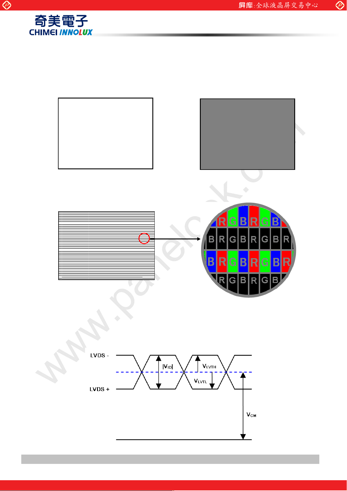
Pixel Arrangement RGB vertical stripe
Weight [g] TYP. 2155 g
Physical Size [mm] 955.04(W) × 545.66(H) × 2.00(D) Typ.
Display Mode Transmissive mode / Normallly black
Contrast Ratio 6000:1 Typ.
Glass thickness (Array / CF) [mm] 0.7 / 0.7
Viewing Angle (CR>20) +88/-88(H), +88/-88(V) Typ. (CR 20)Њ
Color Chromaticity
www.panelook.com
PRODUCT SPECIFICATION
(Typical value measure at CMO’s module)
(Typical value measure at CMO’s module)
R=(0.650, 0.327)
G=(0.297, 0.594)
B=(0.134,0.106)
W=(0.310, 0.357)
(Li
ht source is the standard light source “C” which is defined by
CIE and drivin
voltages.)
Cell Transparency [%] 4.8%
Polarizer Surface Treatment Anti-Glare coating (Haze 11%), Hard coating (3H)
voltages are based on suitable gamma
1.3 MECHANICAL SPECIFICATIONS
Item Min. Typ. Max. Unit Note
Weight 2105 2155 2205 g -
I/F connector mounting position
Note (1) Please refer to the attached drawings for more information of front and back outline dimensions.
Note (2) Connector mounting position
The mounting inclination of the connector makes the
screen center within ± 0.5mm as the horizontal.
(2)
Version 2.0 4 Date
The copyright belongs to CHIMEI InnoLux. Any unauthorized use is prohibited
One step solution for LCD / PDP / OLED panel application: Datasheet, inventory and accessory!
ΚΚΚΚ
08 Jul 2010
www.panelook.com
Page 5
Global LCD Panel Exchange Center
2. ABSOLUTE MAXIMUM RATINGS
2.1 ABSOLUTE RATINGS OF ENVIRONMENT
Item Symbol
Storage Temperature TST -20 +60 ºC (1)
Operating Ambient Temperature TOP 0 +50 ºC (1), (2)
Vibration (Non-Operating) V
Note (1) Temperature and relative humidity range is shown in the figure below.
www.panelook.com
PRODUCT SPECIFICATION
Value
Min. Max.
- 1.0 G (3), (4)
NOP
Unit Note
(a) 90 %RH Max. (Ta
(b) Wet-bulb temperature should be 39 ºC Max. (Ta > 40 ºC).
(c) No condensation.
Note (2) The maximum operating temperature is based on the test condition that the surface temperature of
display area is less than or equal to 65 ºC with LCD module alone in a temperature controlled chamber.
Thermal management should be considered in final product design to prevent the surface temperature of
display area from being over 65 ºC. The range of operating temperature may degrade in case of improper
thermal management in final product design.
Note (3) 10 ~ 200 Hz, 10 min, 1 time each X, Y, Z.
Note (4) At testing Vibration and Shock, the fixture in holding the module has to be hard and rigid enough so
that the module would not be twisted or bent by the fixture.
Љ
40 ºC).
Relative Humidity (%RH)
100
90
80
60
40
20
10
Operating Range
Storage Range
Temperature (ºC)
Version 2.0 5 Date
The copyright belongs to CHIMEI InnoLux. Any unauthorized use is prohibited
One step solution for LCD / PDP / OLED panel application: Datasheet, inventory and accessory!
80 60 -20 40 0 20 -40
ΚΚΚΚ
08 Jul 2010
www.panelook.com
Page 6
Global LCD Panel Exchange Center
www.panelook.com
PRODUCT SPECIFICATION
2.2 PACKAGE STORAGE
When storing modules as spares for a long time, the following precaution is necessary.
(a) Do not leave the module in high temperature, and high humidity for a long time. It is highly recommended to
store the module with temperature from 0 to 35 at normal humidity without condensation.
(b)The module shall be stored in dark place. Do not store the TFT-LCD module in direct sunlight or fluorescent
light.
к
2.3 ELECTRICAL ABSOLUTE RATINGS
2.3.1 TFT LCD MODULE
Item Symbol
Power Supply Voltage Vcc -0.3 13.5 V
Input Signal Voltage VIN -0.3 3.6 V
Min. Max.
Value
Unit Note
2.3.2 BACKLIGHT CONVERTER UNIT
Value
Item Symbol
Min. Max.
Unit Note
Ё
Lamp Voltage VW
Power Supply Voltage VBL 0 30 V (1)
Ё
Control Signal Level
Note (1) Permanent damage to the device may occur if maximum values are exceeded. Functional operation
should be restricted to the conditions described under normal operating conditions.
Note (2) No moisture condensation or freezing.
Note (3) The control signals include On/Off Control and Internal PWM Control.
-0.3 7 V (1), (3)
3000 VRMS
Version 2.0 6 Date
The copyright belongs to CHIMEI InnoLux. Any unauthorized use is prohibited
One step solution for LCD / PDP / OLED panel application: Datasheet, inventory and accessory!
ΚΚΚΚ
08 Jul 2010
www.panelook.com
Page 7
Global LCD Panel Exchange Center
www.panelook.com
PRODUCT SPECIFICATION
3. ELECTRICAL CHARACTERISTICS
3.1 TFT LCD MODULE
Ta = 25 ± 2 ºC
Value
Parameter Symbol
Unit Note
Min. Typ. Max.
Power Supply Voltage VCC 10.8 12 13.2 V (1)
Rush Current I
- - 4.17 A (2)
RUSH
White Pattern - - 1.27 1.65 A
Power
Horizontal
Supply
- - 1.32 1.72 A
(3)
Stripe
Current
Black Pattern - - 0.58 - A
Differential
Input High
Threshold
+100 - - mV
V
LVT H
Voltage
Differential
LVDS
interface
Input Low
Threshold
Voltage
Common Input
Voltage
Differential
input voltage
- - -100 mV
V
LVTL
V
1.0 1.2 1.4 V
CM
| 200 - 600 mV
|V
ID
(4)
Terminating
R
- 100 - ohm
Resistor
T
Input High
CMOS
interface
Threshold
Voltage
Input Low
Threshold
V
2.7 - 3.3 V
IH
0 - 0.7 V
V
IL
Voltage
Note (1) The module should be always operated within above ranges.
Note (2) Measurement Conditions:
Version 2.0 7 Date
The copyright belongs to CHIMEI InnoLux. Any unauthorized use is prohibited
ΚΚΚΚ
08 Jul 2010
One step solution for LCD / PDP / OLED panel application: Datasheet, inventory and accessory!
www.panelook.com
Page 8
Global LCD Panel Exchange Center
www.panelook.com
PRODUCT SPECIFICATION
GND
Vcc rising time is 470us
0.9Vcc
0.1Vcc
470us
Vcc
Version 2.0 8 Date
The copyright belongs to CHIMEI InnoLux. Any unauthorized use is prohibited
One step solution for LCD / PDP / OLED panel application: Datasheet, inventory and accessory!
ΚΚΚΚ
08 Jul 2010
www.panelook.com
Page 9
Global LCD Panel Exchange Center
Note (3) The specified power supply current is under the conditions at Vcc =12V, Ta = 25 ± 2 ºC, fv = 120 Hz,
whereas a power dissipation check pattern below is displayed.
www.panelook.com
PRODUCT SPECIFICATION
a. White Pattern
b. Black Pattern
Active Area
Active Area
c. Horizontal Pattern
Note (4) The LVDS input characteristics are as follows:
Version 2.0 9 Date
The copyright belongs to CHIMEI InnoLux. Any unauthorized use is prohibited
One step solution for LCD / PDP / OLED panel application: Datasheet, inventory and accessory!
ΚΚΚΚ
08 Jul 2010
www.panelook.com
Page 10

Global LCD Panel Exchange Center
_
)
_
)
_
)
_
)
4. BLOCK DIAGRAM OF INTERFACE
4.1 TFT LCD MODULE
www.panelook.com
PRODUCT SPECIFICATION
TFT LCD PANEL
(1920x3x1080)
X(R) Board X(L) Board
C Board
INPUT CONNECTOR
ڙࡶ
ڙࡶ
)) or equivalent
ڙࡶڙࡶ
CH4_0(+/-)
CH4_1(+/-)
CH4_2(+/-)
CH4_3(+/-)
CH4_4(+/-)
CH4
CLK(+/-
SELLVDS
VCC
GND
CH1_0(+/-)
CH1_1(+/-)
CH1_2(+/-)
CH1_3(+/-)
CH1_4(+/-)
CH1
CLK(+/-
(40550-8210,UJU(
CH2_0(+/-)
CH2_1(+/-)
CH2_2(+/-)
CH2_3(+/-)
CH2_4(+/-)
CH2
CLK(+/-
CH3_0(+/-)
CH3_1(+/-)
CH3_2(+/-)
CH3_3(+/-)
CH3_4(+/-)
CH3
CLK(+/-
Version 2.0 10 Date
The copyright belongs to CHIMEI InnoLux. Any unauthorized use is prohibited
ΚΚΚΚ
08 Jul 2010
One step solution for LCD / PDP / OLED panel application: Datasheet, inventory and accessory!
www.panelook.com
Page 11

Global LCD Panel Exchange Center
GNDGround
o connectio
6
at
data
STVScan d
start pulse
3
at
data
3
data latc
5
at
data
O3Data d
start pulse
5
at
data
5EIO
ata d
start pulse
6
data
6
L
Switc
data
GNDGround
8
GNDGround
8
GM18
Gamma power supply
9
ata d
9
G
Gamma power supply
0
ata d
50
GM16
Gamma power supply
GNDGround
51GM15
Gamma power supply
data
52G
Gamma power supply
3
data
53
GM13
Gamma power supply
data
54G
Gamma power supply
5
data
55
GM10
Gamma power supply
6
at
data
56
GM9
Gamma power supply
at
data
57GM7Gamma power supply
8
GNDGround
58
GM6
Gamma power supply
9
at
data
59
GM5
Gamma power supply
y
at
data
61GM3
Gamma power supply
at
data
62GM2Gamma power supp
y
3
data
63
GM1Gamma power supply
data
64GNDGround
5
GNDGround
65
ata d
supply
6
ata d
66
ata d
supply
ata d
ock
67GNDGround
8
GNDGround
68VC
com power supply
9
data
69VC
com power supply
30
data
0
GNDGround
3
data
ata d
supply
3
at
data
ata d
supply
33
at
data
3
GNDGround
3
0
at
data
supply
35
GNDGround
5
supply
36
GNDGround
6VGLScan d
supply
37OE1Scan d
output
Scan d
supply
38
OE2Scan d
output
Scan d
supply
39
CKVScan d
ock
9VGHScan d
supply
0PO
olarity
put
80
GNDGround
5. INTERFACE PIN CONNECTION
www.panelook.com
PRODUCT SPECIFICATION
5.1 TFT LCD MODULE
CN1(XL) Connector Pin Assignment
Pin Symbol Description Pin Symbol Description
1
2MLB
MLB6PB-P
4MLB
MLB5PB-P
MLB4N B-Path mini-LVDS
7 MLB4P B-Path mini-LVDS
MLBCKN D
1
11
12 MLB2N B-Path mini-LVDS
1
14 MLB1N B-Path mini-LVDS
1
1
17 MLB0PB-P
1
1
20 MLA6P A-Path mini-LVDS data 60 GM4 Gamma power suppl
21 MLA5NA-P
22 MLA5PA-P
2
24 MLA4P A-Path mini-LVDS
2
2
27 MLACKP D
2
2
1 MLA1N A-Path mini-LVDS
2MLA1P A-P
4MLA
4
MLBCKP D
MLB2P B-Path mini-LVDS
MLB1P B-Path mini-LVDS
MLB0NB-P
MLA6NA-P
MLA4N A-Path mini-LVDS
MLACKN D
MLA2N A-Path mini-LVDS
MLA2P A-Path mini-LVDS
MLA0NA-P
LP
NB-P
NB-P
PA-P
h mini-LVDS
h mini-LVDS
h mini-LVDS
h mini-LVDS
river clock4
river clock
h mini-LVDS
h mini-LVDS
h mini-LVDS
h mini-LVDS
h mini-LVDS
river clock
river cl
h mini-LVDS
h mini-LVDS
h mini-LVDS
river
river
river cl
inverting in
41 N.C.N
42
4
44 EI
4
4
47
4
7
71 VDDA D
72 VDDA D
7
74 VDD Logic power
7
7
77 VGL
78VGH
7
TP1 Mini-LVDS
4D
VDASE
M17
M14
M12
VDDAH D
VDDAL D
MV
MV
VDD Logic power
h for half-VDDA
n
river
h
river
river
l
river power
river power
river power
river power
riverpower
river power
river power
river power
Version 2.0 11 Date
The copyright belongs to CHIMEI InnoLux. Any unauthorized use is prohibited
One step solution for LCD / PDP / OLED panel application: Datasheet, inventory and accessory!
ΚΚΚΚ
08 Jul 2010
www.panelook.com
Page 12

Global LCD Panel Exchange Center
GNDGround
data
GHScan d
supply
data
3VGHScan d
supply
3
data
GLScan d
supply
at
data
5VGLScan d
supply
5
at
data
6
supply
6
GNDGround
ogic power supply
C-Pat
data
8
GNDGround
8MLC6
C-Pat
data
9
ata d
supply
9MLC5
C-Pat
data
0
ata d
supply
50MLC5
C-Pat
data
GNDGround
5
C
C-Pat
data
com power supply
5
C
C-Pat
data
3VC
com power supply
53
GNDGround
GNDGround
5
CC
ata d
5
ata d
supply
55MLCC
ata d
6
ata d
supply
56
GNDGround
GNDGround
5
C
C-Pat
data
8VSC
SC
supply
58MLC
C-Pat
data
9
Switc
59MLC
C-Pat
data
O3Data d
start pulse
6
C0
C-Pat
data
data latc
6
C0
C-Pat
data
3
STVScan d
start pulse
63
GNDGround
o connectio
64GM18
Gamma power supply
5PO
olarity
put
65
G
Gamma power supply
6
CKVScan d
ock
66
GM16
Gamma power supply
OE2Scan d
output
67GM15
Gamma power supply
8
OE1Scan d
output
68
G
Gamma power supply
9
GNDGround
69
GM13
Gamma power supply
30
at
data
0
G
Gamma power supply
3
6
at
data
GM10
Gamma power supply
3
5
at
data
GM9
Gamma power supply
33
at
data
3
GM7Gamma power supply
3
data
GM6
Gamma power supply
35
data
5
GM5
Gamma power supply
36
GNDGround
6
GM4Gamma power supply
3
C
ata d
3
Gamma power supply
38
ata d
8
GM2Gamma power supply
39
GNDGround
9
GM1Gamma power supply
0
data
80
GNDGround
CN1(XR) Connector Pin Assignment
Pin Symbol Description Pin Symbol Description
1
2V
4V
VDD Logic power
7VDD L
VDDA D
1
11
12 VCMV
1
14
1
1
17
1
1
20 EIO4 Data driver start pulse 60 MLC1P C-Path mini-LVDS data
21 EI
22 TP1 Mini-LVDS
2
24 N.C.N
2
2
27
2
2
1MLD
2MLD
4 MLD4N D-Path mini-LVDS
7MLD
4
Note (1) CN1 Connector Part No.: B-F,196225-80041,P-TWO(
VDDA D
MV
VDDAL D
VDDAH D
MV
VDASEL
LP
MLD6ND-P
PD-P
ND-P
MLD5PD-P
MLD4P D-Path mini-LVDS
KN D
MLDCKP D
MLD2N D-Path mini-LVDS
M Power
h for half-VDDA
h mini-LVDS
h mini-LVDS
h mini-LVDS
h mini-LVDS
www.panelook.com
PRODUCT SPECIFICATION
41 MLD2P D-Path mini-LVDS
river power
river power
river power
river power
river power
river power
river power
river power
river
h
river
n
inverting in
river cl
river
river
river clock77GM
river clock7
7
71
72
7
74
7
42 MLD1N D-Path mini-LVDS
4
44 MLD0ND-P
4
4
47 MLC6N
4
4
1ML
2ML
4ML
7ML
1ML
2ML
7
7
MLD1P D-Path mini-LVDS
MLD0PD-P
M17
M14
M12
ك࣑
)
P
N
P
4N
4P
KN D
KP D
2N
2P
1N
N
P
h mini-LVDS
h mini-LVDS
h mini-LVDS
h mini-LVDS
h mini-LVDS
h mini-LVDS
h mini-LVDS
h mini-LVDS
river clock
river clock
h mini-LVDS
h mini-LVDS
h mini-LVDS
h mini-LVDS
h mini-LVDS
Version 2.0 12 Date
The copyright belongs to CHIMEI InnoLux. Any unauthorized use is prohibited
One step solution for LCD / PDP / OLED panel application: Datasheet, inventory and accessory!
ΚΚΚΚ
08 Jul 2010
www.panelook.com
Page 13

Global LCD Panel Exchange Center
www.panelook.com
PRODUCT SPECIFICATION
System Board
Interface Voltage Level
VH > 3.0V
VL < 0.7V
Note (2) LVDS 4-port Data Mapping
Panel
1K ohm
IC
>20K ohm
Port Channel of LVDS Data Stream
1st Port First Pixel 1, 5, 9, ……1913, 1917
2nd Port Second Pixel 2, 6, 10, ….1914, 1918
3rd Port Third Pixel 3, 7, 11, ….1915, 1919
4th Port Fourth Pixel 4, 8, 12, ….1916, 1920
Version 2.0 13 Date
The copyright belongs to CHIMEI InnoLux. Any unauthorized use is prohibited
One step solution for LCD / PDP / OLED panel application: Datasheet, inventory and accessory!
ΚΚΚΚ
08 Jul 2010
www.panelook.com
Page 14

Global LCD Panel Exchange Center
5.2 LVDS INTERFACE
VESA Format : SELLVDS = L or Open
JEIDA Format : SELLVDS = H
www.panelook.com
PRODUCT SPECIFICATION
AR0~AR9: First Pixel R Data (9; MSB, 0; LSB)
AG0~AG9: First Pixel G Data (9; MSB, 0; LSB)
AB0~AB9: First Pixel B Data (9; MSB, 0; LSB)
DE : Data enable signal
DCLK : Data clock signal
RSV : Reserved
Version 2.0 14 Date
The copyright belongs to CHIMEI InnoLux. Any unauthorized use is prohibited
One step solution for LCD / PDP / OLED panel application: Datasheet, inventory and accessory!
ΚΚΚΚ
08 Jul 2010
www.panelook.com
Page 15

Global LCD Panel Exchange Center
5.3 COLOR DATA INPUT ASSIGNMENT
The brightness of each primary color (red, green and blue) is based on the 10-bit gray scale data input for the
color. The higher the binary input, the brighter the color. The table below provides the assignment of the color
versus data input.
www.panelook.com
PRODUCT SPECIFICATION
Data Signal
Basic
Colors
Gray
Scale
Of
Red
Color
Black
Red
Green
Blue
Cyan
Magenta
Yellow
White
Red (0) / Dark
Red (1)
Red (2)
:
:
Red (1021)
Red (1022)
Red Green Blue
R9R8R7R6R5R4R3R2R1R0G9G8G7G6G5G4G3G2G1G0B9B8B7B6B5B4B3B2B1B
0
0
0
0
0
0
0
0
0
0
0
0
0
0
0
0
0
0
0
0
0
0
0
0
0
0
0
0
0
0
0
0
0
0
0
0
0
0
0
0
0
0
0
0
0
0
0
0
1
1
1
1
1
1
1
1
1
1
0
0
0
0
0
0
0
0
0
1
1
1
1
1
1
1
1
1
1
0
0
0
0
0
0
0
0
0
0
1
1
1
1
1
1
1
1
1
0
0
0
0
0
0
0
0
0
0
0
0
0
0
0
0
0
0
0
0
1
1
1
1
1
1
1
1
1
1
1
1
1
1
1
1
1
1
1
0
0
0
0
0
0
0
0
0
0
1
1
1
1
1
1
1
1
1
0
0
0
0
0
0
0
0
0
0
1
1
1
1
1
1
1
1
1
1
0
0
0
0
0
0
0
0
0
1
1
1
1
1
1
1
1
1
1
1
1
1
1
1
1
1
1
1
1
1
1
1
1
1
1
1
1
1
1
1
1
1
1
1
1
1
1
1
1
1
1
1
1
1
1
1
1
1
0
0
0
0
0
0
0
0
0
0
0
0
0
0
0
0
0
0
0
0
0
0
0
0
0
0
0
0
0
0
0
0
0
0
0
1
0
0
0
0
0
0
0
0
0
0
0
0
0
0
0
0
0
0
0
0
0
0
0
1
0
0
0
0
0
0
0
0
:
:
:
:
:
:
:
:
:
:
:
:
:
:
:
:
:
:
:
:
:
:
:
;
:
:
:
:
:
:
:
:
:
:
:
:
:
:
:
:
:
:
0
0
0
0
0
0
0
0
0
0
0
0
0
1
0
1
1
1
1
1
1
1
1
0
0
0
0
0
0
0
0
0
0
0
0
0
0
1
1
1
1
1
1
1
1
1
0
0
0
0
0
0
0
:
:
:
:
:
:
0
0
0
0
0
0
0
0
0
0
0
0
0
0
0
0
0
0
:
:
:
:
:
:
0
0
0
0
0
0
0
0
0
0
1
1
1
0
1
0
0
0
:
:
0
0
Red (1023)
Green(0) / Dark
Green (1)
1
1
1
0
0
0
0
0
0
1
1
1
0
0
0
0
0
0
1
1
1
0
0
0
0
0
0
0
0
1
0
0
0
0
0
0
0
0
0
0
0
0
0
0
0
0
0
0
0
0
0
0
0
0
0
0
0
0
0
0
0
1
0
0
0
0
0
0
0
0
0
0
0
0
0
Green (2)
0
0
0
1
0
0
0
0
0
0
0
0
0
0
0
0
0
0
0
0
0
0
0
0
0
Gray
:
:
:
:
:
:
:
:
:
:
:
:
:
:
:
:
:
:
:
:
:
:
:
:
:
:
Scale
:
:
:
:
:
:
:
:
:
:
:
:
:
:
:
:
:
:
:
:
:
:
:
:
:
:
Of
Green (1021)
0
0
1
0
1
1
1
1
1
1
1
1
0
0
0
0
0
0
0
0
0
0
0
0
0
Green
Gray
Scale
Of
Blue
Green (1022)
Green (1023
Blue (0) / Dark
Blue (1)
Blue (2)
:
:
0
0
1
1
1
1
1
1
1
1
1
0
0
0
0
0
0
0
0
0
0
)
0
0
0
0
0
0
0
0
0
0
0
0
:
:
:
:
:
:
0
0
0
0
0
0
0
0
0
0
0
0
:
:
:
:
:
:
0
0
0
0
0
0
0
0
0
0
0
0
:
:
:
:
:
:
1
1
0
0
0
0
0
0
0
0
0
0
:
:
:
:
:
:
1
1
1
0
0
0
0
0
0
0
0
0
:
:
:
:
:
:
1
1
1
0
0
0
0
0
0
0
0
0
:
:
:
:
:
:
0
1
1
0
0
0
0
0
0
0
0
0
:
:
:
:
:
:
0
0
0
0
0
0
0
:
:
0
0
0
0
0
0
0
0
0
0
0
0
0
:
:
:
:
:
:
Version 2.0 15 Date
The copyright belongs to CHIMEI InnoLux. Any unauthorized use is prohibited
0
0
0
0
0
0
0
0
0
0
0
0
0
0
0
0
0
0
0
0
:
:
:
:
:
:
:
:
:
:
0
0
0
0
0
0
0
0
0
0
0
0
0
0
0
0
0
0
0
0
1
0
0
0
0
0
1
0
0
0
:
:
:
:
:
:
:
:
:
:
ΚΚΚΚ
08 Jul 2010
One step solution for LCD / PDP / OLED panel application: Datasheet, inventory and accessory!
www.panelook.com
Page 16

Global LCD Panel Exchange Center
www.panelook.com
PRODUCT SPECIFICATION
Blue (1021)
Blue (1022)
Blue (1023)
Note (1) 0: Low Level Voltage, 1: High Level Voltage
0
0
0
0
0
0
0
0
0
0
0
0
0
0
0
0
0
0
0
0
0
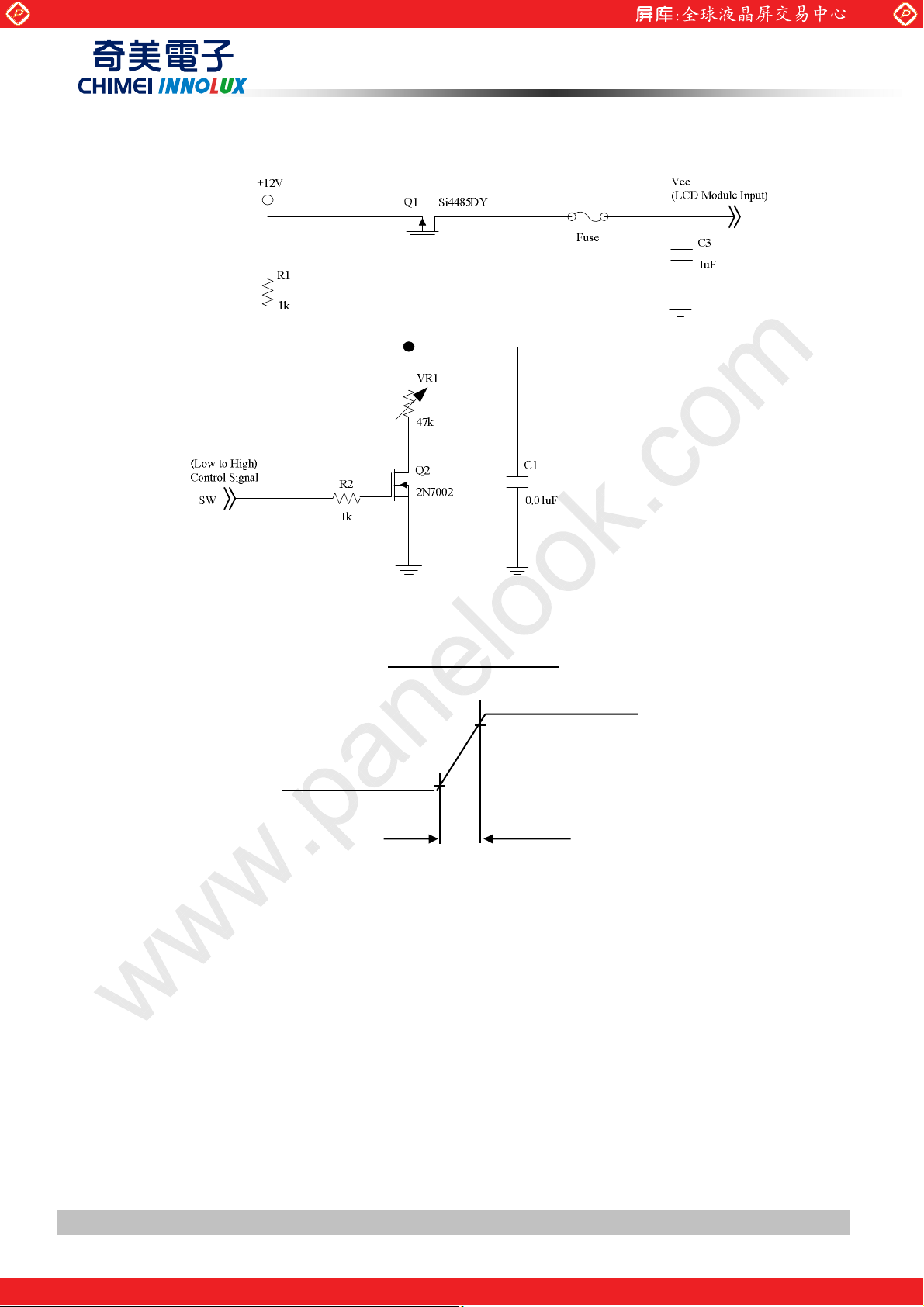
5.4 FLICKER (Vcom) ADJUSTMENT
(1) Adjustment Pattern:
2n line-inversion pattern was shown as below. If customer need below pattern, please directly contact with
Account FAE.
ʳ
˙˴˸ʳˡʳʳʳʳʳʳʳʳʳʳʳʳʳʳʳʳʳʳʳʳʳʳʳʳʳʳʳ˙˴˸ʳˡʾ˄ʳ
0
0
0
0
0
0
0
0
0
0
0
0
0
1
1
1
1
1
1
1
1
0
1
0
0
0
0
0
0
0
0
0
0
0
0
0
1
1
1
1
1
1
1
1
1
0
0
0
0
0
0
0
0
0
0
0
0
0
0
1
1
1
1
1
1
1
1
1
1
ʳʳʳʳʳʳʳʳʳʳʳʳʳʳ ʳ
!
(2) Adjustment method: (Digital V-com)
Programmable memory IC is used for Digital V-com adjustment in this model. CMI provide Auto Vcom tools to
adjust Digital V-com.The detail connection and setting instruction, please directly contact with Account FAE or
refer CMI Auto V-com adjustment OI. Below items is suggested to be ready before Digital V-com adjustment
in customer LCM line.
a. USB Sensor Board. (CMI Part number: 35-D044998)
b. Programmable software. (Multi Auto Vcom 1.0.6)
c. Document: Auto V-com adjustment suggestion OI. (CMI DCC number: 300019662)
Version 2.0 16 Date
The copyright belongs to CHIMEI InnoLux. Any unauthorized use is prohibited
One step solution for LCD / PDP / OLED panel application: Datasheet, inventory and accessory!
ΚΚΚΚ
08 Jul 2010
www.panelook.com
Page 17

Global LCD Panel Exchange Center
6. INTERFACE TIMING
6.1 INPUT SIGNAL TIMING SPECIFICATIONS
(Ta = 25 ± 2 ºC)
The input signal timing specifications are shown as the following table and timing diagram.
Signal Item Symbol Min. Typ. Max. Unit Note
Frequency
(=1/TC)
www.panelook.com
PRODUCT SPECIFICATION
F
clkin
60 74.25 80 MHz
LVDS
Receiver
Clock
LVDS
Receiver
Data
Vertical
Active
Display
Term
Horizontal
Active
Display
Input cycle to
T
- - 200 ps (3)
clkin_mo
F
rcl
-2% - F
F
d
clkin
+2% MHz
clkin
cycle jitter
Spread spectrum
modulation range
(4)
Spread spectrum
modulation frequency
SSM
- - 200 KHz
F
Setup Time Tlvsu 600 - - ps
(5)
Hold Time Tlvhd 600 - - ps
Fr5 TBD 100 TBD Hz
Frame Rate
TBD 120 TBD Hz
F
r6
(6)
Tv=Tvd+Tv
Total Tv 1115 1125 1135 Th
b
Ё
Ё
Display Tvd 1080 1080 1080 Th
Blank Tvb 35 45 55 Th
Th=Thd+T
Total Th 540 550 575 Tc
hb
Ё
Display Thd 480 480 480 Tc
Term
Blank Thb 60 70 95 Tc
Note (1) Since the module is operated in DE only mode, Hsync and Vsync input signals should be set to low
logic level. Otherwise, this module would operate abnormally.
Note (2) Please make sure the range of pixel clock has follow the below equation:
F
clkin(max)
F
r
5
Њ F
r
6
Ѽ Tv Ѽ Th
Ѽ Tv Ѽ Th Њ F
clkin(min)
Version 2.0 17 Date
The copyright belongs to CHIMEI InnoLux. Any unauthorized use is prohibited
One step solution for LCD / PDP / OLED panel application: Datasheet, inventory and accessory!
Ё
ΚΚΚΚ
08 Jul 2010
www.panelook.com
Page 18

Global LCD Panel Exchange Center
www.panelook.com
PRODUCT SPECIFICATION
INPUT SIGNAL TIMING DIAGRAM
Tvd
Tv
Tvb
DE
Th
DCLK
DE
Thd
DAT
Valid display data ( 480 clocks)
Note (3) The input clock cycle-to-cycle jitter is defined as below figures. Trcl = I T1 – TI
ʳ
Version 2.0 18 Date
The copyright belongs to CHIMEI InnoLux. Any unauthorized use is prohibited
One step solution for LCD / PDP / OLED panel application: Datasheet, inventory and accessory!
ΚΚΚΚ
08 Jul 2010
www.panelook.com
Page 19

Global LCD Panel Exchange Center
www.panelook.com
PRODUCT SPECIFICATION
Note (4) The SSCG (Spread spectrum clock generator) is defined as below figures.
Note (5) The LVDS timing diagram and setup/hold time is defined and showing as the following figures.
LVDS RECEIVER INTERFACE TIMING DIAGRAM
Tc
RXCLK+/-
RXn+/-
Tlvsu
Tlvhd
1T
3T
5T
7T
9T
11T
13T
14
Note (6) : (ODSEL) = H/L or open for 100/120 Hz frame rate. Please refer to 5.1 for detail information
14
14
14
14
14
14
Version 2.0 19 Date
The copyright belongs to CHIMEI InnoLux. Any unauthorized use is prohibited
One step solution for LCD / PDP / OLED panel application: Datasheet, inventory and accessory!
ΚΚΚΚ
08 Jul 2010
www.panelook.com
Page 20

Global LCD Panel Exchange Center
P
www.panelook.com
PRODUCT SPECIFICATION
6.2 POWER ON/OFF SEQUENCE
(Ta = 25 ± 2 ºC)
To prevent a latch-up or DC operation of LCD module, the power on/off sequence should be as the diagram
below.
10ms
50ms
50ms
ЉЉЉЉ
T4
0V
0V
T2
T3
0.5
ЉЉЉЉT1ЉЉЉЉ
ЉЉЉЉT2ЉЉЉЉ
0
ЉЉЉЉT3ЉЉЉЉ
0
500ms
LVDS Signals
0
0
ЉЉЉЉT7ЉЉЉЉ
ЉЉЉЉT8ЉЉЉЉ
Optio Signals
(SELLVDS,…)
0.1V
CC
Power On
T7
cc
0.1V
T
3
T1
T
2
T4
VA L I D
8
T
Backlight(Recommended)
500ms
100ms
ЉЉЉЉ
ЉЉЉЉ
T5
T6
50%
5
T
50%
6
T
Power ON/OFF Sequence
Note (1) The supply voltage of the external system for the module input should follow the definition of Vcc.
Note (2) Apply the lamp voltage within the LCD operation range. When the backlight turns on before the LCD
operation or the LCD turns off before the backlight turns off, the display may momentarily become
abnormal screen.
Note (3) In case of Vcc is in off level, please keep the level of input signals on the low or high impedance. If
T2<0,that maybe cause electrical overstress failure.
Note (4) T4 should be measured after the module has been fully discharged between power off and on period.
Note (5) Interface signal shall not be kept at high impedance when the power is on.
Version 2.0 20 Date
The copyright belongs to CHIMEI InnoLux. Any unauthorized use is prohibited
One step solution for LCD / PDP / OLED panel application: Datasheet, inventory and accessory!
ΚΚΚΚ
08 Jul 2010
www.panelook.com
Page 21

Global LCD Panel Exchange Center
www.panelook.com
PRODUCT SPECIFICATION
7. OPTICAL CHARACTERISTICS
7.1 TEST CONDITIONS
The LCD module should be stabilized at given temperature for 1 hour to avoid abrupt temperature change during
measuring. In order to stabilize the luminance, the measurement should be executed after lighting backlight for 1
hour in a windless room.
Item Symbol Value Unit
Ambient Temperature Ta
Ambient Humidity Ha
Supply Voltage VCC 12 V
Input Signal According to typical value in "3. ELECTRICAL CHARACTERISTICS"
Vertical Frame Rate Fr 120 Hz
25±2
50±10
7.2 OPTICAL SPECIFICATIONS
o
C
%RH
The relative measurement methods of optical characteristics are shown in 7.2. The following items should be
measured under the test conditions described in 7.1 and stable environment shown in 7.1.
Item Symbol Condition Min. Typ. Max. Unit Note
Contrast Ratio CR
Response Time
Center Transmittance T%
White Variation
Red
Color
Chromaticity
Viewing Angle
Note (1) Light source is the standard light source “C” which is defined by CIE and driving voltages are based on
Green
Blue
White
Horizontal
Vertical
Gray to
gray
δW
Rcx
Rcy 0.327
Gcx
Gcy 0.594
Bcx
Bcy 0.106
Wcx
Wcy
θx+
θ
-
x
θY+
-
θ
Y
θ
=0°, θY =0°
x
With CMO Module
=0°, θY =0°
θ
x
CS-2000
Standard light source “C
CR≥20
With CMO Module
4000 6000
-
- 4.8 - %
- - 1.3 -
Typ -
0.03
80 88
80
80
80
5.5 10
0.650
0.297
0.134
0.310
0.357
88 88 88 -
-
Typ +
0.03
-
- (2), (4)
ms (5)
(2), (8)
(2), (7)
-
-
-
(1),(6)
-
-
-
-
Deg. (2), (3)
suitable gamma voltages. The calculating method is as following
1. Measure Module’s and BLU’s spectrums. W, R, G, B are with signal input. BLU(for V420H2_LE3) is
supplied by CMO.
2. Calculate cell’s spectrum.
3. Calculate cell’s chromaticity by using the spectrum of standard light source “C”
Note (2) Light source is the BLU which is supplied by CMO and driving voltages are based on suitable gamma
voltages.
Note (3) Definition of Viewing Angle (θx, θy):
Viewing angles are measured by Conoscope Cono-80
Ǻ
Version 2.0 21 Date
The copyright belongs to CHIMEI InnoLux. Any unauthorized use is prohibited
One step solution for LCD / PDP / OLED panel application: Datasheet, inventory and accessory!
ΚΚΚΚ
08 Jul 2010
www.panelook.com
Page 22

Global LCD Panel Exchange Center
T
g
g
www.panelook.com
PRODUCT SPECIFICATION
Note (4) Definition of Contrast Ratio (CR):
θX- = 90º
6 o’clock
θ
y-
= 90º
The contrast ratio can be calculated by the following expression.
x-
y-
Normal
θx = θy = 0º
θy- θy+
θx−
θx+
y+
12 o’clock
direction
x+
θX+ = 90º
Contrast Ratio (CR) = L255 / L0
L 255: Luminance of gray level 255
L 0: Luminance of gray level 0
CR = CR (1), where CR (X) is corresponding to the Contrast Ratio of the point X at Figure in Note (7).
Note (5) Definition of Gray to Gray Switching Time:
100%
90%
Optical
Response
10%
0%
Gray to Gray
Switchin
ime
Gray to Gray
Switchin
The driving signal means the signal of gray level 0, 31, 63, 95, 127, 159, 191, 223 and 255.
Gray to gray average time means the average switching time of gray level 0, 31, 63, 95, 127, 159, 191, 223
and 255 to each other.
Version 2.0 22 Date
The copyright belongs to CHIMEI InnoLux. Any unauthorized use is prohibited
One step solution for LCD / PDP / OLED panel application: Datasheet, inventory and accessory!
ΚΚΚΚ
08 Jul 2010
www.panelook.com
Page 23

Global LCD Panel Exchange Center
W
L
Note (6) Measurement Setup:
The LCD module should be stabilized at given temperature for 1 hour to avoid abrupt temperature
change during measuring. In order to stabilize the luminance, the measurement should be
executed after lighting backlight for 1 hour in a windless room.
LCD M
odule
www.panelook.com
PRODUCT SPECIFICATION
LCD
P
anel
Field of View = 1º
500 mm
Note (7) Definition of White Variation (δW):
Measure the luminance of gray level 255 at 5 points
δW = Maximum [L (1), L (2), L (3), L (4), L (5)] / Minimum [L (1), L (2), L (3), L (4), L (5)]
D/4 D/2 3D/4
CS 2000 -
Horizontal Line
D
Light Shield Room
Ambient
(
uminance < 2
x)
lu
W/4
1 2
: Test Point
W/2
5
X
X=1 to 5
Vertical Line
3W/4
3 4
Note (8) Definition of Transmittance (T%):
The measurement based on BLU (for V420H2_LE3) with Three diffuser film.
Transmittance
=
Luminance of LCD module
Luminance of backlight
Active Area
Ϡ
100%
Version 2.0 23 Date
The copyright belongs to CHIMEI InnoLux. Any unauthorized use is prohibited
ΚΚΚΚ
08 Jul 2010
One step solution for LCD / PDP / OLED panel application: Datasheet, inventory and accessory!
www.panelook.com
Page 24

Global LCD Panel Exchange Center
8. DEFINITION OF LABELS
8.1 CMO MODULE LABEL
The barcode nameplate is pasted on each module as illustration, and its definitions are as following explanation.
www.panelook.com
PRODUCT SPECIFICATION
CHI MEI
OPTOELECTRONICS
V420H2 –PE1 Rev. XX
X X X X X X X Y M D L N N N N
(a) Model Name: V420H2-PE1
(b) Revision: Rev. XX, for example: A0, A1… B1, B2… or C1, C2…etc.
(c) Serial ID: X X
X X X X X Y M D L N N N N
Serial No.
Product Line
Year, Month, Date
CMO Internal Use
CMO Internal Use
Revision
E207943
MADE IN TAIWAN
GEMN
Serial ID includes the information as below:
(a) Manufactured Date: Year: 2001=1, 2002=2, 2003=3, 2004=4….2010=0, 2011=1, 2012=2....
Month: 1~9, A~C, for Jan. ~ Dec.
Day: 1~9, A~Y, for 1
(b) Revision Code: Cover all the change
(c) Serial No.: Manufacturing sequence of product
(d) Product Line: 1 -> Line1, 2 -> Line 2, …etc.
st
CMO Internal Use
to 31st, exclude I ,O, and U.
Version 2.0 24 Date
The copyright belongs to CHIMEI InnoLux. Any unauthorized use is prohibited
ΚΚΚΚ
08 Jul 2010
One step solution for LCD / PDP / OLED panel application: Datasheet, inventory and accessory!
www.panelook.com
Page 25

Global LCD Panel Exchange Center
9. PACKAGING
9.1 PACKING SPECIFICATIONS
(1) 9 LCD TV modules / 1 Box
(2) Box dimensions : 1225 (L) X 801 (W) X 234 (H)mm
(3) Weight : Approx. 34 Kg
www.panelook.com
PRODUCT SPECIFICATION
Version 2.0 25 Date
The copyright belongs to CHIMEI InnoLux. Any unauthorized use is prohibited
ΚΚΚΚ
08 Jul 2010
One step solution for LCD / PDP / OLED panel application: Datasheet, inventory and accessory!
www.panelook.com
Page 26

Global LCD Panel Exchange Center
9.2 PACKING METHOD
Figures 9-1 and 9-2 are the packing method
www.panelook.com
PRODUCT SPECIFICATION
Figure.10-2 packing method
Version 2.0 26 Date
The copyright belongs to CHIMEI InnoLux. Any unauthorized use is prohibited
One step solution for LCD / PDP / OLED panel application: Datasheet, inventory and accessory!
ΚΚΚΚ
08 Jul 2010
www.panelook.com
Page 27

Global LCD Panel Exchange Center
www.panelook.com
PRODUCT SPECIFICATION
10. PRECAUTIONS
10.1 ASSEMBLY AND HANDLING PRECAUTIONS
(1) Do not apply rough force such as bending or twisting to the module during assembly.
(2) It is recommended to assemble or to install a module into the user’s system in clean working areas. The
dust and oil may cause electrical short or worsen the polarizer.
(3) Do not apply pressure or impulse to the module to prevent the damage of LCD panel and backlight.
(4) Always follow the correct power-on sequence when the LCD module is turned on. This can prevent the
damage and latch-up of the CMOS LSI chips.
(5) Do not plug in or pull out the I/F connector while the module is in operation.
(6) Do not disassemble the module.
(7) Use a soft dry cloth without chemicals for cleaning, because the surface of polarizer is very soft and
easily scratched.
(8) Moisture can easily penetrate into LCD module and may cause the damage during operation.
(9) High temperature or humidity may deteriorate the performance of LCD module. Please store LCD
modules in the specified storage conditions.
(10) When ambient temperature is lower than 10ºC, the display quality might be reduced. For example, the
response time will become slow, and the starting voltage of LED light bar will be higher than that of room
temperature.
10.2 SAFETY PRECAUTIONS
(1) The startup voltage of a backlight is over 1000 Volts. It may cause an electrical shock while assembling
with the converter. Do not disassemble the module or insert anything into the backlight unit.
(2) If the liquid crystal material leaks from the panel, it should be kept away from the eyes or mouth. In case
of contact with hands, skin or clothes, it has to be washed away thoroughly with soap.
(3) After the module’s end of life, it is not harmful in case of normal operation and storage.
Version 2.0 27 Date
The copyright belongs to CHIMEI InnoLux. Any unauthorized use is prohibited
One step solution for LCD / PDP / OLED panel application: Datasheet, inventory and accessory!
ΚΚΚΚ
08 Jul 2010
www.panelook.com
Page 28

Global LCD Panel Exchange Center
11. MECHANICAL CHARACTERISTICS
www.panelook.com
PRODUCT SPECIFICATION
ڻႝηިҽԖϦљ
CHI MEI
Version 2.0 28 Date
The copyright belongs to CHIMEI InnoLux. Any unauthorized use is prohibited
One step solution for LCD / PDP / OLED panel application: Datasheet, inventory and accessory!
ΚΚΚΚ
08 Jul 2010
www.panelook.com
 Loading...