

Page 1
Global LCD Panel Exchange Center
MODEL NO.: V420H2
www.panelook.com
PRODUCT SPECIFICATION
ϭʳ Tentative Specification
ϭʳ Preliminary Specification
Ϯʳ Approval Specification
SUFFIX: LE4
Customer:
APPROVED BY SIGNATURE
Name / Title
Note
Please return 1 copy for your confirmation with your signature
and comments.
Approved By Checked By Prepared By
Chao-Chun Chung Ken Wu Peggi Chiu
Version 2.0 1 DateΚΚΚΚ27 May 2010
The copyright belongs to CHIMEI InnoLux. Any unauthorized use is prohibited
One step solution for LCD / PDP / OLED panel application: Datasheet, inventory and accessory!
www.panelook.com
Page 2
Global LCD Panel Exchange Center
www.panelook.com
PRODUCT SPECIFICATION
CONTENTS
1. GENERAL DESCRIPTION .....................................................................................................................................5
1.1 OVERVIEW.................................................................................................................................................. 5
1.2 FEATURES ..................................................................................................................................................5
1.3 APPLICATION.............................................................................................................................................. 5
1.4 GENERAL SPECIFICATI0NS....................................................................................................................... 5
1.5 MECHANICAL SPECIFICATIONS................................................................................................................ 5
2.1 ABSOLUTE RATINGS OF ENVIRONMENT .........................................................................................................6
2.2 PACKAGE STORAGE ..........................................................................................................................................6
2.3 ELECTRICAL ABSOLUTE RATINGS ...................................................................................................................7
2.3.1 TFT LCD MODULE............................................................................................................................................7
2.3.2 BACKLIGHT UNIT.............................................................................................................................................7
3. ELECTRICAL CHARACTERISTICS .......................................................................................................................8
3.1 TFT LCD MODULE ...................................................................................................................................... 8
3.2 BACKLIGHT CONVERTER UNIT............................................................................................................... 11
3.2.1 LED LIGHT BARCHARACTERISTICS (Ta = 25 ± 2 ºC) ..................................................................11
3.2.2 CONVERTER CHARACTERISTICS (Ta = 25 ± 2 ºC) ...................................................................... 11
3.2.3 CONVERTER INTERFACE CHARACTERISTICS ...........................................................................12
4. BLOCK DIAGRAM OF INTERFACE.....................................................................................................................14
4.1 TFT LCD MODULE .................................................................................................................................... 14
5. INTERFACE PIN CONNECT ION ..........................................................................................................................15
5.1 TFT LCD MODULE .................................................................................................................................... 15
5.2 BACKLIGHT UNIT ..................................................................................................................................... 19
5.3 CONVERTER UNIT .................................................................................................................................... 20
5.4 BLOCK DIAGRAM OF INTERFACE...........................................................................................................21
5.5 LVDS INTERFACE ..................................................................................................................................... 23
6. INTERFACE TIMING ............................................................................................................................................26
6.1 INPUT SIGNAL TIMING SPECIFICATIONS ...............................................................................................26
6.2 POWER ON/OFF SEQUENCE ................................................................................................................... 27
6.2 POWER ON/OFF SEQUENCE ................................................................................................................... 28
7. OPTICAL CHARACTERISTICS............................................................................................................................29
7.1 TEST CONDITIONS ................................................................................................................................... 29
7.2 OPTICAL SPECIFICATIONS...................................................................................................................... 30
8. DEFINITION OF LABELS.....................................................................................................................................33
8.1 CMO MODULE LABEL .............................................................................................................................. 33
9. PACKAGING ........................................................................................................................................................35
9.1 PACKING SPECIFICATIONS ..................................................................................................................... 35
9.2 PACKING METHOD................................................................................................................................... 35
One step solution for LCD / PDP / OLED panel application: Datasheet, inventory and accessory!
www.panelook.com
Page 3
Global LCD Panel Exchange Center
www.panelook.com
PRODUCT SPECIFICATION
10. PRECAUTIONS..................................................................................................................................................37
10.1 ASSEMBLY AND HANDLING PRECAUTIONS ........................................................................................ 37
10.2 SAFETY PRECAUTIONS......................................................................................................................... 37
11. MECHANICAL CHARACTERISTICS..................................................................................................................38
Appendix – TWO Wire BUS INTRODUCTION...........................................................................................................40
A.1 PIN ASSIGNMENT..................................................................................................................................... 40
A.2 I2C BUS APPLICATION NOTE................................................................................................................... 40
A.3 TWO WIRE BUS DEVICE ADDRESS......................................................................................................... 41
A.4 TWO WAY TO CONTROL THE TWO WIRE BUS........................................................................................41
A.5 TWO WIRE BUS COMMAND TABLE ......................................................................................................... 43
Version 2.0 3 DateΚΚΚΚ27 May 2010
The copyright belongs to CHIMEI InnoLux. Any unauthorized use is prohibited
One step solution for LCD / PDP / OLED panel application: Datasheet, inventory and accessory!
www.panelook.com
Page 4
Global LCD Panel Exchange Center
Version Date Page(New) Section Description
www.panelook.com
PRODUCT SPECIFICATION
REVISION HISTORY
Ver. 2.0 May 27, 2010 All
All
The specification was first issued.
Version 2.0 4 DateΚΚΚΚ27 May 2010
The copyright belongs to CHIMEI InnoLux. Any unauthorized use is prohibited
One step solution for LCD / PDP / OLED panel application: Datasheet, inventory and accessory!
www.panelook.com
Page 5
Global LCD Panel Exchange Center
1. GENERAL DESCRIPTION
1.1 OVERVIEW
V420H2- LE4 is a 42” TFT Liquid Crystal Display module with LED Backlight and 2 ch-LVDS interface.
This module supports 1920 x 1080 Full HDTV format and can display 1.07G colors ( 8-bit+ FRC). The
converter module for backlight is built-in.
1.2 FEATURES
- High brightness (450 nits)
- Ultra-high contrast ratio (6000:1)
- Faster response time (gray to gray average 5.5 ms)
High color saturation NTSC 72% (72%)
-
- Ultra wide viewing angle : 176(H)/176(V) (CR≥20) with Super MVA technology
www.panelook.com
PRODUCT SPECIFICATION
- DE (Data Enable) only mode
- LVDS (Low Voltage Differential Signaling) interface
1.3 APPLICATION
- TFT LCD TVs
- Multi-Media Display
1.4 GENERAL SPECIFICATI0NS
Item Specification Unit Note
Active Area 930.24 (H) x 523.26 (V) (42" diagonal) mm
Bezel Opening Area 937.24 (H) x 530.26 (V) mm
Driver Element a-si TFT active matrix -
Pixel Number 1920 x R.G.B. x 1080 pixel
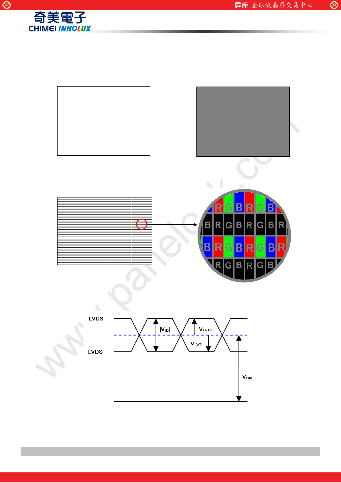
Pixel Pitch (Sub Pixel) 0.1615 (H) x 0.4845 (V) mm
Pixel Arrangement RGB vertical stripe -
Display Colors 1.07G color
Display Operation Mode Transmissive mode / Normally Black -
Surface Treatment
Anti-Glare Coating (Haze 11%)
Hard Coating (3H)
-
(1)
1.5 MECHANICAL SPECIFICATIONS
Item Min. Typ. Max. Unit Note
Horizontal(H) - 973.24 - mm (1)
Vertical(V) - 566.26 - mm (1)
Module Size
Note (1) Please refer to the attached drawings for more information of front and back outline dimensions.
Depth(D)
Depth(D)
Weight 7950
-
24.6 25.6 26.6
10.8
-
mm
mm To converter
cover
Version 2.0 5 DateΚΚΚΚ27 May 2010
The copyright belongs to CHIMEI InnoLux. Any unauthorized use is prohibited
One step solution for LCD / PDP / OLED panel application: Datasheet, inventory and accessory!
www.panelook.com
Page 6

Global LCD Panel Exchange Center
2. ABSOLUTE MAXIMUM RATINGS
2.1 ABSOLUTE RATINGS OF ENVIRONMENT
Item Symbol
Storage Temperature TST -20 +60 ºC (1)
Operating Ambient Temperature TOP 0 +50 ºC (1), (2)
Shock (Non-Operating) S
Vibration (Non-Operating) V
Note (1) Temperature and relative humidity range is shown in the figure below.
(a) 90 %RH Max. (Ta Љ 40 ºC).
(b) Wet-bulb temperature should be 39 ºC Max. (Ta > 40 ºC).
(c) No condensation.
Note (2) The maximum operating temperature is based on the test condition that the surface temperature of
display area is less than or equal to 65 ºC with LCD module alone in a temperature controlled chamber.
www.panelook.com
PRODUCT SPECIFICATION
Value
Min. Max.
- 35 G (3), (5)
NOP
- 1.0 G (4), (5)
NOP
Unit Note
Thermal management should be considered in final product design to prevent the surface temperature of
display area from being over 65 ºC. The range of operating temperature may degrade in case of improper
thermal management in final product design.
Note (3) 11 ms, half sine wave, 1 time for ± X, ± Y, ± Z.
Note (4) 10 ~ 200 Hz, 10 min, 1 time each X, Y, Z.
Note (5) At testing Vibration and Shock, the fixture in holding the module has to be hard and rigid enough so
that the module would not be twisted or bent by the fixture.
Relative Humidity (%RH)
100
90
80
60
Operating Range
40
20
10
Storage Range
80 60 -20 40 0 20 -40
Temperature (ºC)
2.2 PACKAGE STORAGE
Version 2.0 6 DateΚΚΚΚ27 May 2010
The copyright belongs to CHIMEI InnoLux. Any unauthorized use is prohibited
One step solution for LCD / PDP / OLED panel application: Datasheet, inventory and accessory!
www.panelook.com
Page 7
Global LCD Panel Exchange Center
When storing modules as spares for a long time, the following precaution is necessary.
(a) Do not leave the module in high temperature, and high humidity for a long time. It is highly recommended to
store the module with temperature from 0 to 35 at normal humidity without condensation.к
(b)The module shall be stored in dark place. Do not store the TFT-LCD module in direct sunlight or fluorescent
light.
2.3 ELECTRICAL ABSOLUTE RATINGS
2.3.1 TFT LCD MODULE
Item Symbol
Power Supply Voltage Vcc -0.3 13.5 V
Input Signal Voltage VIN -0.3 3.6 V
www.panelook.com
PRODUCT SPECIFICATION
Value
Min. Max.
Unit Note
2.3.2 BACKLIGHT UNIT
Item Symbol
Light Bar Voltage VW Ta = 25 к - - 60 V
Converter Input Voltage VBL - 0 - 30 V
Control Signal Level - - -0.3 - 7 V
Note (1) Permanent damage to the device may occur if maximum values are exceeded. Functional operation
should be restricted to the conditions described under normal operating conditions.
Note (2) No moisture condensation or freezing.
Note (3) The control signals include On/Off Control and Internal PWM Control.
Te st
Condition
Min. Type Max. Unit Note
RMS
Version 2.0 7 DateΚΚΚΚ27 May 2010
The copyright belongs to CHIMEI InnoLux. Any unauthorized use is prohibited
One step solution for LCD / PDP / OLED panel application: Datasheet, inventory and accessory!
www.panelook.com
Page 8
Global LCD Panel Exchange Center
3. ELECTRICAL CHARACTERISTICS
www.panelook.com
PRODUCT SPECIFICATION
3.1 TFT LCD MODULE
Ta = 25 ± 2 ºC
Parameter Symbol
Power Supply Voltage V
Rush Current I
White Pattern - - 1.81 A
Power
Horizontal
Supply
Stripe
Current
Black Pattern - - 0.58 - A
Differential
Input High
Threshold
V
Voltage
Differential
LVDS
interface
Input Low
Threshold
Voltage
Common Input
V
Voltage
Differential
input voltage
Terminating
Resistor
Value
Unit Note
Min. Typ. Max.
CC
RUSH
10.8 12 13.2 V (1)
- - 4.2 A (2)
- - 1.54 A
+100 - - mV
LVT H
LVTL
V
CM
| 200 - 600 mV
|V
ID
R
T
- - -100 mV
1.0 1.2 1.4 V
- 100 - ohm
(3)
(4)
Input High
CMOS
interface
Threshold
Voltage
Input Low
Threshold
V
IH
V
IL
2.7 - 3.3 V
0 - 0.7 V
Voltage
Note (1) The module should be always operated within above ranges.
Note (2) Measurement Conditions:
Version 2.0 8 DateΚΚΚΚ27 May 2010
The copyright belongs to CHIMEI InnoLux. Any unauthorized use is prohibited
One step solution for LCD / PDP / OLED panel application: Datasheet, inventory and accessory!
www.panelook.com
Page 9
Global LCD Panel Exchange Center
www.panelook.com
PRODUCT SPECIFICATION
Vcc rising time is 470us
Vcc
0.9Vcc
0.1Vcc
GND
470us
Note (3) The specified power supply current is under the conditions at Vcc =12V, Ta = 25 ± 2 ºC, fv = 120 Hz,
whereas a power dissipation check pattern below is displayed.
Version 2.0 9 DateΚΚΚΚ27 May 2010
The copyright belongs to CHIMEI InnoLux. Any unauthorized use is prohibited
One step solution for LCD / PDP / OLED panel application: Datasheet, inventory and accessory!
www.panelook.com
Page 10
Global LCD Panel Exchange Center
www.panelook.com
PRODUCT SPECIFICATION
a. White Pattern
Active Area
c. Horizontal Pattern
b. Black Pattern
Active Area
Note (4) The LVDS input characteristics are as follows:
Version 2.0 10 DateΚΚΚΚ27 May 2010
The copyright belongs to CHIMEI InnoLux. Any unauthorized use is prohibited
One step solution for LCD / PDP / OLED panel application: Datasheet, inventory and accessory!
www.panelook.com
Page 11
Global LCD Panel Exchange Center
3.2 BACKLIGHT CONVERTER UNIT
3.2.1 LED LIGHT BARCHARACTERISTICS(Ta = 25 ± 2 ºC)
Parameter Symbol
Forward Voltage V
LED Current I
Life time
Note (1) The lifetime is defined as the time which luminance of the LED decays to 50% compared to the
W
L
-
www.panelook.com
PRODUCT SPECIFICATION
Value
Min. Typ. Max.
3.0 3.5
- 120
30,000 - -
Unit Note
V
I
RMS
mA
RMS
Hrs (1)
=120.0mA
L
initial value, Operating condition: Continuous operating at Ta = 252к, I
(
3.2.2 CONVERTER CHARACTERISTICS
Parameter Symbol
Power Consumption PBL -
Power Supply Voltage VBL 22.8 24.0 25.2 VDC
Power Supply Current IBL - 3.96 4.17 A Non Dimming
Dimming Frequency FB 150 160 170 Hz
Minimum Duty Ratio DMIN 5 10 - % (1)
Note (1) 5% minimum duty ratio is only valid for electrical operation.
Ta = 25 ± 2 ºC)
Value
Min. Typ. Max.
95 100
=120mA
L
Unit Note
W IL =120mA
Version 2.0 11 DateΚΚΚΚ27 May 2010
The copyright belongs to CHIMEI InnoLux. Any unauthorized use is prohibited
One step solution for LCD / PDP / OLED panel application: Datasheet, inventory and accessory!
www.panelook.com
Page 12
Global LCD Panel Exchange Center
3.2.3 CONVERTER INTERFACE CHARACTERISTICS
External dimming: 150Hz~170Hz, duty ratio: 10%~100%
www.panelook.com
PRODUCT SPECIFICATION
Parameter Symbol
ON
On/Off Control Voltage
OFF
Internal PWM Control
Voltage
External PWM Control
Voltage
Status Signal
VBL Rising Time Tr1
VBL Falling Time Tf1
Control Signal Rising Time Tr
MAX
MIN
LO
LO
VBLON
VIPWM
HI
VEPWM
HI
Status
0
0
0
30
30
Value
Ё
Ё
Ё
0
Ё
Ё
Ё
ЁЁ
ЁЁ
Te st
Condition
Ё
Ё
Ё
ЁЁ
Ё
Ё
Ё
Ё
Ё
Ё
ЁЁЁ
Min. Typ. Max.
2.0
3.15
2.0
3.0 3.3 3.6 V Normal
Unit Note
5.0 V
0.8 V
3.45
Ё
5.0 V Duty on
0.8 V Duty off
0.8 V Abnormal
100 ms
maximum duty ratio
V
minimum duty ratio
V
ms
10%-90%V
ms
BL
Control Signal Falling Time Tf
PWM Signal Rising Time TPWMR
PWM Signal Falling Time TPWMF
Input Impedance Rin
PWM Delay Time TPWM
T
BLON Delay Time
BLON Off Time Toff
Note (1) The Dimming signal should be valid before backlight turns on by BLON signal. It is inhibited to
change the internal/external PWM signal during backlight turn on period.
Note (2) The power sequence and control signal timing are shown in the following figure. For a certain
reason, the converter has a possibility to be damaged with wrong power sequence and control
signal timing.
Note (3) While system is turned ON or OFF, the power sequences must follow as below descriptions:
Turn ON sequence: VBL Ш PWM signal Ш BLON
on
T
on1
ЁЁЁ
ЁЁЁ
ЁЁЁ
Ё
Ё
Ё
Ё
Ё
1
100
300
300
300
ЁЁ
ЁЁ
ЁЁ
ЁЁ
ЁЁ
100 ms
50 us
50 us
MΩ
ms
ms
ms
ms
Turn OFF sequence: BLOFF Ш PWM signal Ш VBL
Version 2.0 12 DateΚΚΚΚ27 May 2010
The copyright belongs to CHIMEI InnoLux. Any unauthorized use is prohibited
One step solution for LCD / PDP / OLED panel application: Datasheet, inventory and accessory!
www.panelook.com
Page 13
Global LCD Panel Exchange Center
www.panelook.com
PRODUCT SPECIFICATION
V
V
V
BL
V
BLON
EPWM
IPWM
9
Toff
%/
Tf1
9
%/
Tr1
9
%/
9
%/
2.0V
0.8V
Ton
Ton1
0
0
Backlight on duration
Tr
Tf
Ext. Dimming Function
T
PWMR
2.0V
0
0.8V
T
PWM
T
PWMF
Floating
3.3V
0
Floating
Int. Dimming Function
V
W
External
PWM
Period
External
PWM Duty
100%
Minimun
Duty
Version 2.0 13 DateΚΚΚΚ27 May 2010
The copyright belongs to CHIMEI InnoLux. Any unauthorized use is prohibited
One step solution for LCD / PDP / OLED panel application: Datasheet, inventory and accessory!
www.panelook.com
Page 14
Global LCD Panel Exchange Center
)
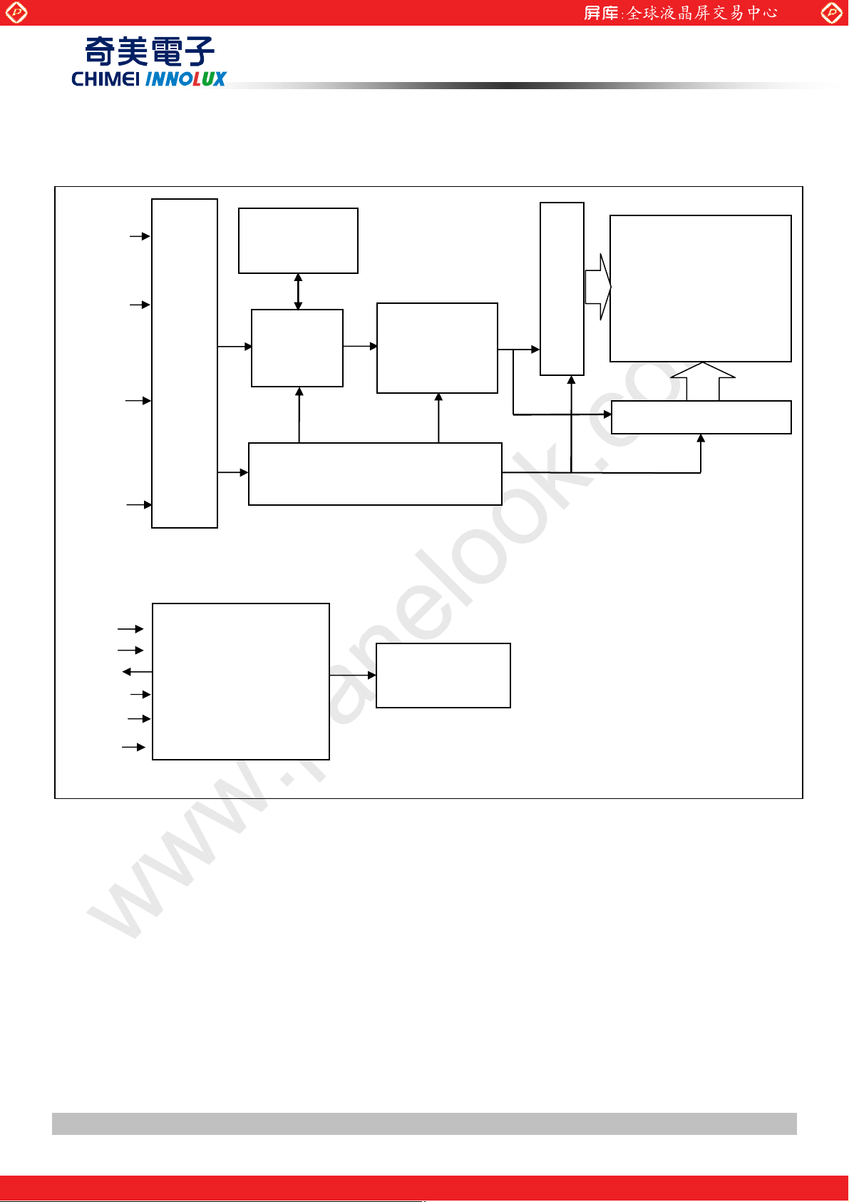
4. BLOCK DIAGRAM OF INTERFACE
4.1 TFT LCD MODULE
ODD_RIN0+/ODD_RIN1+/ODD_RIN2+/ODD_RIN3+/ODD_RIN4+/ODD_CLK+/-
EVEN_RIN0+/EVEN_RIN1+/EVEN_RIN2+/EVEN_RIN3+/EVEN_RIN4+/EVEN_CLK+/-
RPF
MEN
MCFG0
MCFG 1
LVDS8b
GV_mode
SELLVDS
ODSE
SCL
VCC
GND
(FI-RE51S-HF (JAE)) or equivalent
INPUT CONNECTOR
FRAME
BUFFE
MEM
DC/DC CONVERTER
& REFERENCE VOLTAGE
www.panelook.com
PRODUCT SPECIFICATION
SCAN DRIVER
TFT LCD PANEL
(1920x3x1080)
TIMING
CONTROLLER
Data Driver (mini-LVDS
GENERATOR
VB
GND
Statu s
A_DI M
I_PWM
BLON
CONVERTER
CONNECTOR
CN1:S14B-PH-SM4
-TB(D)(LF) or
equivalent
BACKLIGHT
UNIT
Version 2.0 14 DateΚΚΚΚ27 May 2010
The copyright belongs to CHIMEI InnoLux. Any unauthorized use is prohibited
One step solution for LCD / PDP / OLED panel application: Datasheet, inventory and accessory!
www.panelook.com
Page 15
Global LCD Panel Exchange Center
5. INTERFACE PIN CONNECTION
5.1 TFT LCD MODULE
CNF1 Connector Pin Assignment: (FI-RE51S-HF(JAE) or equivalent)
Pin Name Description Note
1 RPF Reverse picture function (default low) 8
2 MEN MEMC function selection 5
3 MCFG0 MEMC function selection 5
4 MCFG1 MEMC function selection 5
5 LVDS8b 8bit/10bit LVDS input selection 6
6 GV_mode Graphic / Video mode selection 7
7 SELLVDS LVDS data format Selection 3
8 SCL I2C CLK Signal ʳ
9 SDA. I2C Data Signal ʳ
10 ODSEL Overdrive Lookup Table Selection 4
11 GND Ground ʳ
12 ERX0- 2nd pixel Negative LVDS differential data input. Channel 0 ʳ
13 ERX0+ 2nd pixel Positive LVDS differential data input. Channel 0 ʳ
14 ERX1- 2nd pixel Negative LVDS differential data input. Channel 1 ʳ
15 ERX1+ 2nd pixel Positive LVDS differential data input. Channel 1 ʳ
16 ERX2- 2nd pixel Negative LVDS differential data input. Channel 2 ʳ
17 ERX2+ 2nd pixel Positive LVDS differential data input. Channel 2 ʳ
18 GND Ground ʳ
19 ECLK- 2nd pixel Negative LVDS differential clock input. ʳ
20 ECLK+ 2nd pixel Positive LVDS differential clock input. ʳ
21 GND Ground ʳ
22 ERX3- 2nd pixel Negative LVDS differential data input. Channel 3 ʳ
23 ERX3+ 2nd pixel Positive LVDS differential data input. Channel 3 ʳ
24 ERX4- 2nd pixel Negative LVDS differential data input. Channel 4 ʳ
25 ERX4+ 2nd pixel Positive LVDS differential data input. Channel 4 ʳ
26 N.C. No Connection 2
27 N.C. No Connection 2
28 ORX0- 1st pixel Negative LVDS differential data input. Channel 0 ʳ
29 ORX0+ 1st pixel Positive LVDS differential data input. Channel 0 ʳ
30 ORX1- 1st pixel Negative LVDS differential data input. Channel 1 ʳ
31 ORX1+ 1st pixel Positive LVDS differential data input. Channel 1 ʳ
32 ORX2- 1st pixel Negative LVDS differential data input. Channel 2 ʳ
33 ORX2+ 1st pixel Positive LVDS differential data input. Channel 2 ʳ
34 GND Ground ʳ
35 OCLK- 1st pixel Negative LVDS differential clock input. ʳ
36 OCLK+ 1st pixel Positive LVDS differential clock input. ʳ
37 GND Ground ʳ
38 ORX3- 1st pixel Negative LVDS differential data input. Channel 3 ʳ
39 ORX3+ 1st pixel Positive LVDS differential data input. Channel 3 ʳ
40 ORX4- 1st pixel Negative LVDS differential data input. Channel 4 ʳ
www.panelook.com
PRODUCT SPECIFICATION
Version 2.0 15 DateΚΚΚΚ27 May 2010
The copyright belongs to CHIMEI InnoLux. Any unauthorized use is prohibited
One step solution for LCD / PDP / OLED panel application: Datasheet, inventory and accessory!
www.panelook.com
Page 16

Global LCD Panel Exchange Center
41 ORX4+ 1st pixel Positive LVDS differential data input. Channel 4 ʳ
42 N.C. No Connection 2
43 N.C. No Connection 2
44 GND Ground ʳ
45 GND Ground ʳ
46 GND Ground ʳ
47 N.C. No Connection 2
48 VCC +12V power supply ʳ
49 VCC +12V power supply ʳ
50 VCC +12V power supply ʳ
51 VCC +12V power supply ʳ
Note (1) LVDS connector pin orderdefined as follows
www.panelook.com
PRODUCT SPECIFICATION
Note (2) Reserved for internal use. Please leave it open.
Note (3)
SELLVDS Mode
L(default)
H
L: Connect to GND, H: Connect to +3.3V
Note (4) Overdrive lookup table selection. The overdrive lookup table should be selected in accordance with the
frame rate to optimize image quality.
VESA
JEIDA
ODSEL Description
L(default)
H
Lookup table was optimized for 60 Hz frame rate input.
Lookup table was optimized for 50 Hz frame rate input.
L: Connect to GND, H: Connect to +3.3V
Version 2.0 16 DateΚΚΚΚ27 May 2010
The copyright belongs to CHIMEI InnoLux. Any unauthorized use is prohibited
One step solution for LCD / PDP / OLED panel application: Datasheet, inventory and accessory!
www.panelook.com
Page 17

Global LCD Panel Exchange Center
www.panelook.com
PRODUCT SPECIFICATION
Note (5) Motion Engine (ME) Level & Demo Function Table
Motion engine level must be adjusted after video mode is selected (or entered).
ʳʳAdjusting the motion engine level in graphic mode has no effect
MEN MCFG1 MCFG0 Notes
Blanking
0 0 0 (a)
disable
Blanking
Auto blanking 0 0 1 (b)
Blanking
0 1 0 (c)
enable
Effect of ME De blur De judder Halo
Demo mode (d) 0 1 1 Demo Window
Strong 1 0 0 Enable Strong Strong
Medium(Defaul
1 0 1 Enable Normal Normal
t)
ME Level
Weak 1 1 0 Enable Weak ×
OFF 1 1 1 × × ×
(e) (f) (g)
(a) Module re-starts processing video signals from Frontend scaler control board.
(b) During sync unstable period such as format change, 60Hz <-> 50Hz .
MCFG0 can be used to insert blanking of 500ms. This signal is toggled.
(c) Module continues to insert blanking until blanking disable signal is received from frontend scaler board.
(d) Demo window mode: Demo Window appears to the left half of display area. Left side with frame is
120Hz with MEMC, and right side is 120Hz w/o motion compensation.
(e) GPIO (General Purpose I/O) sequence of ME Level: (1) MEN; (2) MCFG1; (3) MCFG0.
GPIO sequence of Blanking Enable, Blanking Disable and Demo window: (1) MCFG1; (2) MCFG0; (3)
MEN.
(f) Each scaler command must be maintained the same voltage level at least 100ms.
(g) 0 : Connect to GND, 1 : +3.3V
Note (6) 8bit/10bit LVDS input selection
LVDS8b Bit depth
H(default) 8bit
L 10bit
L : Connect to GND, H : Connect to +3.3V
Note (7) Graphic / Video mode selection
Version 2.0 17 DateΚΚΚΚ27 May 2010
The copyright belongs to CHIMEI InnoLux. Any unauthorized use is prohibited
One step solution for LCD / PDP / OLED panel application: Datasheet, inventory and accessory!
www.panelook.com
Page 18

Global LCD Panel Exchange Center
www.panelook.com
PRODUCT SPECIFICATION
ʳʳʳʳʳʳʳThere is no prohibited time period for switching between Graphic mode and Video mode.
When this switching signal is input, LCD will be reset and will re-start selected mode.
GV_mode Mode select MEMC ON/OFF
H(default) Graphic mode MEMC OFF
L Video mode MEMC ON
L : Connect to GND, H : Connect to +3.3V
Note (8)
SELLVDS Mode
L(default) Normal Display
H Rotation Display
L: Connect to GND, H: Connect to +3.3V
Version 2.0 18 DateΚΚΚΚ27 May 2010
The copyright belongs to CHIMEI InnoLux. Any unauthorized use is prohibited
One step solution for LCD / PDP / OLED panel application: Datasheet, inventory and accessory!
www.panelook.com
Page 19

Global LCD Panel Exchange Center
www.panelook.com
PRODUCT SPECIFICATION
5.2 BACKLIGHT UNIT
The pin configuration for the housing and leader wire is shown in the table below.
N2-CN7 (Housing): 51281-0994 (Molex) or equivalent
Pin No. Symbol Description
1 VLED
2 VLED
3 NC
4 NC
5 NC
6 VLED1-
7 VLED2-
8 VLED3-
9 VLED4-
10 VLED5-
Note (1) The backlight interface housing for high voltage side is a model 51281-0994, manufactured by Molex or
equivalent. The mating header on converter part number is 51281-09
Positive of LED String
No Connection
Negative of LED String
Version 2.0 19 DateΚΚΚΚ27 May 2010
The copyright belongs to CHIMEI InnoLux. Any unauthorized use is prohibited
One step solution for LCD / PDP / OLED panel application: Datasheet, inventory and accessory!
www.panelook.com
Page 20

Global LCD Panel Exchange Center
5.3 CONVERTER UNIT
www.panelook.com
PRODUCT SPECIFICATION
CN1(Header):
Pin No. Symbol Description
1
2
3
4
5
6
7
8
9
10
11 STATUS
12 E_PWM External PWM control signal
13 I_PWM Internal PWM control signal
14 BLON Backlight on/off control
Notice:
#PIN 12:PWM Dimming Control (Use Pin 12) : Pin 13 must open.
#PIN 13:Analog Dimming Control (Use Pin 13) : 0V~3.3V and Pin 12 must open.
#Pin 13(I_PWM) and Pin 12(E_PWM) can not open in same period.
CI0114M1HR0-LF (CvilLux)
VBL +24V Power input
GND Ground
Normal (3.3V)
Abnormal (0V)
or equivalent
CN2 ~ CN5 : 51281-1094 (Molex) or E&T 7083K-F10N-00L
Pin № Symbol Feature
1
2 VLED43 VLED34 VLED25 VLED16 NC
7 NC
8 NC
9 VLED+
10 VLED+
VLED5-
Negative of LED String
No Connection
Positive of LED String
Version 2.0 20 DateΚΚΚΚ27 May 2010
The copyright belongs to CHIMEI InnoLux. Any unauthorized use is prohibited
One step solution for LCD / PDP / OLED panel application: Datasheet, inventory and accessory!
www.panelook.com
Page 21

Global LCD Panel Exchange Center
5.4 BLOCK DIAGRAM OF INTERFACE
www.panelook.com
PRODUCT SPECIFICATION
Version 2.0 21 DateΚΚΚΚ27 May 2010
The copyright belongs to CHIMEI InnoLux. Any unauthorized use is prohibited
One step solution for LCD / PDP / OLED panel application: Datasheet, inventory and accessory!
www.panelook.com
Page 22

Global LCD Panel Exchange Center
AR0~AR9: First pixel R data
AG0~AG9: First pixel G data
AB0~AB9: First pixel B data
BR0~BR9: Second pixel R data
BG0~BG9: Second pixel G data
BB0~BB9: Second pixel B data
DE: Data enable signal
DCLK: Data clock signal
The third and fourth pixel are followed the same rules.
CR0~CR9: Third pixel R data
CG0~CG9: Third pixel G data
www.panelook.com
PRODUCT SPECIFICATION
CB0~CB9: Third pixel B data
DR0~DR9: Fourth pixel R data
DG0~DG9: Fourth pixel G data
DB0~DB9: Fourth pixel B data
Note (1) A ~ D channel are first, second, third and fourth pixel respectively.
Note (2) The system must have the transmitter to drive the module.
Note (3) LVDS cable impedance shall be 50 ohms per signal line or about 100 ohms per twist-pair line when it is
used differentially.
Version 2.0 22 DateΚΚΚΚ27 May 2010
The copyright belongs to CHIMEI InnoLux. Any unauthorized use is prohibited
One step solution for LCD / PDP / OLED panel application: Datasheet, inventory and accessory!
www.panelook.com
Page 23

Global LCD Panel Exchange Center
5.5 LVDS INTERFACE
VESA Format : SELLVDS = L or Open
JEIDA Format : SELLVDS = H
www.panelook.com
PRODUCT SPECIFICATION
AR0~AR9: First Pixel R Data (9; MSB, 0; LSB)
AG0~AG9: First Pixel G Data (9; MSB, 0; LSB)
AB0~AB9: First Pixel B Data (9; MSB, 0; LSB)
DE : Data enable signal
DCLK : Data clock signal
RSVD : Reserved
Version 2.0 23 DateΚΚΚΚ27 May 2010
The copyright belongs to CHIMEI InnoLux. Any unauthorized use is prohibited
One step solution for LCD / PDP / OLED panel application: Datasheet, inventory and accessory!
www.panelook.com
Page 24

Global LCD Panel Exchange Center
5.6 COLOR DATA INPUT ASSIGNMENT
The brightness of each primary color (red, green and blue) is based on the 10-bit gray scale data input for the
color. The higher the binary input, the brighter the color. The table below provides the assignment of the color
versus data input.
www.panelook.com
PRODUCT SPECIFICATION
Data Signal
Basic
Colors
Gray
Scale
Of
Red
Color
Black
Red
Green
Blue
Cyan
Magenta
Yel lo w
White
Red (0) / Dark
Red (1)
Red (2)
:
:
Red (1021)
Red (1022)
Red Green Blue
R9
R8 R7 R6 R5 R4 R3 R2 R1 R0 G9 G8 G7 G6 G5 G4 G3 G2 G1 G0 B9 B8 B7 B6 B5 B4 B3 B2 B1 B0
0
0
0
0
0
0
0
0
0
0
0
0
0
0
0
0
0
0
0
0
0
0
0
0
0
0
0
1
1
1
1
1
1
1
1
1
1
0
0
0
0
0
0
0
0
0
0
0
0
0
0
0
0
0
0
0
0
0
0
0
0
0
0
0
1
1
1
1
1
1
1
1
1
1
0
0
0
0
0
0
0
0
0
0
0
0
0
0
0
0
0
0
0
0
0
0
0
0
0
0
0
1
1
1
1
1
1
1
0
0
0
0
0
0
0
0
0
0
1
1
1
1
1
1
1
1
1
1
1
1
1
1
1
1
1
1
1
1
1
1
1
1
1
1
1
0
0
0
0
0
0
0
0
0
0
1
1
1
1
1
1
1
1
1
1
1
1
1
1
1
1
1
1
1
1
1
1
1
1
1
1
1
0
0
0
0
0
0
0
1
1
1
1
1
1
1
1
1
1
1
1
1
1
1
1
1
1
1
1
1
1
1
1
1
1
1
0
0
0
0
0
0
0
0
0
0
0
0
0
0
0
0
0
0
0
0
0
0
0
0
0
0
0
0
0
0
0
0
0
1
0
0
0
0
0
0
0
0
0
0
0
0
0
0
0
0
0
0
0
0
0
1
0
0
0
0
0
0
0
0
0
0
0
0
0
0
:
:
:
:
:
:
:
:
:
:
:
:
:
:
:
:
:
:
:
:
:
:
:
:
:
:
:
:
:
:
:
:
:
:
:
:
:
:
:
;
:
:
1
1
1
1
1
1
1
1
0
1
0
0
0
0
0
0
0
0
0
0
0
0
0
1
1
1
1
1
1
1
1
1
0
0
0
0
0
0
0
0
0
0
0
0
0
0
0
0
0
0
:
:
0
0
0
0
0
0
0
0
0
:
:
:
:
:
:
0
0
0
0
0
0
0
0
0
0
0
0
0
0
0
1
1
1
1
1
1
1
1
1
0
0
0
1
1
1
0
0
0
0
0
0
0
0
0
:
:
:
:
:
:
0
0
0
0
0
0
Gray
Scale
Of
Green
Gray
Scale
Of
Blue
Red (1023)
Green (0) / Dark
Green (1)
Green (2)
:
:
Green (1021)
Green (1022)
Green (1023)
Blue (0) / Dark
Blue (1)
Blue (2)
:
:
Blue (1021)
0
0
1
1
1
1
1
1
1
1
1
1
0
0
0
0
0
0
0
0
0
0
0
0
0
0
0
0
0
0
0
0
0
0
0
0
0
0
0
0
0
0
0
0
0
0
0
0
0
0
0
0
0
0
0
0
0
0
0
0
0
0
0
0
0
0
0
1
0
0
0
0
0
0
0
0
0
0
0
0
0
0
0
0
0
0
0
0
0
1
0
0
0
0
:
:
:
:
:
:
:
:
:
:
:
:
:
:
:
:
:
:
:
:
:
:
:
:
:
:
:
:
:
:
:
:
:
:
:
:
:
:
:
:
:
:
:
:
:
:
0
0
0
0
0
0
0
0
0
0
1
1
1
1
1
1
1
1
0
1
0
0
0
0
0
0
0
0
0
0
0
0
0
1
1
1
1
1
1
1
1
1
0
0
0
0
0
0
0
0
0
0
0
0
0
0
1
1
1
1
1
1
1
1
1
1
0
0
0
0
0
0
0
0
0
0
0
0
0
0
0
0
0
0
0
0
0
0
0
0
0
0
0
0
0
0
0
0
0
0
0
0
0
0
0
0
0
0
0
0
0
0
0
0
0
0
0
0
0
0
0
0
0
0
0
0
0
0
0
0
0
0
0
0
0
0
0
0
:
:
:
:
:
:
:
:
:
:
:
:
:
:
:
:
:
:
:
:
:
:
:
:
:
:
:
:
:
:
:
:
:
:
:
:
:
:
:
:
:
:
:
:
:
:
1
1
1
0
0
0
0
0
0
0
0
0
0
0
0
0
0
0
0
0
0
0
0
0
0
0
0
0
0
0
0
0
0
0
0
0
0
0
:
:
0
0
0
0
0
0
:
:
1
0
0
0
0
:
:
:
:
:
:
0
0
0
0
0
0
0
0
0
0
0
0
0
0
0
0
0
0
:
:
:
:
:
:
1
1
1
0
0
0
0
0
0
0
:
:
:
:
:
:
0
0
0
0
0
0
0
0
0
0
0
0
1
0
0
0
1
0
:
:
:
:
:
:
1
0
1
Version 2.0 24 DateΚΚΚΚ27 May 2010
The copyright belongs to CHIMEI InnoLux. Any unauthorized use is prohibited
One step solution for LCD / PDP / OLED panel application: Datasheet, inventory and accessory!
www.panelook.com
Page 25

Global LCD Panel Exchange Center
www.panelook.com
PRODUCT SPECIFICATION
Blue (1022)
Blue (1023)
Note (1) 0: Low Level Voltage, 1: High Level Voltage
00000000000000000000000000000000000000001111111111111111110
1
Version 2.0 25 DateΚΚΚΚ27 May 2010
The copyright belongs to CHIMEI InnoLux. Any unauthorized use is prohibited
One step solution for LCD / PDP / OLED panel application: Datasheet, inventory and accessory!
www.panelook.com
Page 26

Global LCD Panel Exchange Center
6. INTERFACE TIMING
6.1 INPUT SIGNAL TIMING SPECIFICATIONS
(Ta = 25 ± 2 ºC)
The input signal timing specifications are shown as the following table and timing diagram.
Signal Item Symbol Min. Typ. Max. Unit Note
Frequency
(=1/TC)
www.panelook.com
PRODUCT SPECIFICATION
F
clkin
60 74.25 78 MHz
LVDS
Receiver
Clock
LVDS
Receiver
Data
Vertical
Active
Display
Te rm
Horizontal
Active
Display
Input cycle to
cycle jitter
Spread spectrum
modulation range
T
clkin_mo
F
rcl
d
ЁЁ
F
-2%
clkin
Ё
200 ps (3)
F
+2% MHz
clkin
(4)
Spread spectrum
F
modulation frequency
SSM
Setup Time Tlvsu 600
30 50 KHz
ЁЁ
ps
(5)
Hold Time Tlvhd 600
ЁЁ
ps
Fr5 47 50 53 Hz
Frame Rate
57 60 62 Hz
F
r6
(6)
Tv=Tvd+Tv
Total Tv 1110 1125 1135 Th
b
Display Tvd 1080 1080 1080 Th
Blank Tvb 30 45 55 Th
Ё
Ё
Th=Thd+T
Total Th 1050 1100 1150 Tc
hb
Display Thd 960 960 960 Tc
Ё
Te rm
Blank Thb 90 140 190 Tc
Ё
Note (1) Please make sure the range of frame rate has follow the below equationΚ
Fr(max) Њ Fclkin Я Tv×Th Љ Fr(min)
Note (2) The input clock cycle-to-cycle jitter is defined as below figures. Trcl = I T
– TI
1
Version 2.0 26 DateΚΚΚΚ27 May 2010
The copyright belongs to CHIMEI InnoLux. Any unauthorized use is prohibited
One step solution for LCD / PDP / OLED panel application: Datasheet, inventory and accessory!
www.panelook.com
Page 27

Global LCD Panel Exchange Center
Note (3) The SSCG (Spread spectrum clock generator) is defined as below figures.
www.panelook.com
PRODUCT SPECIFICATION
Version 2.0 27 DateΚΚΚΚ27 May 2010
The copyright belongs to CHIMEI InnoLux. Any unauthorized use is prohibited
One step solution for LCD / PDP / OLED panel application: Datasheet, inventory and accessory!
www.panelook.com
Page 28

Global LCD Panel Exchange Center
P
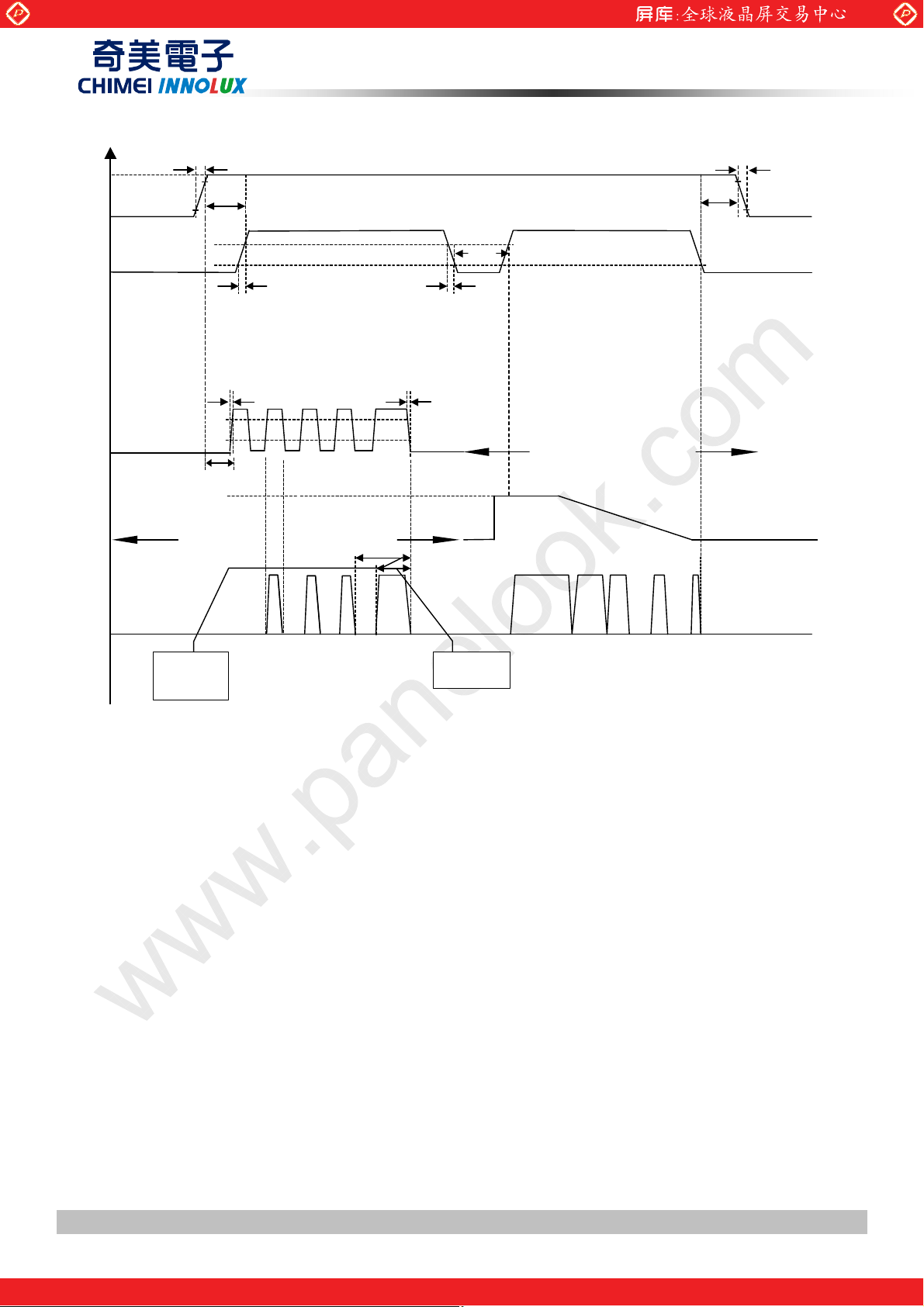
6.2 POWER ON/OFF SEQUENCE
(Ta = 25 ± 2 ºC)
To prevent a latch-up or DC operation of LCD module, the power on/off sequence should be as the diagram
below.
0V
0.5ЉЉЉЉT1ЉЉЉЉ10ms
2
0ЉЉЉЉT
0ЉЉЉЉT
500ms ЉЉЉЉT
LVDS Signals
ЉЉЉЉ50ms
3
ЉЉЉЉ50ms
4
0V
www.panelook.com
PRODUCT SPECIFICATION
0.1V
CC
T
1
T
2
Power On
VA L I D
0.1V
cc
T
3
T
4
0ЉЉЉЉT7ЉЉЉЉT
0ЉЉЉЉT8ЉЉЉЉT
2
3
T
7
T
8
Option Signals
(SELLVDS,…)
Backlight (Recommended)
ЉЉЉЉ
5
T
6
1500msЉЉЉЉT
100ms
50%
T
5
Power ON/OFF Sequence
Note (1) The supply voltage of the external system for the module input should follow the definition of Vcc.
Note (2) Apply the lamp voltage within the LCD operation range. When the backlight turns on before the LCD
operation or the LCD turns off before the backlight turns off, the display may momentarily become
50%
6
T
abnormal screen.
Note (3) In case of Vcc is in off level, please keep the level of input signals on the low or high impedance. If
T2<0,that maybe cause electrical overstress failure.
Note (4) T4 should be measured after the module has been fully discharged between power off and on period.
Note (5) Interface signal shall not be kept at high impedance when the power is on.
Version 2.0 28 DateΚΚΚΚ27 May 2010
The copyright belongs to CHIMEI InnoLux. Any unauthorized use is prohibited
One step solution for LCD / PDP / OLED panel application: Datasheet, inventory and accessory!
www.panelook.com
Page 29

Global LCD Panel Exchange Center
7. OPTICAL CHARACTERISTICS
7.1 TEST CONDITIONS
Item Symbol Value Unit
www.panelook.com
PRODUCT SPECIFICATION
Ambient Temperature Ta
Ambient Humidity Ha
Supply Voltage VCC 12 V
Input Signal According to typical value in "3. ELECTRICAL CHARACTERISTICS"
LED Current IL 120 mA
Vertical Frame Rate Fr 60 Hz
The LCD module should be stabilized at given temperature for 1 hour to avoid abrupt temperature change during
measuring. In order to stabilize the luminance, the measurement should be executed after lighting backlight for 1
hour in a windless room.
25±2
50±10
oC
%RH
Version 2.0 29 DateΚΚΚΚ27 May 2010
The copyright belongs to CHIMEI InnoLux. Any unauthorized use is prohibited
One step solution for LCD / PDP / OLED panel application: Datasheet, inventory and accessory!
www.panelook.com
Page 30

Global LCD Panel Exchange Center
7.2 OPTICAL SPECIFICATIONS
The relative measurement methods of optical characteristics are shown in 7.2. The following items should be
measured under the test conditions described in 7.1 and stable environment shown in 7.1.
Item Symbol Condition Min. Typ. Max. Unit Note
www.panelook.com
PRODUCT SPECIFICATION
Contrast Ratio
Response Time
Center Luminance of
White
White Variation
Cross Talk
Red
Green
Color
Chromaticit
y
Blue
White
CR 4200 6000 - - Note (2)
Gray to
gray
LC 350 450 - cd/m2Note (4)
δW
CT - - 4 % Note (5)
Rx 0.637 -
Ry 0.325 -
Gx 0.316 -
Gy 0.637 -
Bx 0.152 -
By 0.051 -
Wx 0.280 -
Wy
θx=0°, θy =0°
Viewing angle
at normal direction
- 5.5 10 ms Note (3)
- - 1.3 - Note (6)
Typ. –
0.03
0.290
Typ+
0.03
-
-
Color Gamut
C.G
θx+
72 - % NTSC
80 88 -
Horizontal
Viewing
Angle
θx-
CR≥20
θY+
80 88 -
Deg. Note (1)
80 88 -
Vertical
θY-
Note (1) Definition of Viewing Angle (θx, θy):
Viewing angles are measured by Autronic Conoscope Cono-80.
80 88 -
Version 2.0 30 DateΚΚΚΚ27 May 2010
The copyright belongs to CHIMEI InnoLux. Any unauthorized use is prohibited
One step solution for LCD / PDP / OLED panel application: Datasheet, inventory and accessory!
www.panelook.com
Page 31

Global LCD Panel Exchange Center
www.panelook.com
PRODUCT SPECIFICATION
Note (2) Definition of Contrast Ratio (CR):
The contrast ratio can be calculated by the following expression.
Contrast Ratio (CR) =
CR = CR (5), where CR (X) is corresponding to the Contrast Ratio of the point X at the figure in Note (6).
Note (3) Definition of Gray-to-Gray Switching Time:
pixels whiteall withLuminance Surface
pixels black all withLuminance Surface
The driving signal means the signal of gray level 0, 252, 508, 764, and 1023.
Gray to gray average time means the average switching time of gray level 0, 252, 508, 764, and 1023.
to each other.
Note (4) Definition of Luminance of White (L
Measure the luminance of gray level 1023. at center point and 5 points
L
= L (5), where L (X) is corresponding to the luminance of the point X at the figure in Note (6).
C
):
C
Version 2.0 31 DateΚΚΚΚ27 May 2010
The copyright belongs to CHIMEI InnoLux. Any unauthorized use is prohibited
One step solution for LCD / PDP / OLED panel application: Datasheet, inventory and accessory!
www.panelook.com
Page 32

Global LCD Panel Exchange Center
www.panelook.com
PRODUCT SPECIFICATION
ʳʳʳʳʳʳ
Note (5) Definition of Cross Talk (CT):
CT = | YB – YA | / YA
Where:
YA = Luminance of measured location without gray level 0 pattern (cd/m2)
YB = Luminance of measured location with gray level 0 pattern (cd/m2)
×
100 (%)
Note (6) Definition of White Variation (δW):
Measure the luminance of gray level 1023 at 5 points
δ
W = Maximum [L (1), L (2), L (3), L (4), L (5)] / Minimum [L (1), L (2), L (3), L (4), L (5)]
D
4
1 2
W
4
W
2
3 4
3W
4
Horizontal Line
D
D
2
5
3D
4
X
Test point :
X = 1 ~ 5
Version 2.0 32 DateΚΚΚΚ27 May 2010
The copyright belongs to CHIMEI InnoLux. Any unauthorized use is prohibited
One step solution for LCD / PDP / OLED panel application: Datasheet, inventory and accessory!
www.panelook.com
Page 33

Global LCD Panel Exchange Center
8. DEFINITION OF LABELS
8.1 CMO MODULE LABEL
The barcode nameplate is pasted on each module as illustration, and its definitions are as following explanation.
www.panelook.com
PRODUCT SPECIFICATION
CHI MEI
OPTOELECTRONICS
V420H2 –LE4 Rev. XX
X X X X X X X Y M D L N N N N
(a) Model Name: V420H2-LE4
(b) Revision: Rev. XX, for example: A0, A1… B1, B2… or C1, C2…etc.
(c) Serial ID: X X
X X X X X Y M D L N N N N
Serial No.
E207943
MAD E IN TAIWAN
GEMN
Product Line
Year, Month, Date
CMO Internal Use
CMO Internal Use
Serial ID includes the information as below:
(a) Manufactured Date: Year: 2001=1, 2002=2, 2003=3, 2004=4….2010=0, 2011=1, 2012=2....
Month: 1~9, A~C, for Jan. ~ Dec.
Day: 1~9, A~Y, for 1
(b) Revision Code: Cover all the change
(c) Serial No.: Manufacturing sequence of product
Revision
CMO Internal Use
st
to 31st, exclude I ,O, and U.
Version 2.0 33 DateΚΚΚΚ27 May 2010
The copyright belongs to CHIMEI InnoLux. Any unauthorized use is prohibited
One step solution for LCD / PDP / OLED panel application: Datasheet, inventory and accessory!
www.panelook.com
Page 34

Global LCD Panel Exchange Center
(d) Product Line: 1 -> Line1, 2 -> Line 2, …etc.
www.panelook.com
PRODUCT SPECIFICATION
Version 2.0 34 DateΚΚΚΚ27 May 2010
The copyright belongs to CHIMEI InnoLux. Any unauthorized use is prohibited
One step solution for LCD / PDP / OLED panel application: Datasheet, inventory and accessory!
www.panelook.com
Page 35

Global LCD Panel Exchange Center
9. PACKAGING
9.1 PACKING SPECIFICATIONS
(1) 5 LCD TV modules / 1 Box
(2) Box dimensions : 1085(L)x296(W)x653(H)mm
(3) Weight : Approx. 44 Kg(5 modules per carton)
9.2 PACKING METHOD
Figures 9-1 and 9-2 are the packing method
www.panelook.com
PRODUCT SPECIFICATION
Figure.9-1 packing method
Version 2.0 35 DateΚΚΚΚ27 May 2010
The copyright belongs to CHIMEI InnoLux. Any unauthorized use is prohibited
One step solution for LCD / PDP / OLED panel application: Datasheet, inventory and accessory!
www.panelook.com
Page 36

Global LCD Panel Exchange Center
(40ft Container)
www.panelook.com
PRODUCT SPECIFICATION
Air TransportationSea / Land Transportation
Figure.9-2 packing method
Version 2.0 36 DateΚΚΚΚ27 May 2010
The copyright belongs to CHIMEI InnoLux. Any unauthorized use is prohibited
One step solution for LCD / PDP / OLED panel application: Datasheet, inventory and accessory!
www.panelook.com
Page 37

Global LCD Panel Exchange Center
www.panelook.com
PRODUCT SPECIFICATION
10. PRECAUTIONS
10.1 ASSEMBLY AND HANDLING PRECAUTIONS
(1) Do not apply rough force such as bending or twisting to the module during assembly.
(2) It is recommended to assemble or to install a module into the user’s system in clean working areas. The
dust and oil may cause electrical short or worsen the polarizer.
(3) Do not apply pressure or impulse to the module to prevent the damage of LCD panel and backlight.
(4) Always follow the correct power-on sequence when the LCD module is turned on. This can prevent the
damage and latch-up of the CMOS LSI chips.
(5) Do not plug in or pull out the I/F connector while the module is in operation.
(6) Do not disassemble the module.
(7) Use a soft dry cloth without chemicals for cleaning, because the surface of polarizer is very soft and
easily scratched.
(8) Moisture can easily penetrate into LCD module and may cause the damage during operation.
(9) High temperature or humidity may deteriorate the performance of LCD module. Please store LCD
modules in the specified storage conditions.
(10) When ambient temperature is lower than 10ºC, the display quality might be reduced. For example, the
response time will become slow, and the starting voltage of LED light bar will be higher than that of room
temperature.
10.2 SAFETY PRECAUTIONS
(1) The startup voltage of a backlight is over 1000 Volts. It may cause an electrical shock while assembling
with the converter. Do not disassemble the module or insert anything into the backlight unit.
(2) If the liquid crystal material leaks from the panel, it should be kept away from the eyes or mouth. In case
of contact with hands, skin or clothes, it has to be washed away thoroughly with soap.
(3) After the module’s end of life, it is not harmful in case of normal operation and storage.
Version 2.0 37 DateΚΚΚΚ27 May 2010
The copyright belongs to CHIMEI InnoLux. Any unauthorized use is prohibited
One step solution for LCD / PDP / OLED panel application: Datasheet, inventory and accessory!
www.panelook.com
Page 38

Global LCD Panel Exchange Center
11. MECHANICAL CHARACTERISTICS
www.panelook.com
PRODUCT SPECIFICATION
ڻႝηިҽԖϦљ
ΓΓΓΓΓΓΓΓΓΓΓΓΓΓΓΓΓΓΓΓΓΓΓΓΓΓΓΓ
Version 2.0 38 DateΚΚΚΚ27 May 2010
The copyright belongs to CHIMEI InnoLux. Any unauthorized use is prohibited
One step solution for LCD / PDP / OLED panel application: Datasheet, inventory and accessory!
www.panelook.com
Page 39

Global LCD Panel Exchange Center
www.panelook.com
PRODUCT SPECIFICATION
ڻႝηިҽԖϦљ
CHI MEI
Version 2.0 39 DateΚΚΚΚ27 May 2010
The copyright belongs to CHIMEI InnoLux. Any unauthorized use is prohibited
One step solution for LCD / PDP / OLED panel application: Datasheet, inventory and accessory!
www.panelook.com
Page 40
Global LCD Panel Exchange Center
Appendix – TWO Wire BUS INTRODUCTION
A.1 PIN ASSIGNMENT
51pins LVDS connector
Pin8: SCL
Pin9: SDA
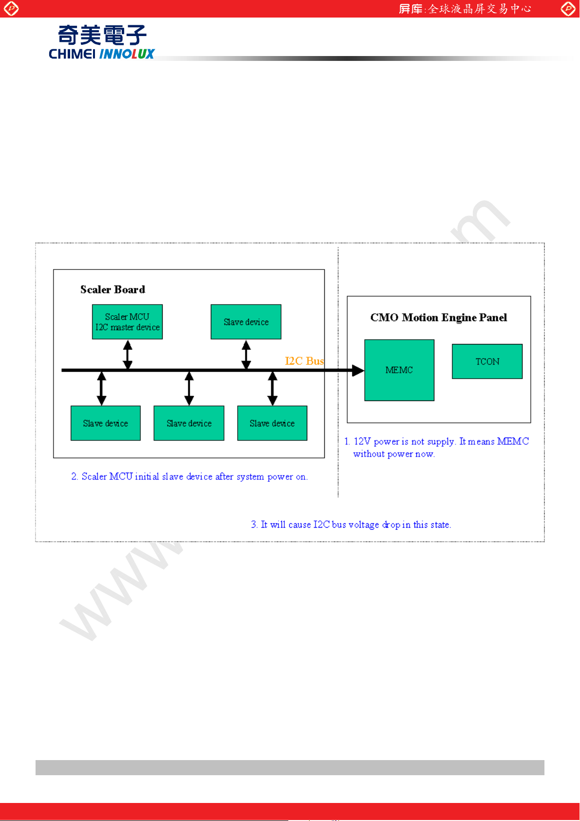
A.2 I2C BUS APPLICATION NOTE
I2C bus: (The I2C bus must for MEMC only or prevent the I2C bus voltage drop down in initial state)
www.panelook.com
PRODUCT SPECIFICATION
Version 2.0 40 DateΚΚΚΚ27 May 2010
The copyright belongs to CHIMEI InnoLux. Any unauthorized use is prohibited
One step solution for LCD / PDP / OLED panel application: Datasheet, inventory and accessory!
www.panelook.com
Page 41

Global LCD Panel Exchange Center
A.3 TWO WIRE BUS DEVICE ADDRESS
Two wire device address: default is 0x40, 1 byte
Two wire command: the range is 0x00 to 0xFF, 1 byte, see the two wire command table.
Two wire bus format:
www.panelook.com
PRODUCT SPECIFICATION
A.4 TWO WAY TO CONTROL THE TWO WIRE BUS
There are two options to control the two wires bus command.
Two wire bus 6 bytes format
Two wire bus 3 bytes format
Version 2.0 41 DateΚΚΚΚ27 May 2010
The copyright belongs to CHIMEI InnoLux. Any unauthorized use is prohibited
One step solution for LCD / PDP / OLED panel application: Datasheet, inventory and accessory!
www.panelook.com
Page 42

Global LCD Panel Exchange Center
www.panelook.com
PRODUCT SPECIFICATION
Note:
A transmission basically consists of a START condition, a SLA+R/W, one or more data packets and a STOP
condition. An empty message, consisting of a START followed by a STOP condition, is illegal. Note that the
wired-ANDing of the SCL line can be used to implement handshaking between the master and the slave. The slave can
extend the SCL low period by pulling the SCL line low. This is useful if the clock speed set up by the master is too fast
for the slave, or the slave needs extra time for processing between the data transmissions. The slave extending the
SCL low period will not affect the SCL high period, which is determined by the master. As a consequence, the slave can
reduce the TWI data transfer speed by prolonging the SCL duty cycle.
Version 2.0 42 DateΚΚΚΚ27 May 2010
The copyright belongs to CHIMEI InnoLux. Any unauthorized use is prohibited
One step solution for LCD / PDP / OLED panel application: Datasheet, inventory and accessory!
www.panelook.com
Page 43

Global LCD Panel Exchange Center
A.5 TWO WIRE BUS COMMAND TABLE
There is two wire bus command table.
Command Name
All OSD Protection 0x00 R/W OSDx Enable Flag Contorl
OSD1_Start_Protection 0x01 R/W OSD1 Protection Start Position
OSD2_Start_Protection 0x02 R/W OSD2 Protection Start Position
OSD3_Start_Protection 0x03 R/W OSD3 Protection Start Position
OSD4_Start_Protection 0x04 R/W OSD4 Protection Start Position
OSD1_End_Protection 0x05 R/W OSD1 Protection End Position
OSD2_End_Protection 0x06 R/W OSD2 Protection End Position
www.panelook.com
PRODUCT SPECIFICATION
Access
Mode Description
OSD3_End_Protection 0x07 R/W OSD3 Protection End Position
OSD4_End_Protection 0x08 R/W OSD4 Protection End Position
Demo Window 0x09 R/W ME Performance Demo
MEMC Level 0x0A R/W ME Performance
GV Mode 0x0B R/W ME Operation
Blanking 0x0C R/W Blinking the screen
RPF 0x0D R/W Rotation picture function
Version 2.0 43 DateΚΚΚΚ27 May 2010
The copyright belongs to CHIMEI InnoLux. Any unauthorized use is prohibited
One step solution for LCD / PDP / OLED panel application: Datasheet, inventory and accessory!
www.panelook.com
Page 44

Global LCD Panel Exchange Center
Enable All OSD Protection
www.panelook.com
PRODUCT SPECIFICATION
OSD # 1~4 Start Protection
OSD # 1~4 End Protection
Version 2.0 44 DateΚΚΚΚ27 May 2010
The copyright belongs to CHIMEI InnoLux. Any unauthorized use is prohibited
One step solution for LCD / PDP / OLED panel application: Datasheet, inventory and accessory!
www.panelook.com
Page 45

Global LCD Panel Exchange Center
Demo Window
www.panelook.com
PRODUCT SPECIFICATION
MEMC Level
Version 2.0 45 DateΚΚΚΚ27 May 2010
The copyright belongs to CHIMEI InnoLux. Any unauthorized use is prohibited
One step solution for LCD / PDP / OLED panel application: Datasheet, inventory and accessory!
www.panelook.com
Page 46

Global LCD Panel Exchange Center
GV Mode
www.panelook.com
PRODUCT SPECIFICATION
Blanking (Enable/Disable)
Rotation Panel Function
Version 2.0 46 DateΚΚΚΚ27 May 2010
The copyright belongs to CHIMEI InnoLux. Any unauthorized use is prohibited
One step solution for LCD / PDP / OLED panel application: Datasheet, inventory and accessory!
www.panelook.com
Page 47

Global LCD Panel Exchange Center
A.6 TWO WIRE BUS REQUIREMENT
Sy mbol Parame te r Co nditio n M in M ax Unit
V
V
t
r
t
cf
I
i
C
f
SCL
R
t
HDSTA
t
LOW
t
HIGH
t
SUST A
t
HDDAT
t
SUDAT
t
SUST O
t
QLF
Input Low-voltage
L
Inp ut High- vo lta ge
H
Rise Time for both SDA and SCL 20 + 0.1C
Output Fall Time from V
IHmin
Input Current each I/O Pin 0.1VCC < Vi < 0.9V
Capacitance for each I/O Pin NA
i
SCL Clock Frequency
Value of Pull-up resistor f
P
Hold Time (repeated) STAR Condition f
Low Period of the SCL Clock f
High Period of the SCL Clock f
Set-up time for a repeated STAR Condition f
Data hold time f
Data setup time f
Setup time for STOP Condition f
Bus free time between a STOP and START Condition f
to V
www.panelook.com
PRODUCT SPECIFICATION
ILmax
˃˃ˁˊ
˅ˁˊ ˆˁˆ
10 pF < Cb < 400 pF 20 + 0.1C
CC
ˀ˄˃ ˄˃
ˇˈ˃
50KHz
SC L
SC L
SC L
SC L
SC L
SC L
SC L
SC L
SC L
Љ
50KHz
Љ
50KHz
Љ
50KHz
Љ
50KHz
Љ
50KHz
Љ
50KHz
Љ
50KHz
Љ
50KHz
Љ
ˆ˃˃˃
ˇ
ˇˁˊ
ˇ
ˇˁˊ
˃ˆˁˇˈ
˅ˈ˃
ˇ
ˇˁˊ
ˆ˃˃
b
˅ˈ˃
b
˄˃
1000ns/C
NA us
NA us
NA us
NA us
NA ns
NA us
NA us
V
V
ns
ns
uA
pF
KHz
Ө
b
us
Version 2.0 47 DateΚΚΚΚ27 May 2010
The copyright belongs to CHIMEI InnoLux. Any unauthorized use is prohibited
One step solution for LCD / PDP / OLED panel application: Datasheet, inventory and accessory!
www.panelook.com
Page 48

Global LCD Panel Exchange Center
A.7 THE TWO WIRE BUS SEQUENCE
I. Initial state
www.panelook.com
PRODUCT SPECIFICATION
II. Stable state
Version 2.0 48 DateΚΚΚΚ27 May 2010
The copyright belongs to CHIMEI InnoLux. Any unauthorized use is prohibited
One step solution for LCD / PDP / OLED panel application: Datasheet, inventory and accessory!
www.panelook.com
 Loading...