

Page 1
Global LCD Panel Exchange Center
MODEL NO.: V400H1
www.panelook.com
PRODUCT SPECIFICATION
□ Tentative Specification
□ Preliminary Specification
■ Approval Specification
SUFFIX: LHA
Customer:
APPROVED BY SIGNATURE
Name / Title
Note
Please return 1 copy for your confirmation with your
signature and comments.
Approved By Checked By Prepared By
Chao-Chun Chung Josh Chi Joanne Chung
Version 2.0 1 DateΚΚΚΚ03 Mar 2011
The copyright belongs to CHIMEI InnoLux. Any unauthorized use is prohibited
One step solution for LCD / PDP / OLED panel application: Datasheet, inventory and accessory!
www.panelook.com
Page 2
Global LCD Panel Exchange Center
www.panelook.com
PRODUCT SPECIFICATION
CONTENTS
1. GENERAL DESCRIPTION ......................................................................................................................................................... 5
1.1 OVERVIEW ..........................................................................................................................................................5
1.2 FEATURES ..........................................................................................................................................................5
1.3 APPLICATION...................................................................................................................................................... 5
1.4 GENERAL SPECIFICATIONS .............................................................................................................................5
1.5 MECHANICAL SPECIFICATIONS....................................................................................................................... 6
2. ABSOLUTE MAXIMUM RATINGS .......................................................................................................................................... 7
2.1 ABSOLUTE RATINGS OF ENVIRONMENT ........................................................................................................ 7
2.2 PACKAGE STORAGE.......................................................................................................................................... 8
2.3 ELECTRICAL ABSOLUTE RATINGS .................................................................................................................. 8
2.3.1 TFT LCD MODULE ....................................................................................................................................8
2.3.2 BACKLIGHT BALANCE BOARD UNIT...................................................................................................... 8
3. ELECTRICAL CHARACTERISTICS ......................................................................................................................................... 9
3.1 TFT LCD MODULE ..............................................................................................................................................9
3.2 BACKLIGHT CONNECTOR PIN CONFIGURATION......................................................................................... 12
3.2.1 LAMP SPECIFICATION (Ta = 25 ± 2 ºC) ............................................................................................12
3.2.2 ELECTRICAL SPECIFICATION...............................................................................................................12
4.1 TFT LCD MODULE ............................................................................................................................................15
5. INPUT TERMINAL PIN ASSIGNMENT................................................................................................................................ 16
5.1 TFT LCD Module Input....................................................................................................................................... 16
5.2 BACKLIGHT UNIT.............................................................................................................................................. 19
5.3 BALANCE BOARD UNIT ...................................................................................................................................20
5.4 BLOCK DIAGRAM OF INTERFACE.................................................................................................................. 21
5.5 LVDS INTERFACE ............................................................................................................................................. 23
5.6 COLOR DATA INPUT ASSIGNMENT ................................................................................................................ 24
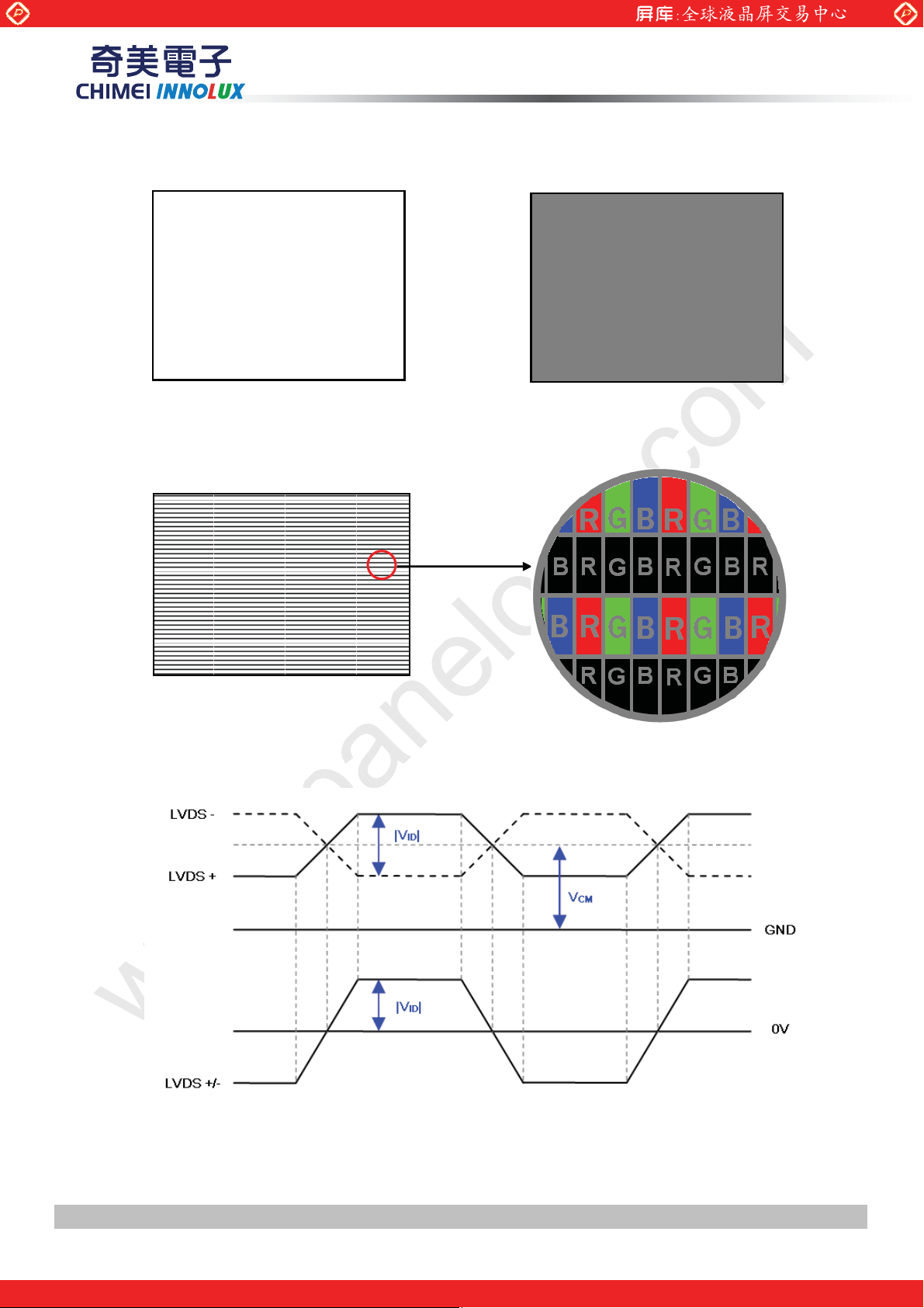
The brightness of each primary color (red, green and blue) is based on the 10-bit gray scale data input for the
color. The higher the binary input, the brighter the color. The table below provides the assignment of the color
versus data input. .....................................................................................................................................................24
6. INTERFACE TIMING................................................................................................................................................................ 25
6.1 INPUT SIGNAL TIMING SPECIFICATIONS...................................................................................................... 25
7. OPTICAL CHARACTERISTICS............................................................................................................................................... 29
7.1 TEST CONDITIONS...........................................................................................................................................29
Version 2.0 2 DateΚΚΚΚ03 Mar 2011
The copyright belongs to CHIMEI InnoLux. Any unauthorized use is prohibited
One step solution for LCD / PDP / OLED panel application: Datasheet, inventory and accessory!
www.panelook.com
Page 3

Global LCD Panel Exchange Center
www.panelook.com
PRODUCT SPECIFICATION
7.2 OPTICAL SPECIFICATIONS .............................................................................................................................30
PRECAUTIONS.............................................................................................................................................................................. 35
8.1 ASSEMBLY AND HANDLING PRECAUTIONS .................................................................................................35
8.2 SAFETY PRECAUTIONS ..................................................................................................................................35
9. DEFINITION OF LABELS......................................................................................................................................................... 36
9.1 CMI MODULE LABEL ........................................................................................................................................36
10. PACKAGING............................................................................................................................................................................ 37
10.1 PACKAGING SPECIFICATIONS ..................................................................................................................... 37
10.2 PACKAGING METHOD.................................................................................................................................... 38
11. MECHANICAL CHARACTERISTIC .................................................................................................................................... 40
Appendix – TWO Wire BUS INTRODUCTION ........................................................................................................................ 43
A.1 PIN ASSIGNMENT ............................................................................................................................................ 43
A.2 I2C BUS APPLICATION NOTE ......................................................................................................................... 43
A.3 TWO WIRE BUS DEVICE ADDRESS ...............................................................................................................43
Version 2.0 3 DateΚΚΚΚ03 Mar 2011
The copyright belongs to CHIMEI InnoLux. Any unauthorized use is prohibited
One step solution for LCD / PDP / OLED panel application: Datasheet, inventory and accessory!
www.panelook.com
Page 4
Global LCD Panel Exchange Center
Version Date Page(New) Section Description
Ver. 2.0 Mar. 03, 2011 All All The approval specification was first issued.
www.panelook.com
PRODUCT SPECIFICATION
REVISION HISTORY
Version 2.0 4 DateΚΚΚΚ03 Mar 2011
The copyright belongs to CHIMEI InnoLux. Any unauthorized use is prohibited
One step solution for LCD / PDP / OLED panel application: Datasheet, inventory and accessory!
www.panelook.com
Page 5
Global LCD Panel Exchange Center
1. GENERAL DESCRIPTION
1.1 OVERVIEW
V400H1-LHA is a 40” TFT Liquid Crystal Display module with 12-CCFL Backlight unit and 4ch-LVDS interface.
This module supports 1920 x 1080 Full HDTV format and can display true 1.07G (8-bit+Hi-FRC) colors. The
balance board module for backlight is built-in.
1.2 FEATURES
Ё High brightness (500 nits)
Ё High contrast ratio (6000:1)
Ё Fast response time (Gray to gray average 5.5 ms)
Ё High color saturation (NTSC 72%)
Ё Full HDTV (1920 x 1080 pixels) resolution, true HDTV format
Ё DE (Data Enable) only mode
www.panelook.com
PRODUCT SPECIFICATION
Ё LVDS (Low Voltage Differential Signaling) interface
Ё Optimized response time for 120 Hz frame rate
Ё Ultra wide viewing angle : Super MVA technology
Ё Viewing Angle : 160(H)/150(V) (CR>10) TN Technology
Ё RoHs compliance
1.3 APPLICATION
Ё Standard Living Room TVs
Ё Public Display Application
Ё Home Theater Application
Ё MFM Application
1.4 GENERAL SPECIFICATIONS
Item Specification Unit Note
Active Area 885.6(H) x 498.15 (V) (40” diagonal) mm
Bezel Opening Area 891.7 (H) x 504.8 (V) mm
Driver Element a-si TFT active matrix - -
Pixel Number 1920 x R.G.B. x 1080 pixel -
(1)
Pixel Pitch(Sub Pixel) 0.15375 (H) x 0.46125 (V) mm -
Pixel Arrangement RGB vertical stripe - -
Display Colors 1.07G color -
Display Operation Mode Transmissive mode / Normally Black - -
Surface Treatment Anti-Glare coating (Haze 11%) - (2)
Note (1) Please refer to the attached drawings in chapter 9 for more information about the front and back outlines.
Note (2) The spec. of the surface treatment is temporarily for this phase. CMI reserves the rights to change this feature.
Version 2.0 5 DateΚΚΚΚ03 Mar 2011
The copyright belongs to CHIMEI InnoLux. Any unauthorized use is prohibited
One step solution for LCD / PDP / OLED panel application: Datasheet, inventory and accessory!
www.panelook.com
Page 6
Global LCD Panel Exchange Center
1.5 MECHANICAL SPECIFICATIONS
Item Min. Typ. Max. Unit Note
Horizontal (H) 951 952 953 mm (1)
www.panelook.com
PRODUCT SPECIFICATION
Module Size
Weight - 9439.5 - g -
Note (1) Please refer to the attached drawings for more information of front and back outline dimensions.
Note (2) Module Depth is between bezel to T-CON cover.
Note (3) Module Depth is between bezel to Balance board cover.
Vertical (V) 550 551 552 mm (1)
Depth (D) 49 50 51 mm (2)
Depth (D) 56.3 57.3 58.3 mm (3)
Version 2.0 6 DateΚΚΚΚ03 Mar 2011
The copyright belongs to CHIMEI InnoLux. Any unauthorized use is prohibited
One step solution for LCD / PDP / OLED panel application: Datasheet, inventory and accessory!
www.panelook.com
Page 7
Global LCD Panel Exchange Center
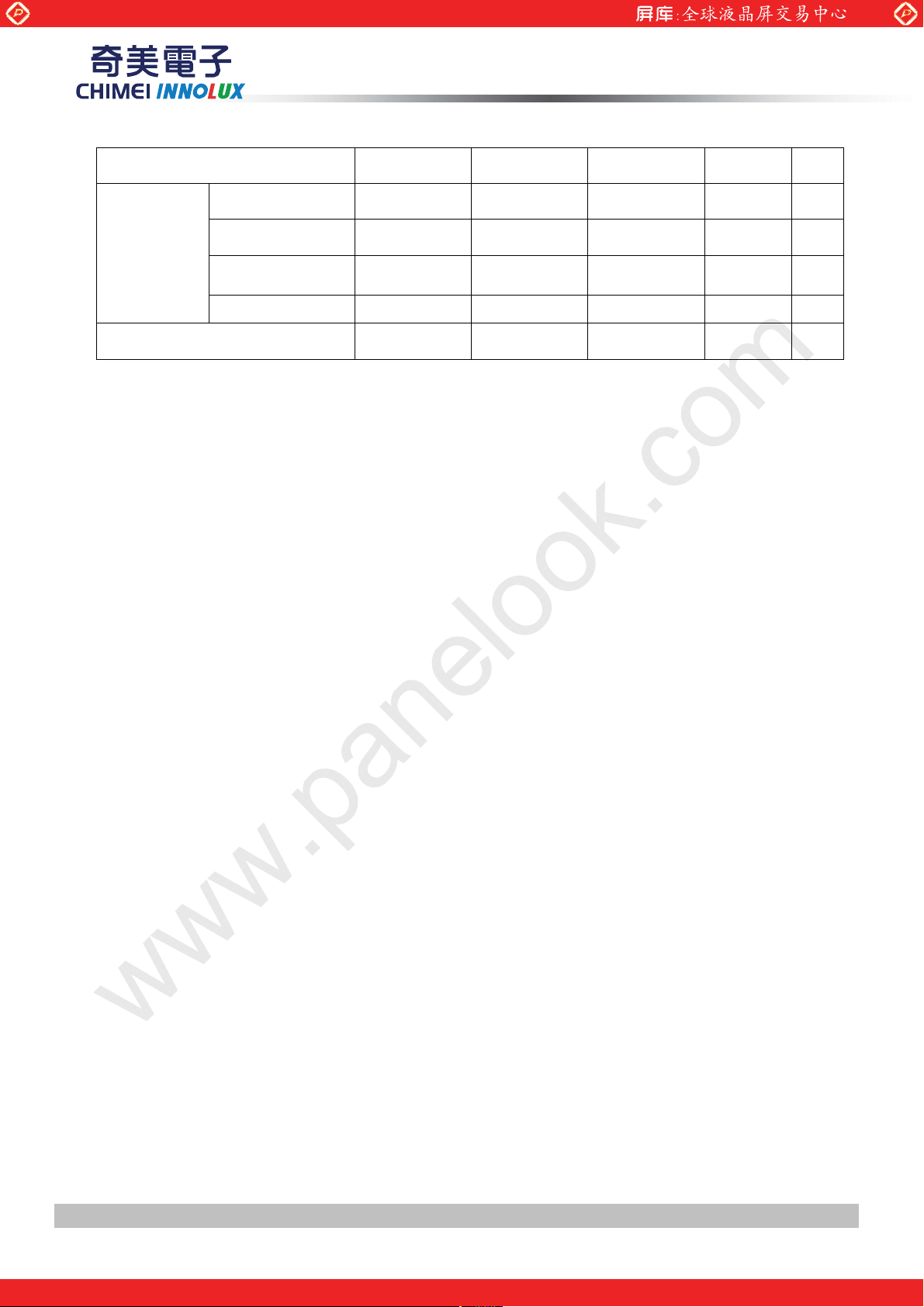
2. ABSOLUTE MAXIMUM RATINGS
2.1 ABSOLUTE RATINGS OF ENVIRONMENT
Item Symbol
Storage Temperature TST -20 +60 ºC (1)
Operating Ambient Temperature TOP 0 50 ºC (1), (2)
Shock (Non-Operating) SNOP - 50 G (3), (5)
Vibration (Non-Operating) VNOP - 1.0 G (4), (5)
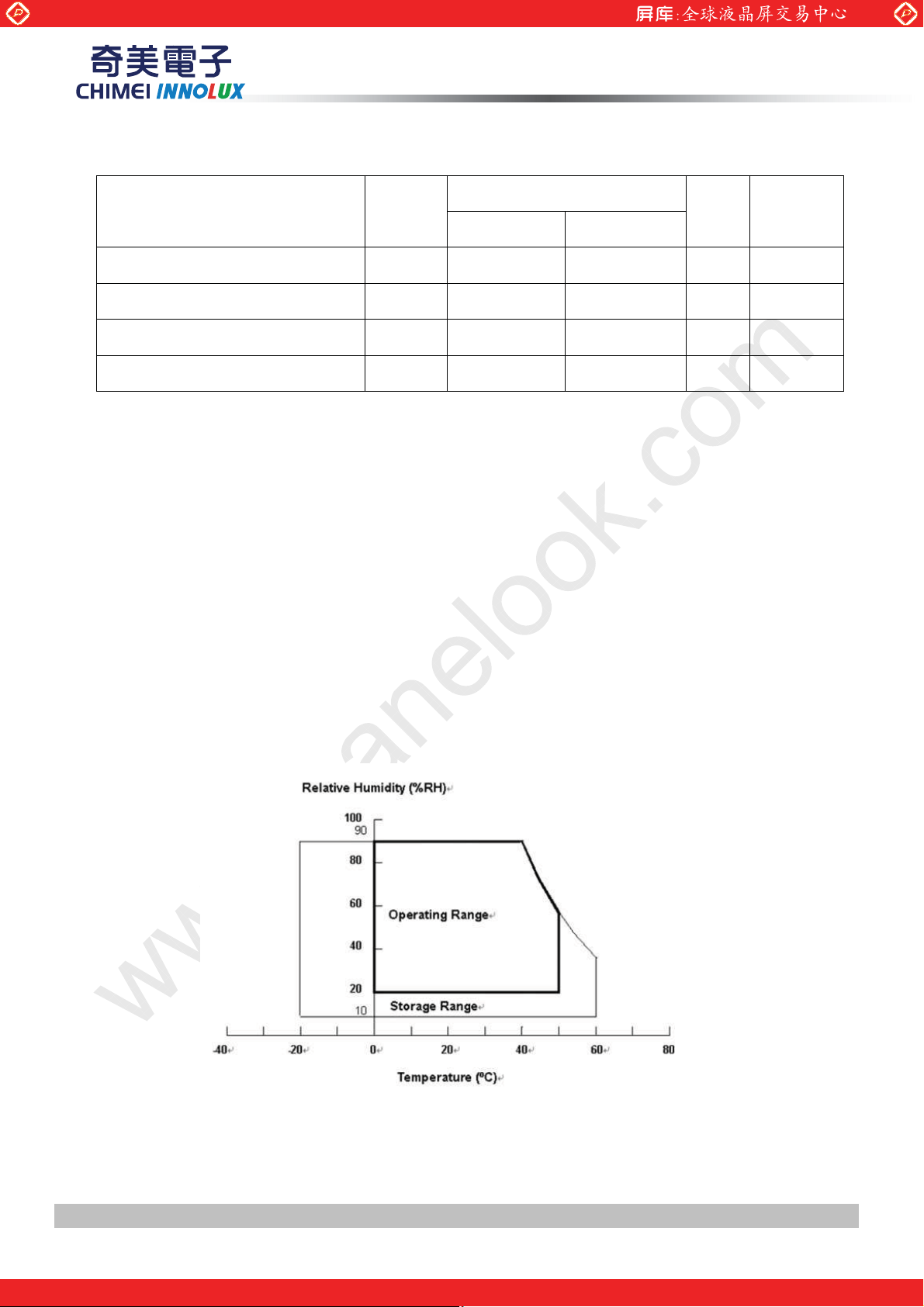
Note (1) Temperature and relative humidity range is shown in the figure below.
(a) 90 %RH Max. (Ta Љ 40 ºC).
(b) Wet-bulb temperature should be 39 ºC Max. (Ta > 40 ºC).
www.panelook.com
PRODUCT SPECIFICATION
Value
Unit Note
Min. Max.
(c) No condensation.
Note (2) The maximum operating temperature is based on the test condition that the surface temperature of
display area is less than or equal to 65 ºC with LCD module alone in a temperature controlled chamber.
Thermal management should be considered in final product design to prevent the surface temperature
of display area from being over 65 ºC. The range of operating temperature may degrade in case of
improper thermal management in final product design.
Note (3) 11 ms, half sine wave, 1 time for ± X, ± Y, ± Z.
Note (4) 10 ~ 200 Hz, 10 min, 1 time each X, Y, Z.
Note (5) At testing Vibration and Shock, the fixture in holding the module has to be hard and rigid enough so that
the module would not be twisted or bent by the fixture.
Version 2.0 7 DateΚΚΚΚ03 Mar 2011
The copyright belongs to CHIMEI InnoLux. Any unauthorized use is prohibited
One step solution for LCD / PDP / OLED panel application: Datasheet, inventory and accessory!
www.panelook.com
Page 8
Global LCD Panel Exchange Center
2.2 PACKAGE STORAGE
When storing modules as spares for a long time, the following precaution is necessary.
(a) Do not leave the module in high temperature, and high humidity for a long time, It is highly recommended to
store the module with temperature from 0 to 35 к at normal humidity without condensation.
(b) The module shall be stored in dark place. Do not store the TFT-LCD module in direct sunlight or fluorescent
light.
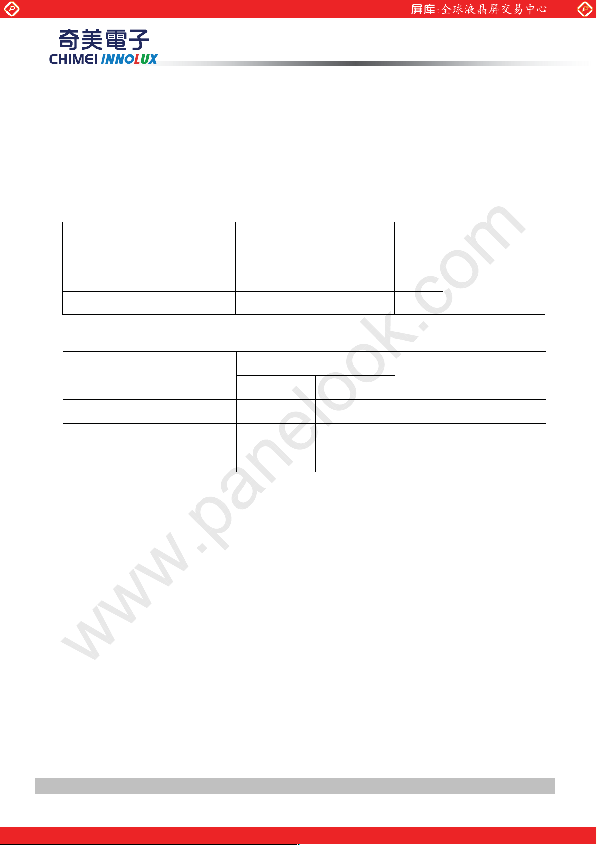
2.3 ELECTRICAL ABSOLUTE RATINGS
2.3.1 TFT LCD MODULE
Item Symbol
Power Supply Voltage VCC -0.3 13.5 V
Logic Input Voltage VIN -0.3 3.6 V
www.panelook.com
PRODUCT SPECIFICATION
Value
Unit Note
Min. Max.
(1)
2.3.2 BACKLIGHT BALANCE BOARD UNIT
Value
Item Symbol
Min. Max.
Lamp Voltage V
IP Board Supply Voltage High / Low 195 (Low) 390 (High) Vrms
Control Signal Level
Note (1) Permanent damage to the device may occur if maximum values are exceeded. Function operation
should be restricted to the conditions described under Normal Operating Conditions.
Note (2) No moisture condensation or freezing.
Note (3) The control signals include On/Off Control and Internal PWM Control.
Ё
Ё
-0.3 15 V Control Signal Level
3000 VRMS Lamp Voltage
Unit Note
IP Board Supply
Voltage
Version 2.0 8 DateΚΚΚΚ03 Mar 2011
The copyright belongs to CHIMEI InnoLux. Any unauthorized use is prohibited
One step solution for LCD / PDP / OLED panel application: Datasheet, inventory and accessory!
www.panelook.com
Page 9
Global LCD Panel Exchange Center
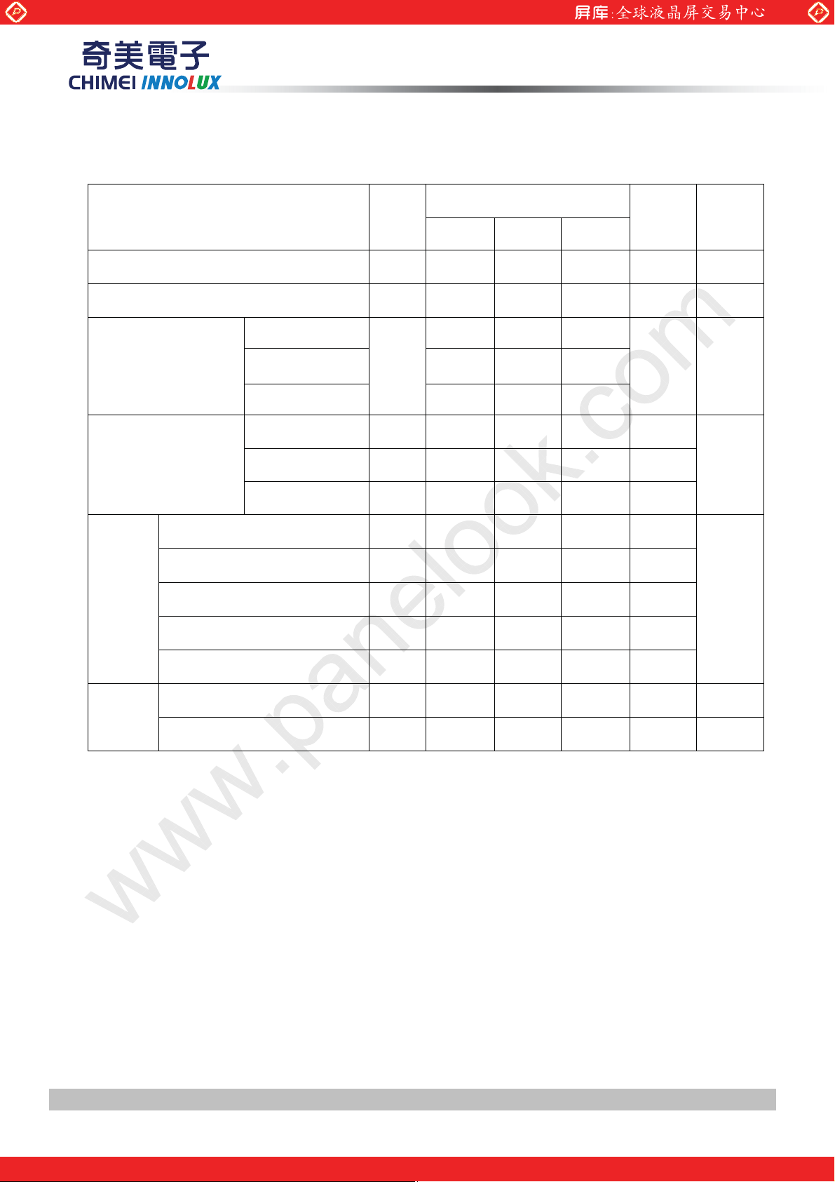
3. ELECTRICAL CHARACTERISTICS
3.1 TFT LCD MODULE
(Ta = 25 ± 2 ºC)
Parameter Symbol
Power Supply Voltage VCC 10.8 12 13.2 V (1)
www.panelook.com
PRODUCT SPECIFICATION
Value
Unit Note
Min. Typ. Max.
Rush Current I
White Pattern
Power consumption
Black Pattern
Horizontal Stripe
White Pattern
Power Supply Current
Black Pattern
Horizontal Stripe
Differential Input High
Threshold Voltage
Differential Input Low
Threshold Voltage
LVDS
interface
Common Input Voltage VCM 1.0 1.2 1.4 V
Differential input voltage
(single-end)
Terminating Resistor R
CMIS
interface
Input High Threshold Voltage VIH 2.7
Input Low Threshold Voltage V
RUSH
ЁЁ
Ё
P
T
Ё
Ё
ЁЁ
ЁЁ
ЁЁ
V
V
|V
LVT H
LVT L
ID
T
IL
+100
ЁЁ
| 200
Ё
0
4.25 A (2)
15.12 18.24
7.08 8.4
W (3)
15.12 18.24
1.26 1.52 A
0.59 0.70 A
1.26 1.52 A
ЁЁ
mV
-100 mV
Ё
100
Ё
Ё
600 mV
Ё
ohm
3.3 V
0.7 V
(3)
(4)
Note (1) The module should be always operated within the above ranges.
Note (2) Measurement condition:
Version 2.0 9 DateΚΚΚΚ03 Mar 2011
The copyright belongs to CHIMEI InnoLux. Any unauthorized use is prohibited
One step solution for LCD / PDP / OLED panel application: Datasheet, inventory and accessory!
www.panelook.com
Page 10
Global LCD Panel Exchange Center
www.panelook.com
PRODUCT SPECIFICATION
Vcc rising time is 470us
Vcc
0.9Vcc
0.1Vcc
GND
470us
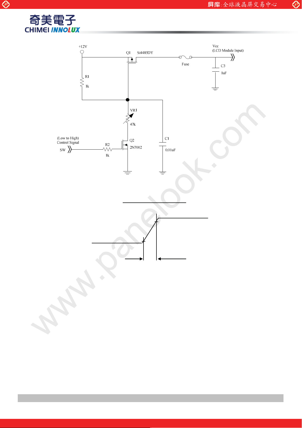
Note (3) The specified power supply current and power consumption are under the conditions at Vcc = 12 V,
Ta = 25 ± 2 ºC, f
= 120 Hz, whereas a power dissipation check pattern below is displayed.
v
Version 2.0 10 DateΚΚΚΚ03 Mar 2011
The copyright belongs to CHIMEI InnoLux. Any unauthorized use is prohibited
One step solution for LCD / PDP / OLED panel application: Datasheet, inventory and accessory!
www.panelook.com
Page 11
Global LCD Panel Exchange Center
www.panelook.com
PRODUCT SPECIFICATION
a. White Pattern
Active Area
c. Horizontal Pattern
b. Black Pattern
Active Area
Note (4) The LVDS input characteristics are as follows :
Version 2.0 11 DateΚΚΚΚ03 Mar 2011
The copyright belongs to CHIMEI InnoLux. Any unauthorized use is prohibited
One step solution for LCD / PDP / OLED panel application: Datasheet, inventory and accessory!
www.panelook.com
Page 12
Global LCD Panel Exchange Center
www.panelook.com
3.2 BACKLIGHT CONNECTOR PIN CONFIGURATION
3.2.1 LAMP SPECIFICATION (Ta = 25 ± 2 ºC)
Parameter Symbol
Min. Typ. Max.
PRODUCT SPECIFICATION
Value
Unit Note
Lamp Input Voltage VW - 840 - V
Lamp Current IL 3 14.5 15 mA
- - 1320 V
Lamp Turn On Voltage V
S
- - 1190 V
I
RMS
RMS
(1) , Ta = 0 ºC
RMS
(1) , Ta = 25 ºC
RMS
L
Operating Frequency FO 30 - 80 KHz (2)
Lamp Life Time LBL 50,000 - - Hrs (3)
3.2.2 ELECTRICAL SPECIFICATION
(Ta = 25 ± 2 ºC)
Value
Parameter Symbol
Unit Note
Min. Typ. Max.
Input High Voltage High
Input Low Voltage Low
Protection Circuit Supply
Voltage
Vcc
380 390 400 Vrms
190 195 200 V
11 13 15
V
=14.5mA
(6)
Power Consumption PIP - 145 150 W
Input Current ITB 0.372 0.385 Arms
No Dimming
(IPB input)
Measure TBB
HIGH(390V)
Oscillating Frequency FW 43 45 47 kHz
Individual Lamp Current IL 13.5 14.5 15.5 mA (5)
Connector
Detection
All Lamp Open
Detection
One Lamp
Open Detection
High CNTPRT
Vcc-0.5
Low CNTPRT
High LD
Vcc-0.5
Low LD
High OVP
Low OVP
-
-
1.25
0
- Vcc V Normal Operation
- 1 V Input Connector Open
- Vcc V Normal Operation
- 1 V All Lamp Open
- - V Normal Operation
- 0.8 V One Lamp Open
Dimming frequency FB 140 150 160 Hz
Minimum Duty Ratio D
Striking time tsriking 1
12 15 18 % Note.8
MIN
-
2 sec
Shutdown time Tsd 1 1.5 2 sec
Note (1) Lamp current is measured by utilizing AC current probe and its value is average by measuring
master and slave board.:
Version 2.0 12 DateΚΚΚΚ03 Mar 2011
The copyright belongs to CHIMEI InnoLux. Any unauthorized use is prohibited
One step solution for LCD / PDP / OLED panel application: Datasheet, inventory and accessory!
www.panelook.com
Page 13
Global LCD Panel Exchange Center
www.panelook.com
PRODUCT SPECIFICATION
Note (2) The lamp starting voltage VS should be applied to the lamp for more than 1 second after startup.
Otherwise the lamp may not be turned on.
Note (3) The lamp frequency may produce interference with horizontal synchronous frequency of the
display input signals, and it may result in line flow on the display. In order to avoid interference, the
lamp frequency should be detached from the horizontal synchronous frequency and its harmonics as
far as possible.
Note (4) The life time of a lamp is defined as when the brightness is larger than 50% of its original value and
the effective discharge length is longer than 80% of its original length (Effective discharge length is
defined as an area that has equal to or more than 70% brightness compared to the brightness at
the center point of lamp.) as the time in which it continues to operate under the condition at Ta = 25
2к and I
Note (5) Lamp current is measured master board by utilizing high frequency current meters as shown below:
Note (6) Input voltage Hv based on spec. +-7% tolerance.
Note (7) Asymmetric ratio must be from 90% to 110% (0.9<Ip/ I
Note (8) The minimum dimming under 3% operation should cause shutdown by protection circuit.
= 13.5~15.5 mArms.
L
I-p
rms@T/2XЅ2
Ip
<1.1)
T
Version 2.0 13 DateΚΚΚΚ03 Mar 2011
The copyright belongs to CHIMEI InnoLux. Any unauthorized use is prohibited
One step solution for LCD / PDP / OLED panel application: Datasheet, inventory and accessory!
www.panelook.com
Page 14

Global LCD Panel Exchange Center
www.panelook.com
PRODUCT SPECIFICATION
Balance
Board
A
A
A
A
A
A
HV (Blue +(-))
1
HV (White +(-))
2
HV (Blue +(-))
1
HV (White +(-))
2
HV (Blue +(-))
1
HV (White +(-))
2
LCD Module
A
A
A
A
A
A
HV (Blue +(-))
1
HV (White +(-))
2
HV (Blue +(-))
1
HV (White +(-))
2
HV (Blue +(-))
1
HV (White +(-))
2
Version 2.0 14 DateΚΚΚΚ03 Mar 2011
The copyright belongs to CHIMEI InnoLux. Any unauthorized use is prohibited
One step solution for LCD / PDP / OLED panel application: Datasheet, inventory and accessory!
www.panelook.com
Page 15

Global LCD Panel Exchange Center
4. BLOCK DIAGRAM OF INTERFACE
4.1 TFT LCD MODULE
CH1_0(+/-)
CH1_1(+/-)
CH1_2(+/-)
CH1_3(+/-)
CH1_4(+/-)
CH1_CLK(+/-)
CH2_0(+/-)
CH2_1(+/-)
CH2_2(+/-)
CH2_3(+/-)
CH2_4(+/-)
CH2_CLK(+/-)
CH3_0(+/-)
CH3_1(+/-)
CH3_2(+/-)
CH3_3(+/-)
CH3_4(+/-)
CH3_CLK(+/-)
CH4_0(+/-)
CH4_1(+/-)
CH4_2(+/-)
CH4_3(+/-)
CH4_4(+/-)
CH4_CLK(+/-)
(
FP7S082HA1R1200,JAE Taiwan(
INPUT CONNECTOR
ሽ
www.panelook.com
PRODUCT SPECIFICATION
TIMING CONTROLLER
DC/DC CONVERTER &
REFERENCE VOLTAGE
GENERATOR
SCAN DRIVER IC
TFT LCD PANEL
(1920x3x1080)
DATA DRIVER IC
SELLVDS
SDA
SCL
Vcc
GND
) or
IP BOARD
20037WR-H1224567(Yeon-Ho )
High
Low
Gnd
OVP
CNT_PRT
12V
LD
BALANCE
BACKLIGHT
UNIT
BOARD
Version 2.0 15 DateΚΚΚΚ03 Mar 2011
The copyright belongs to CHIMEI InnoLux. Any unauthorized use is prohibited
One step solution for LCD / PDP / OLED panel application: Datasheet, inventory and accessory!
www.panelook.com
Page 16

Global LCD Panel Exchange Center
5. INPUT TERMINAL PIN ASSIGNMENT
5.1 TFT LCD Module Input
www.panelook.com
PRODUCT SPECIFICATION
CNF1 Connector Pin Assignment (FP7S082HA1R1200,JAE Taiwan(
Pin Name Description Note
1 VCC +12V power supply
2 VCC +12V power supply
3 VCC +12V power supply
4 VCC +12V power supply
VCC +12V power supply
5
6 N.C. No Connection (1)
7 GND Ground
8 GND Ground
9 GND Ground
10 CH1[0]- First pixel Negative LVDS differential data input. Pair 0
11 CH1[0]+ First pixel Positive LVDS differential data input. Pair 0
12 CH1[1]- First pixel Negative LVDS differential data input. Pair 1
ሽ
) or equivalent)
13 CH1[1]+ First pixel Positive LVDS differential data input. Pair 1
14 CH1[2]- First pixel Negative LVDS differential data input. Pair 2
15 CH1[2]+ First pixel Positive LVDS differential data input. Pair 2
16 GND Ground
17 CH1CLK- First pixel Negative LVDS differential clock input.
18 CH1CLK+ First pixel Positive LVDS differential clock input.
19 GND Ground
20 CH1[3]- First pixel Negative LVDS differential data input. Pair 3
21 CH1[3]+ First pixel Positive LVDS differential data input. Pair 3
22 CH1[4]- First pixel Negative LVDS differential data input. Pair 4
23 CH1[4]+ First pixel Positive LVDS differential data input. Pair 4
24 GND Ground
25 CH3[0]- Third pixel Negative LVDS differential data input. Pair 0
26 CH3[0]+ Third pixel Positive LVDS differential data input. Pair 0
27 CH3[1]- Third pixel Negative LVDS differential data input. Pair 1
28 CH3[1]+ Third pixel Positive LVDS differential data input. Pair 1
Version 2.0 16 DateΚΚΚΚ03 Mar 2011
The copyright belongs to CHIMEI InnoLux. Any unauthorized use is prohibited
One step solution for LCD / PDP / OLED panel application: Datasheet, inventory and accessory!
www.panelook.com
Page 17

Global LCD Panel Exchange Center
29 CH3[2]- Third pixel Negative LVDS differential data input. Pair 2
30 CH3[2]+ Third pixel Positive LVDS differential data input. Pair 2
31 GND Ground
32 CH3CLK- Third pixel Negative LVDS differential clock input.
33 CH3CLK+ Third pixel Positive LVDS differential clock input.
34 GND Ground
35 CH3[3]- Third pixel Negative LVDS differential data input. Pair 3
36 CH3[3]+ Third pixel Positive LVDS differential data input. Pair 3
37 CH3[4]- Third pixel Negative LVDS differential data input. Pair 4
38 CH3[4]+ Third pixel Positive LVDS differential data input. Pair 4
www.panelook.com
PRODUCT SPECIFICATION
39 GND Ground
40 SCL I2C Bus
41 N.C. No Connection (1)
42 N.C. No Connection (1)
43 WP Write Protection for EEPROM
44 SDA I2C Bus
45 LVDS_SEL LVDS Data Format Selection (2)
46 N.C. No Connection (1)
47 N.C. No Connection (1)
48 N.C. No Connection (1)
49 N.C. No Connection (1)
50 N.C. No Connection (1)
51 N.C. No Connection (1)
52 GND Ground
53 CH4[4]+ Fourth pixel Positive LVDS differential data input. Pair 4
54 CH4[4]- Fourth pixel Negative LVDS differential data input. Pair 4
55 CH4[3]+ Fourth pixel Positive LVDS differential data input. Pair 3
56 CH4[3]- Fourth pixel Negative LVDS differential data input. Pair 3
57 GND Ground
58 CH4CLK+ Fourth pixel Positive LVDS differential clock input.
59 CH4CLK- Fourth pixel Negative LVDS differential clock input.
60 GND Ground
Version 2.0 17 DateΚΚΚΚ03 Mar 2011
The copyright belongs to CHIMEI InnoLux. Any unauthorized use is prohibited
One step solution for LCD / PDP / OLED panel application: Datasheet, inventory and accessory!
www.panelook.com
Page 18

Global LCD Panel Exchange Center
61 CH4[2]+ Fourth pixel Positive LVDS differential data input. Pair 2
62 CH4[2]- Fourth pixel Negative LVDS differential data input. Pair 2
63 CH4[1]+ Fourth pixel Positive LVDS differential data input. Pair 1
64 CH4[1]- Fourth pixel Negative LVDS differential data input. Pair 1
65 CH4[0]+ Fourth pixel Positive LVDS differential data input. Pair 0
66 CH4[0]- Fourth pixel Negative LVDS differential data input. Pair 0
67 GND Ground
68 CH2[4]+ Second pixel Positive LVDS differential data input. Pair 4
69 CH2[4]- Second pixel Negative LVDS differential data input. Pair 4
70 CH2[3]+ Second pixel Positive LVDS differential data input. Pair 3
www.panelook.com
PRODUCT SPECIFICATION
71 CH2[3]- Second pixel Negative LVDS differential data input. Pair 3
72 GND Ground
73 CH2CLK+ Second pixel Positive LVDS differential clock input.
74 CH2CLK- Second pixel Negative LVDS differential clock input.
75 GND Ground
76 CH2[2]+ Second pixel Positive LVDS differential data input. Pair 2
77 CH2[2]- Second pixel Negative LVDS differential data input. Pair 2
78 CH2[1]+ Second pixel Positive LVDS differential data input. Pair 1
79 CH2[1]- Second pixel Negative LVDS differential data input. Pair 1
80 CH2[0]+ Second pixel Positive LVDS differential data input. Pair 0
81 CH2[0]- Second pixel Negative LVDS differential data input. Pair 0
82 GND Ground
Note (1) Reserved for internal use. Please leave it open.
Note (2) High=connect to +3.3V: VESA Format
Note (3) Interface optional pin has internal scheme as following diagram. Customer should keep the interface
voltage level requirement as below.
Ι
Low= connect to GND or Open: JEIDA Format.
Version 2.0 18 DateΚΚΚΚ03 Mar 2011
The copyright belongs to CHIMEI InnoLux. Any unauthorized use is prohibited
One step solution for LCD / PDP / OLED panel application: Datasheet, inventory and accessory!
www.panelook.com
Page 19

Global LCD Panel Exchange Center
System Board Panel Board
www.panelook.com
PRODUCT SPECIFICATION
1K ohm
Interface Voltage Level
VH > 3.0V
VL < 0.7V
Note (4) LVDS 4-port Data Mapping
Port Channel of LVDS Data Stream
1st Port First Pixel 1, 5, 9, ……1913, 1917
2nd Port Second Pixel 2, 6, 10, ….1914, 1918
3rd Port Third Pixel 3, 7, 11, ….1915, 1919
4th Port Fourth Pixel 4, 8, 12, ….1916, 1920
IC
>20K ohm
5.2 BACKLIGHT UNIT
The pin configuration for the housing and the leader wire is shown in the table below.
Pin Name Description Wire Color
1 HV High Voltage White
2 HV High Voltage Pink
1 HV(White)
2 HV(Pink)
1 HV(White)
2 HV(Pink)
1 HV(White)
2 HV(Pink)
Version 2.0 19 DateΚΚΚΚ03 Mar 2011
The copyright belongs to CHIMEI InnoLux. Any unauthorized use is prohibited
One step solution for LCD / PDP / OLED panel application: Datasheet, inventory and accessory!
www.panelook.com
Page 20

Global LCD Panel Exchange Center
5.3 BALANCE BOARD UNIT
CN1(Header): 20037WR-H1224567(Yeon-Ho )
Pin № Signal name Feature
1 HIGH (FET) Pulse 390V (Drive, Primary)
2 No pin NC
3 LOW (FET) Blocking (195Vdc, Primary)
4 No pin
5 No pin
6 No Pin NC
www.panelook.com
PRODUCT SPECIFICATION
NC
NC
7 No Pin NC
8 GND Ground ( Secondary)
9 OVP One Lamp Open Protection
10 CNT_PRT
11 12V VCC
12 LD
Ampower: CN2-CN7: CP042EP1MFB-LF (CviLux)
Hansol: CN11-CN16: 130001WR-02H (
Pin No. Symbol Description
1
2
CCFL HOT CCFL High voltage
CCFL HOT CCFL High voltage
YEONHO
Open Input Connector Protection
(Normal 12V, Active Low)
All Lamp Open Protection
(Normal 12V, Active Low)
)
Version 2.0 20 DateΚΚΚΚ03 Mar 2011
The copyright belongs to CHIMEI InnoLux. Any unauthorized use is prohibited
One step solution for LCD / PDP / OLED panel application: Datasheet, inventory and accessory!
www.panelook.com
Page 21

Global LCD Panel Exchange Center
5.4 BLOCK DIAGRAM OF INTERFACE
www.panelook.com
PRODUCT SPECIFICATION
ARx0 +
ARx0 -
ARx1 +
ARx1 -
ARx2 +
ARx2 -
ARx3 +
ARx3 -
ARx4 +
ARx4 -
ACLK +
ACLK -
51Ω
51Ω
51Ω
51Ω
51Ω
51Ω
51Ω
51Ω
51Ω
51Ω
51Ω
51Ω
100pF
100pF
100pF
100pF
100pF
100pF
RxOUT
AR0 – AR9
AG0 – AG9
AB0 – AB9
DE
PLL
BRx0 +
BRx0 -
BRx1 +
BRx1 -
BRx2 +
BRx2 -
BRx3 +
BRx3 -
BRx4 +
BRx4 -
BCLK +
BCLK -
51Ω
51Ω
51Ω
51Ω
51Ω
51Ω
51Ω
51Ω
51Ω
51Ω
51Ω
51Ω
100pF
100pF
100pF
100pF
100pF
100pF
PLL
BR0 – BR9
BG0 – BG9
BB0 – BB9
DCLK
DCLK
Timing
Controller
LVDS Receiver
(MASTER)
LVDS INPUT
Version 2.0 21 DateΚΚΚΚ03 Mar 2011
The copyright belongs to CHIMEI InnoLux. Any unauthorized use is prohibited
One step solution for LCD / PDP / OLED panel application: Datasheet, inventory and accessory!
www.panelook.com
Page 22

Global LCD Panel Exchange Center
AR0~AR9: First pixel R data
AG0~AG9: First pixel G data
AB0~AB9: First pixel B data
BR0~BR9: Second pixel R data
BG0~BG9: Second pixel G data
BB0~BB9: Second pixel B data
DE: Data enable signal
DCLK: Data clock signal
The third and fourth pixel are followed the same rules.
CR0~CR9: Third pixel R data
CG0~CG9: Third pixel G data
www.panelook.com
PRODUCT SPECIFICATION
CB0~CB9: Third pixel B data
DR0~DR9: Fourth pixel R data
DG0~DG9: Fourth pixel G data
DB0~DB9: Fourth pixel B data
Note (1) A ~ D channel are first, second, third and fourth pixel respectively.
Note (2) The system must have the transmitter to drive the module.
Note (3) LVDS cable impedance shall be 50 ohms per signal line or about 100 ohms per twist-pair line when it is
used differentially.
Version 2.0 22 DateΚΚΚΚ03 Mar 2011
The copyright belongs to CHIMEI InnoLux. Any unauthorized use is prohibited
One step solution for LCD / PDP / OLED panel application: Datasheet, inventory and accessory!
www.panelook.com
Page 23

Global LCD Panel Exchange Center
5.5 LVDS INTERFACE
VESA Format : SELLVDS = H
JEIDA Format : SELLVDS = L or Open
VESA Format
www.panelook.com
PRODUCT SPECIFICATION
Current Cycle
AR 0P
AR 0N
AR 1P
AR 1N
AR 2P
AR 2N
AR 3P
AR 3N
AR 4P
AR 4N
JEIDA Format
AR 0P
AR 0N
AR 1P
AR 1N
AR0
AG1
AB2
AR6
AR4
AG5
AG0 AR5
AB1
DE VS HS AB5 AB4 AB3 AB2
REV AB7 AB6 AG7 AG6 AR7 AR6
REV AB9 AB8 AG9 AG8 AR9 AR8AR8 REV
AG4 AR7
AB5
AB0 AG5 AG4 AG3 AG2 AG1
AB4 AG7 AG6 AG5AG9 AG8
AR4 AR3 AR2 AR1 AR0
AR6 AR5 AR4AR9 AR8
AG0
AB1
DE
REV
AG4
AB5
AR 2P
AR 2N
AR 3P
AR 3N
AR 4P
AR 4N
AR0~AR9: First Pixel R Data (9; MSB, 0; LSB)
AG0~AG9: First Pixel G Data (9; MSB, 0; LSB)
AB0~AB9: First Pixel B Data (9; MSB, 0; LSB)
DE : Data enable signal
DCLK : Data clock signal
RSV : Reserved
AB6
AR2
DE VS HS AB7 AB6AB9 AB8
REV AB3 AB2 AG3 AG2 AR3 AR2
REV AB1 AB0 AG1 AG0 AR1 AR0AR0 REV
DE
REV
Version 2.0 23 DateΚΚΚΚ03 Mar 2011
The copyright belongs to CHIMEI InnoLux. Any unauthorized use is prohibited
One step solution for LCD / PDP / OLED panel application: Datasheet, inventory and accessory!
www.panelook.com
Page 24

Global LCD Panel Exchange Center
www.panelook.com
PRODUCT SPECIFICATION
5.6 COLOR DATA INPUT ASSIGNMENT
The brightness of each primary color (red, green and blue) is based on the 10-bit gray scale data input for the
color. The higher the binary input, the brighter the color. The table below provides the assignment of the color
versus data input.
0
0
1
0
1
0
1
1
0
0
0
:
:
0
0
0
0
0
0
:
:
1
1
1
0
0
0
:
:
0
0
0
Data Signal
0
0
0
0
1
1
0
0
1
1
0
0
1
1
1
1
0
0
0
0
0
0
:
:
:
:
0
0
0
0
0
0
0
0
0
0
0
0
:
:
:
:
1
1
1
1
1
1
0
0
0
0
0
0
:
:
:
:
0
0
0
0
0
0
0
0
0
0
0
0
0
0
0
0
0
0
0
0
0
1
1
1
0
1
0
1
1
0
0
0
:
:
0
0
0
0
0
0
:
:
1
1
1
0
0
0
:
:
0
0
0
1
0
0
0
1
1
1
0
0
0
1
1
1
1
1
1
0
0
0
0
0
0
0
0
0
:
:
:
:
:
:
0
0
0
0
0
0
0
0
0
0
0
0
0
0
0
0
0
0
:
:
:
:
:
:
1
1
1
1
1
1
1
1
1
0
0
0
0
0
0
0
0
0
:
:
:
:
:
:
0
0
0
0
0
0
0
0
0
0
1
1
0
0
0
1
1
1
1
0
0
1
1
1
0
1
1
1
0
0
0
0
0
0
0
0
0
:
:
:
:
;
:
0
0
0
0
0
0
0
0
0
0
0
0
1
0
0
0
0
1
:
:
:
:
:
:
0
1
0
1
0
0
1
1
0
0
0
0
0
0
0
0
0
0
:
:
:
:
:
:
0
0
1
0
0
1
0
0
1
0
0
0
0
0
0
0
1
1
1
1
1
1
1
1
1
0
0
0
1
1
1
0
0
0
0
0
0
0
0
0
:
:
:
:
:
:
0
0
0
0
0
0
0
0
0
0
0
0
0
0
0
0
0
0
:
:
:
:
:
:
0
0
0
0
0
0
0
0
0
0
0
0
0
0
0
0
0
0
:
:
:
:
:
:
1
1
1
1
1
1
1
1
1
Basic
Colors
Gray
Scale
Of
Red
Gray
Scale
Of
Green
Gray
Scale
Of
Blue
Color
Black
Red
Green
Blue
Cyan
Magenta
Yellow
White
Red (0) / Dark
Red (1)
Red (2)
:
:
Red (1021)
Red (1022)
Red (1023)
Green (0) / Dark
Green (1)
Green (2)
:
:
Green (1021)
Green (1022)
Green (1023)
Blue (0) / Dark
Blue (1)
Blue (2)
:
:
Blue (1021)
Blue (1022)
Blue (1023)
R9 R8 R7 R6 R5 R4 R3 R2 R1 R0 G9 G8 G7 G6 G5 G4 G3 G2 G1 G0 B9 B8 B7 B6 B5 B4 B3 B2 B1 B0
0
0
1
1
0
0
0
0
0
0
1
1
1
1
1
1
0
0
0
0
0
0
1
1
1
1
1
1
0
0
0
0
0
0
:
:
:
:
0
0
0
0
0
0
0
0
0
0
0
0
:
:
:
:
0
0
0
0
0
0
Red Green Blue
0
0
0
0
0
0
0
0
1
1
1
1
1
0
0
0
0
0
0
0
0
0
1
1
1
1
1
1
1
1
1
0
0
0
0
0
0
0
0
0
:
:
:
:
:
:
1
1
1
1
1
1
1
1
1
0
0
0
0
0
0
0
0
0
:
:
:
:
:
:
0
0
0
0
0
0
0
0
0
0
0
0
0
0
0
0
0
0
:
:
:
:
:
:
0
0
0
0
0
0
0
0
0
1
0
0
0
0
0
0
0
0
0
1
1
1
1
1
1
1
1
1
0
0
0
0
0
0
0
0
0
:
:
:
:
:
:
1
1
1
1
1
1
1
1
1
0
0
0
0
0
0
0
0
0
:
:
:
:
:
:
0
0
0
0
0
0
0
0
0
0
0
0
0
0
0
0
0
0
:
:
:
:
:
:
0
0
0
0
0
0
0
0
0
0
1
1
0
0
0
1
0
0
0
0
0
1
1
1
0
1
1
1
1
1
1
0
0
0
0
1
0
1
0
0
:
:
:
:
:
:
0
1
0
1
0
0
1
1
0
0
0
0
0
0
0
0
0
0
:
:
:
:
:
:
0
0
1
0
0
1
0
0
1
0
0
0
0
0
0
0
0
0
:
:
:
:
:
:
0
0
0
0
0
0
0
0
0
0
0
0
0
0
0
0
0
0
0
0
1
1
1
1
1
1
1
1
1
0
0
0
1
1
1
0
0
0
0
0
0
0
0
0
:
:
:
:
:
:
0
0
0
0
0
0
0
0
0
0
0
0
0
0
0
0
0
0
:
:
:
:
:
:
0
0
0
0
0
0
0
0
0
0
0
0
0
0
0
0
0
0
:
:
:
:
:
:
1
1
1
1
1
1
1
1
1
0
0
0
0
0
0
0
1
1
1
1
1
1
1
1
1
0
0
0
1
1
1
0
0
0
0
0
0
0
0
0
:
:
:
:
:
:
0
0
0
0
0
0
0
0
0
0
0
0
0
0
0
0
0
0
:
:
:
:
:
:
0
0
0
0
0
0
0
0
0
0
0
0
0
0
1
0
1
0
:
:
:
:
:
:
1
0
1
1
1
0
1
1
1
Note (1) 0: Low Level Voltage, 1: High Level Voltage
Version 2.0 24 DateΚΚΚΚ03 Mar 2011
The copyright belongs to CHIMEI InnoLux. Any unauthorized use is prohibited
One step solution for LCD / PDP / OLED panel application: Datasheet, inventory and accessory!
www.panelook.com
Page 25

Global LCD Panel Exchange Center
6. INTERFACE TIMING
6.1 INPUT SIGNAL TIMING SPECIFICATIONS
(Ta = 25 ± 2 ºC)
The input signal timing specifications are shown as the following table and timing diagram.
Signal Item Symbol Min. Typ. Max. Unit Note
LVDS
Receiver
Clock
Frequency
Input cycle to
cycle jitter
Spread spectrum
modulation range
(=1/TC)
clkin_mod
F
Spread spectrum
modulation frequency
www.panelook.com
PRODUCT SPECIFICATION
F
F
clkin
T
SSM
rcl
60 74.25 80 MHz (1)(5)
ЁЁ
F
-2%
clkin
ЁЁ
Ё
200 ps (3)
F
+2% MHz
clkin
(4)
200 KHz
LVDS
Receiver
Data
Ver t ical
Active
Display
Term
Setup Time Tlvsu 600
Hold Time Tlvhd 600
F
r5
Ё
Frame Rate
F
r6
Ё
Total Tv 1115 1125 1135 Th
Display Tvd 1080 1080 1080 Th (2)
ЁЁ
ЁЁ
100
120
Ё
Ё
ps
(5)
ps
Hz
(1)
Hz
Tv=Tvd+Tvb
Blank Tvb 35 45 55 Th (2)
Horizontal
Active
Display
Term
Total Th 540 550 575 Tc
Display Thd 480 480 480 Tc (2)
Blank Thb 60 70 95 Tc (2)
Th=Thd+Thb
Note (1) Since the module is operated in DE only mode, Hsync and Vsync input signals should be set to low
logic level. Otherwise, this module would operate abnormally.
Note (2
ʼʳ ʳ ˣ˿˸˴˸ʳ˴˾˸ʳ˸ʳ˻˸ʳ˴˺˸ʳ˹ʳ˼˸˿ʳ˶˿˶˾ʳ˻˴ʳ˹˿˿ʳ˻˸ʳ˵˸˿ʳ˸˴˼ˍʳ ʳ ʳ
˙
˶˿˾˼ʻ˴ʼ
ʳЊʳ˙
ˉ
ʳѼʳ˧ʳѼʳ˧˻
ʳ
˙
ˈ
ʳѼʳ˧ʳѼʳ˧˻ʳЊʳ˙
ʳ
ʳ
ʳ
ʳ
ʳ
ʳ
ʳ
ʳ
ʳ
˶˿˾˼ʻ˼ʼʳ
ʳ
Version 2.0 25 DateΚΚΚΚ03 Mar 2011
The copyright belongs to CHIMEI InnoLux. Any unauthorized use is prohibited
One step solution for LCD / PDP / OLED panel application: Datasheet, inventory and accessory!
www.panelook.com
Page 26

Global LCD Panel Exchange Center
DE
T
h
DCLK
T
c
DE
www.panelook.com
PRODUCT SPECIFICATION
INPUT SIGNAL TIMING DIAGRAM
T
v
T
vd
T
hd
T
hb
T
vb
DATA
Valid Display Data (480 clocks)
Note (3) The input clock cycle-to-cycle jitter is defined as below figures. Trcl = I T1 – TI
Version 2.0 26 DateΚΚΚΚ03 Mar 2011
The copyright belongs to CHIMEI InnoLux. Any unauthorized use is prohibited
One step solution for LCD / PDP / OLED panel application: Datasheet, inventory and accessory!
www.panelook.com
Page 27

Global LCD Panel Exchange Center
Note (4) The SSCG (Spread spectrum clock generator) is defined as below figures.
www.panelook.com
PRODUCT SPECIFICATION
Note (5) The LVDS timing diagram and setup/hold time is defined and showing as the following figures.
LVDS RECEIVER INTERFACE TIMING DIAGRAM
Tc
RXCLK+/-
RXn+/-
Tlvsu
Tlvhd
1T
3T
5T
7T
9T
11T
13T
14
14
14
14
14
14
14
Version 2.0 27 DateΚΚΚΚ03 Mar 2011
The copyright belongs to CHIMEI InnoLux. Any unauthorized use is prohibited
One step solution for LCD / PDP / OLED panel application: Datasheet, inventory and accessory!
www.panelook.com
Page 28

Global LCD Panel Exchange Center
6.2 POWER ON/OFF SEQUENCE
(Ta = 25 ± 2 ºC)
To prevent a latch-up or DC operation of LCD module, the power on/off sequence should be as the diagram
below.
www.panelook.com
PRODUCT SPECIFICATION
0.5ЉЉЉЉT1ЉЉЉЉ10ms
0ЉЉЉЉT
0ЉЉЉЉT
500ms ЉЉЉЉT
2
ЉЉЉЉ50ms
3
ЉЉЉЉ50ms
4
LVDS Signals
0ЉЉЉЉT7ЉЉЉЉT2
8
0ЉЉЉЉT
ЉЉЉЉT3
Option Signals
(SELLVDS)
0V
0V
0.9V
CC
0.1V
CC
Power On
T
7
0.9V
CC
0.1Vcc
T
T
1
T
2
3
T
4
VALID
Power Off
T
8
Backlight (Recommended)
500msЉЉЉЉT
100ms
ЉЉЉЉ
5
T
6
50%
T
5
50%
6
T
Power ON/OFF Sequence
Note (1) The supply voltage of the external system for the module input should follow the definition of Vcc.
Note (2) Apply the LED voltage within the LCD operation range. When the backlight turns on before the LCD
operation or the LCD turns off before the backlight turns off, the display may momentarily become
abnormal screen.
Note (3) In case of Vcc is in off level, please keep the level of input signals on the low or high impedance. If
T2<0,that maybe cause electrical overstress failure.
Note (4) T4 should be measured after the module has been fully discharged between power off and on period.
Note (5) Interface signal shall not be kept at high impedance when the power is on.
Version 2.0 28 DateΚΚΚΚ03 Mar 2011
The copyright belongs to CHIMEI InnoLux. Any unauthorized use is prohibited
One step solution for LCD / PDP / OLED panel application: Datasheet, inventory and accessory!
www.panelook.com
Page 29

Global LCD Panel Exchange Center
7. OPTICAL CHARACTERISTICS
7.1 TEST CONDITIONS
Item Symbol Value Unit
www.panelook.com
PRODUCT SPECIFICATION
Ambient Temperature Ta
Ambient Humidity Ha
Supply Voltage VCC 12 V
Input Signal According to typical value in "3. ELECTRICAL CHARACTERISTICS"
Lamp Current IL 14.5 mA
Oscillating Frequency (Balance
board)
Vertical Frame Rate Fr
The LCD module should be stabilized at given temperature for 1 hour to avoid abrupt temperature change during
measuring in a windless room.
FW
25
50
45
120
±
±
10
±
2
2
o
C
%RH
kHz
Hz
Version 2.0 29 DateΚΚΚΚ03 Mar 2011
The copyright belongs to CHIMEI InnoLux. Any unauthorized use is prohibited
One step solution for LCD / PDP / OLED panel application: Datasheet, inventory and accessory!
www.panelook.com
Page 30

Global LCD Panel Exchange Center
7.2 OPTICAL SPECIFICATIONS
The relative measurement methods of optical characteristics are shown in 7.2. The following items should be
measured under the test conditions described in 7.1 and stable environment shown in 7.1.
Item Symbol Condition Min. Typ. Max. Unit Note
Contrast Ratio CR 4000 6000 - - (2)
www.panelook.com
PRODUCT SPECIFICATION
Response Time (VA)
Center Luminance of White LC 360 500 - cd/m
White Variation
Cross Talk CT - - 4 % (5)
Red
Green
Color
Chromaticity
Blue
White
Color Gamut C.G
Gray to
gray
δ
W
Rx 0.635 -
θ
Ry 0.325 -
Gx 0.292 -
Gy 0.601 -
Bx 0.148 -
By 0.049 -
Wx 0.280 -
Wy
x=0°, θy =0
Viewing angle
at normal direction
°
- 5.5 11 ms (3)
2
(4)
- - 1.3 - (6)
Typ.
-0.03
0.290
- 72 - % NTSC
Typ.
+0.03
-
-
Viewing
Angle
Horizontal
Ver t ical
θ
θ
θ
Y+
θ
x+
x-
Y-
CR
CR
≥
20 (VA)
≥
10 (TN)
80 88 -
80 88 -
Deg. (1)
80 88 -
80 88 -
Version 2.0 30 DateΚΚΚΚ03 Mar 2011
The copyright belongs to CHIMEI InnoLux. Any unauthorized use is prohibited
One step solution for LCD / PDP / OLED panel application: Datasheet, inventory and accessory!
www.panelook.com
Page 31

Global LCD Panel Exchange Center
Note (1) Definition of Viewing Angle (θx, θy) :
Viewing angles are measured by Conoscope Cono-80 ( or Eldim EZ-Contrast 160R)
θ
x- = 90º
x-
www.panelook.com
PRODUCT SPECIFICATION
Normal
θ
x =θy = 0º
θ
y
+
θy-
θx−
θx+
12 o’clock direction
θ
y + = 90º
6 o’clock
y-
θ
y- = 90º
Note (2) Definition of Contrast Ratio (CR) :
The contrast ratio can be calculated by the following expression.
Contrast Ratio (CR) =
L255: Luminance of gray level 255
L 0: Luminance of gray level 0
CR = CR (5), where CR (X) is corresponding to the Contrast Ratio of the point X at the figure in Note
(6).
Note (3) Definition of Gray-to-Gray Switching Time:
100%
90%
x
+
θ
x+ = 90º
L255of LuminanceSurface
L0 of LuminanceSurface
Optical
Response
10%
0%
Gray to gray
switching time
Gray to gray
switching time
Time
The driving signal means the signal of gray level 0, 31, 63, 95, 127, 159, 191, 223 and 255
Gray to gray means the average switching time of gray level 0, 31, 63, 95, 127, 159, 191, 223 and
255 to each other.
#!
Version 2.0 31 DateΚΚΚΚ03 Mar 2011
The copyright belongs to CHIMEI InnoLux. Any unauthorized use is prohibited
One step solution for LCD / PDP / OLED panel application: Datasheet, inventory and accessory!
www.panelook.com
Page 32

Global LCD Panel Exchange Center
!!!!
Note (3) Definition of Response Time (TR, TF):
www.panelook.com
PRODUCT SPECIFICATION
Gray Level 255
100%
90%
Optical
Response
10%
0%
Note (4) Definition of Luminance of White (L
Measure the luminance of gray level 255 at center point and 5 points
L
= L (5), where L (X) is corresponding to the luminance of the point X at the figure in Note (6).
C
Gray Level 255
Gray Level 0
T
R
):
C
T
F
Time
Version 2.0 32 DateΚΚΚΚ03 Mar 2011
The copyright belongs to CHIMEI InnoLux. Any unauthorized use is prohibited
One step solution for LCD / PDP / OLED panel application: Datasheet, inventory and accessory!
www.panelook.com
Page 33

Global LCD Panel Exchange Center
A
(
)
A
(
)
(
)
A
(
)
A
(
)
Note (5) Definition of Cross Talk (CT):
www.panelook.com
PRODUCT SPECIFICATION
CT = | Y
– YA | / Y
B
×
100 (%)
A
Where:
Y
= Luminance of measured location without gray level 0 pattern (cd/m2)
A
Y
= Luminance of measured location with gray level 0 pattern (cd/m2)
B
ctive Area
(0, 0)
Y
(D/2,W/8)
A, U
0, 0
(D/4,W/4)
Gray 128
Y
(D/8,W/2)
A, L
(D/2,7W/8)
Y
A, D
= Luminance of measured location without gray level 255 pattern (cd/m2)
Y
A
Y
= Luminance of measured location with gray level 255 pattern (cd/m2)
B
(7D/8,W/2)
Y
A, R
D, W
Y
(D/8,W/2)
B, L
ctive Area
Y
Y
(D/2,W/8)
B, U
Y
(3D/4,3W/4)
(D/2,7W/8)
B, D
(7D/8,W/2)
B, R
(0, 0)
(D/8,W/2)
Y
A, L
ctive Area
Y
Gray 128
Y
(D/2,W/8)
A, U
(D/2,7W/8)
A, D
(7D/8,W/2)
Y
A, R
D, W
0, 0
Y
(D/8,W/2)
B, L
(D/4,W/4)
ctive Area
Y
Gray 255
Y
(D/2,W/8)
B, U
Y
(3D/4,3W/4)
(D/2,7W/8)
B, D
(7D/8,W/2)
B, R
D, W
Version 2.0 33 DateΚΚΚΚ03 Mar 2011
The copyright belongs to CHIMEI InnoLux. Any unauthorized use is prohibited
One step solution for LCD / PDP / OLED panel application: Datasheet, inventory and accessory!
www.panelook.com
Page 34

Global LCD Panel Exchange Center
Note (6) Definition of White Variation (δW):
Measure the luminance of gray level 255 at 5 points
δ
W = Maximum [L (1), L (2), L (3), L (4), L (5)] / Minimum [L (1), L (2), L (3), L (4), L (5)]
www.panelook.com
PRODUCT SPECIFICATION
Horizontal Line
D
D/4 D/2 3D/4
Vertical Line
W
W/4
W/2
1 2
5
3 4
Active Area
: Test Point
X=1 to 5
Version 2.0 34 DateΚΚΚΚ03 Mar 2011
The copyright belongs to CHIMEI InnoLux. Any unauthorized use is prohibited
One step solution for LCD / PDP / OLED panel application: Datasheet, inventory and accessory!
www.panelook.com
Page 35

Global LCD Panel Exchange Center
www.panelook.com
PRODUCT SPECIFICATION
PRECAUTIONS
8.1 ASSEMBLY AND HANDLING PRECAUTIONS
[ 1 ] Do not apply rough force such as bending or twisting to the module during assembly.
[ 2 ] It is recommended to assemble or to install a module into the user’s system in clean working areas. The
dust and oil may cause electrical short or worsen the polarizer.
[ 3 ] Do not apply pressure or impulse to the module to prevent the damage of LCD panel and Backlight.
[ 4 ] Always follow the correct power-on sequence when the LCD module is turned on. This can prevent the
damage and latch-up of the CMIS LSI chips.
[ 5 ] Bezel of Set can not press or touch the panel surface. It will make light leakage or scrape.
[ 6 ] Do not plug in or pull out the I/F connector while the module is in operation.
[ 7 ] Do not disassemble the module.
[ 8 ] Use a soft dry cloth without chemicals for cleaning, because the surface of polarizer is very soft and easily
scratched.
[ 9 ] Moisture can easily penetrate into LCD module and may cause the damage during operation.
[ 10 ] When storing modules as spares for a long time, the following precaution is necessary.
[ 10.1 ] Do not leave the module in high temperature, and high humidity for a long time. It is highly
recommended to store the module with temperature from 0 to 35
condensation.
[ 10.2 ] The module shall be stored in dark place. Do not store the TFT-LCD module in direct sunlight or
fluorescent light.
[ 11 ] When ambient temperature is lower than 10ºC, the display quality might be reduced. For example, the
response time will become slow, and the starting voltage of CCFL will be higher than that of room
temperature.
к
at normal humidity without
8.2 SAFETY PRECAUTIONS
[ 1 ] The startup voltage of a Backlight is approximately 1000 Volts. It may cause an electrical shock while
assembling with the inverter. Do not disassemble the module or insert anything into the Backlight unit.
[ 2 ] If the liquid crystal material leaks from the panel, it should be kept away from the eyes or mouth. In case of
contact with hands, skin or clothes, it has to be washed away thoroughly with soap.
[ 3 ] After the module’s end of life, it is not harmful in case of normal operation and storage.
Version 2.0 35 DateΚΚΚΚ03 Mar 2011
The copyright belongs to CHIMEI InnoLux. Any unauthorized use is prohibited
One step solution for LCD / PDP / OLED panel application: Datasheet, inventory and accessory!
www.panelook.com
Page 36

Global LCD Panel Exchange Center
9. DEFINITION OF LABELS
9.1 CMI MODULE LABEL
The barcode nameplate is pasted on each module as illustration, and its definitions are as following explanation.
www.panelook.com
PRODUCT SPECIFICATION
V400H1 –LHA Rev. XX
CHI MEI
OPTOELECTRONICS
(a) Model Name: V400H1-LHA
(b) Revision: Rev. XX, for example: A0, A1… B1, B2… or C1, C2…etc.
(c) Production Locations / Factory ID: IN TAIWAN (GEMN) or IN CHINA (LEOO or CAPG or CANO)
(d) CMI barcode definition:
Serial ID: XX-XX-X-XX-YMD-L-NNNN
Code Meaning Description
XX CMI internal use XX Revision Cover all the change
X-XX CMI internal use -
Year, month, day
YMD
L Product line # Line 1=1, Line 2=2, Line 3=3, …
NNNN Serial number Manufacturing sequence of product
(e) Customer’s barcode definition:
X X X X X X X Y M D L N N N N
CM40H12XXXXXLXXLYMDNNNN
Year: 2001=1, 2002=2, 2003=3, 2004=4…
Month: Jan. ~ Dec.=1, 2, 3, ~, 9, A, B, C
st
Day: 1
to 31st =1, 2, 3, ~, 9, A, B, C, ~, W, X, Y, exclude I, O, and U
E207943
MADE IN TAIWAN
RoHS GEMN
Serial ID: CM-40HHA-X-X-X-XX-L-XX-L-YMD-NNNN
Code Meaning Description
CM Supplier code CMI=CM
40HHA
XX
XX
YMD
NNNN Serial number
Model number
X Revision code C1=1, C2=2, ……C9=9
Source driver IC code
X
Gate driver IC code
X
Cell location Tainan, Taiwan=TN
L Cell line # 1~12=0~C
Module location Tainan, Taiwan=TN
Module line # 1~12=0~C
L
Year, month, day
V400H1-LHA=40HHA
Century=1, CLL=2, Demos=3, Epson=4, Fujitsu=5, Himax=6,
Hitachi=7, Hynix=8, LDI=9, Matsushita=A, NEC=B, Novatec=C,
OKI=D, Philips=E, Renasas=F, Samsung=G, Sanyo=H, Sharp=I,
TI=J, Topro=K, Toshiba=L, Windbond=M
Year: 2001=1, 2002=2, 2003=3, 2004=4…
Month: Jan. ~ Dec.=1, 2, 3, ~, 9, A, B, C
st
Day: 1
By LCD supplier
to 31st =1, 2, 3, ~, 9, A, B, C, ~, W, X, Y, exclude I, O, and U
Version 2.0 36 DateΚΚΚΚ03 Mar 2011
The copyright belongs to CHIMEI InnoLux. Any unauthorized use is prohibited
One step solution for LCD / PDP / OLED panel application: Datasheet, inventory and accessory!
www.panelook.com
Page 37

Global LCD Panel Exchange Center
10. PACKAGING
10.1 PACKAGING SPECIFICATIONS
(1) 5 LCD TV modules / 1 Box
(2) Box dimensions : 1060(L)x378(W)x650(H)mm
(3) Weight : Approx. 44Kg(5 modules per carton)
(4) 5 LCD TV modules / 1 Box
(5) Box dimensions : 1060(L)x378(W)x650(H)mm
(6) Weight :
a. Panel module each pcs: 7.8 kg
b. Panel Packing Box
- Cushion: 1.55 kg (5pcs per box)
- Carton: 2.73 kg
www.panelook.com
PRODUCT SPECIFICATION
- Panel: 7.8 kg x 5pcs = 39 kg
-Panel Packing Box Total (1 Box) =43.28 kg
c. Total Packing weight
1) For Vessel shipment Pallet (1 Pallet =3 Box or 6 Box)
- Pallet weight: 13.48 kg
- Pallet Cushion: 4.65 kg or 9.3 kg
- Pallet Packing Total = 143.32 kg or 273.16 kg
2) For Air shipment Pallet (1 Pallet =6 Box)
- Pallet weight: 13.48 kg
- Pallet Cushion: 9.3 kg
- Pallet Packing Total =273.16 kg
Version 2.0 37 DateΚΚΚΚ03 Mar 2011
The copyright belongs to CHIMEI InnoLux. Any unauthorized use is prohibited
One step solution for LCD / PDP / OLED panel application: Datasheet, inventory and accessory!
www.panelook.com
Page 38

Global LCD Panel Exchange Center
10.2 PACKAGING METHOD
Figures 10-1 and 10-2 are the packing method
www.panelook.com
PRODUCT SPECIFICATION
Figure 10-1 packing method
Version 2.0 38 DateΚΚΚΚ03 Mar 2011
The copyright belongs to CHIMEI InnoLux. Any unauthorized use is prohibited
One step solution for LCD / PDP / OLED panel application: Datasheet, inventory and accessory!
www.panelook.com
Page 39

Global LCD Panel Exchange Center
www.panelook.com
PRODUCT SPECIFICATION
Figure 10-2 packing method
Version 2.0 39 DateΚΚΚΚ03 Mar 2011
The copyright belongs to CHIMEI InnoLux. Any unauthorized use is prohibited
One step solution for LCD / PDP / OLED panel application: Datasheet, inventory and accessory!
www.panelook.com
Page 40

Global LCD Panel Exchange Center
11. MECHANICAL CHARACTERISTIC
www.panelook.com
PRODUCT SPECIFICATION
Version 2.0 40 DateΚΚΚΚ03 Mar 2011
The copyright belongs to CHIMEI InnoLux. Any unauthorized use is prohibited
One step solution for LCD / PDP / OLED panel application: Datasheet, inventory and accessory!
www.panelook.com
Page 41

Global LCD Panel Exchange Center
www.panelook.com
PRODUCT SPECIFICATION
Version 2.0 41 DateΚΚΚΚ03 Mar 2011
The copyright belongs to CHIMEI InnoLux. Any unauthorized use is prohibited
One step solution for LCD / PDP / OLED panel application: Datasheet, inventory and accessory!
www.panelook.com
Page 42

Global LCD Panel Exchange Center
www.panelook.com
PRODUCT SPECIFICATION
Version 2.0 42 DateΚΚΚΚ03 Mar 2011
The copyright belongs to CHIMEI InnoLux. Any unauthorized use is prohibited
One step solution for LCD / PDP / OLED panel application: Datasheet, inventory and accessory!
www.panelook.com
Page 43

Global LCD Panel Exchange Center
www.panelook.com
Appendix – TWO Wire BUS INTRODUCTION
A.1 PIN ASSIGNMENT
51pins LVDS connector
Pin8: SCL
Pin9: SDA
A.2 I2C BUS APPLICATION NOTE
I2C bus: (The I2C bus must for MEMC only or prevent the I2C bus voltage drop down in initial state)
PRODUCT SPECIFICATION
A.3 TWO WIRE BUS DEVICE ADDRESS
Two wire device address: default is 0x40, 1 byte
Two wire command: the range is 0x00 to 0xFF, 1 byte, see the two wire command table.
Version 2.0 43 DateΚΚΚΚ03 Mar 2011
The copyright belongs to CHIMEI InnoLux. Any unauthorized use is prohibited
One step solution for LCD / PDP / OLED panel application: Datasheet, inventory and accessory!
www.panelook.com
 Loading...