

Page 1
Global LCD Panel Exchange Center
TFT LCD Preliminary Specification
MODEL NO.: V400H1 - L04
ʳ
ʳ
www.panelook.com
Issued Date: Oct. 29, 2008
Model No.: V400H1 - L04
Preliminary
ʳ
TVHD
Approved By
LY Chen
QA Dept. Product Development Div.
Reviewed By
Kc-Ko WT Lin
LCD TV Marketing and Product Management Div.
Prepared By
WY Li Alan Chang
1
The information described in this technical specification is tentative and it is possible to be changed without prior notice.
Please contact CMO ’s representative while your product design is based on this specification.
One step solution for LCD / PDP / OLED panel application: Datasheet, inventory and accessory!
Version 1.0
www.panelook.com
Page 2
Global LCD Panel Exchange Center
www.panelook.com
Issued Date: Oct. 29, 2008
Model No.: V400H1 - L04
Preliminary
- CONTENTS -
REVISION HISTORY
1. GENERAL DESCRIPTION
1.1 OVERVIEW
1.2 FEATURES
1.3 APPLICATION
1.4 GENERAL SPECIFICATIONS
1.5 MECHANICAL SPECIFICATIONS
2. ABSOLUTE MAXIMUM RATINGS
2.1 ABSOLUTE RATINGS OF ENVIRONMENT
2.2 PACKAGE STORAGE
2.3 ELECTRICAL ABSOLUTE RATINGS
2.3.1 TFT LCD MODULE
2.3.2 BACKLIGHT UNIT
3. ELECTRICAL CHARACTERISTICS
3.1 TFT LCD MODULE
3.2 BACKLIGHT UNIT
3.2.1 CCFL(Cold Cathode Fluorescent Lamp) CHARACTERISTICS
3.2.2 BALANCE BOARD CHARACTERISTICS
4. BLOCK DIAGRAM
4.1 TFT LCD MODULE
-------------------------------------------------------
-------------------------------------------------------
-------------------------------------------------------
-------------------------------------------------------
-------------------------------------------------------
3
4
5
7
11
5. INTERFACE PIN CONNECTION
5.1 TFT LCD MODULE
5.2 BACKLIGHT UNIT
5.3 BALANCE BOARD UNIT
5.4 BLOCK DIAGRAM OF INTERFACE
5.5 LVDS INTERFACE
5.6 COLOR DATA INPUT ASSIGNMENT
6. INTERFACE TIMING
6.1 INPUT SIGNAL TIMING SPECIFICATIONS
6.2 POWER ON/OFF SEQUENCE
7. OPTICAL CHARACTERISTICS
7.1 TEST CONDITIONS
7.2 OPTICAL SPECIFICATIONS
8. DEFINITION OF LABELS
8.1 CMO MODULE LABEL
9. PACKAGING
9.1 PACKING SPECIFICATIONS
9.2 PACKING METHOD
10. PRECAUTIONS
10.1 ASSEMBLY AND HANDLING PRECAUTIONS
10.2 SAFETY PRECAUTIONS
10.3 SAFETY STANDARDS
-------------------------------------------------------
-------------------------------------------------------
-------------------------------------------------------
-------------------------------------------------------
-------------------------------------------------------
-------------------------------------------------------
12
21
24
28
29
31
11. MECHANICAL CHARACTERISTICS
The information described in this technical specification is tentative and it is possible to be changed without prior notice.
Please contact CMO ’s representative while your product design is based on this specification.
One step solution for LCD / PDP / OLED panel application: Datasheet, inventory and accessory!
-------------------------------------------------------
2
Version 1.0
www.panelook.com
32
Page 3
Global LCD Panel Exchange Center
www.panelook.com
Issued Date: Oct. 29, 2008
Model No.: V400H1 - L04
Preliminary
REVISION HISTORY
Version Date
Ver 1.0 Oct. 29,’08 All All Preliminary Specification was first issued.
Page
(New)
Section Description
3
The information described in this technical specification is tentative and it is possible to be changed without prior notice.
Please contact CMO ’s representative while your product design is based on this specification.
One step solution for LCD / PDP / OLED panel application: Datasheet, inventory and accessory!
Version 1.0
www.panelook.com
Page 4
Global LCD Panel Exchange Center
1. GENERAL DESCRIPTION
1.1 OVERVIEW
V400H1- L04 is a 40” TFT Liquid Crystal Display module with 16-CCFL Backlight unit and 2ch-LVDS
interface. This module supports 1920 x 1080 FHD format and can display true 16.7M colors (8-bit colors).
The inverter module for backlight is built-in.
1.2 FEATURES
- High brightness (500 nits)
- Ultra-high contrast ratio (4000:1)
- Faster response time (Gray to gray average 6.5ms)
- High color saturation NTSC 72%
- Ultra wide viewing angle : 176(H)/176(V) (CR>20) with Super MVA technology
www.panelook.com
Issued Date: Oct. 29, 2008
Model No.: V400H1 - L04
Preliminary
- DE (Data Enable) only mode
- LVDS (Low Voltage Differential Signaling) interface
- Color reproduction (nature color)
- Optimized response time for both 50/60 Hz Frame rate
- Low color shift function
- RoHS compliance
1.3 APPLICATION
- TFT LCD TVs
- Multi-Media Display
1.4 GENERAL SPECIFICATI0NS
Item Specification Unit Note
Active Area 885.6(H) x 498.15 (V) (40” diagonal) mm
Bezel Opening Area 891.7 (H) x 504.2 (V) mm
Driver Element a-si TFT active matrix -
Pixel Number 1920 x R.G.B. x 1080 pixel
Pixel Pitch (Sub Pixel) 0.15375 (H) x 0.46125 (V) mm
Pixel Arrangement RGB vertical stripe -
Display Colors 16.7M color
Display Operation Mode Transmissive mode / Normally black -
Surface Treatment Anti-Glare coating (Haze 17%), Hard coating (3H) -
(1)
1.5 MECHANICAL SPECIFICATIONS
Item Min. Typ. Max. Unit Note
Horizontal(H) 951 952 953 mm (1)
Vertical(V) 550 551 552 mm (1)
Module Size
Note (1) Please refer to the attached drawings for more information of front and back outline dimensions.
The information described in this technical specification is tentative and it is possible to be changed without prior notice.
Please contact CMO ’s representative while your product design is based on this specification.
One step solution for LCD / PDP / OLED panel application: Datasheet, inventory and accessory!
Depth(D) 45.6 46.6 47.6 mm To PCB cover
Depth(D) 52.2 53.2 54.2 mm
Weight - 9460 - g
4
To Balance Board
cover
Version 1.0
www.panelook.com
Page 5
Global LCD Panel Exchange Center
2. ABSOLUTE MAXIMUM RATINGS
2.1 ABSOLUTE RATINGS OF ENVIRONMENT
Item Symbol
Storage Temperature TST -20 +60 ºC (1)
Operating Ambient Temperature T
Shock (Non-Operating) S
Vibration (Non-Operating) V
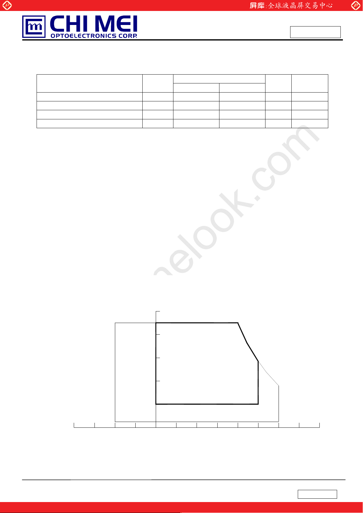
Note (1) Temperature and relative humidity range is shown in the figure below.
(a) 90 %RH Max. (Ta Љ 40 ºC).
(b) Wet-bulb temperature should be 39 ºC Max. (Ta > 40 ºC).
(c) No condensation.
Note (2) The maximum operating temperature is based on the test condition that the surface temperature of
www.panelook.com
Issued Date: Oct. 29, 2008
Model No.: V400H1 - L04
Preliminary
Value
Min. Max.
OP
- 50 G (3), (5)
NOP
- 1.0 G (4), (5)
NOP
0 +50 ºC (1), (2)
Unit Note
display area is less than or equal to 65 ºC with LCD module alone in a temperature controlled chamber.
Thermal management should be considered in final product design to prevent the surface temperature of
display area from being over 65 ºC. The range of operating temperature may degrade in case of improper
thermal management in final product design.
Note (3) 11 ms, half sine wave, 1 time for ± X, ± Y, ± Z.
Note (4) 10 ~ 200 Hz, 10 min, 1 time each X, Y, Z.
Note (5) At testing Vibration and Shock, the fixture in holding the module has to be hard and rigid enough
so that the module would not be twisted or bent by the fixture.
Relative Humidity (%RH)
100
90
80
60
Operating Range
40
20
10
Storage Range
Temperature (ºC)
5
The information described in this technical specification is tentative and it is possible to be changed without prior notice.
Please contact CMO ’s representative while your product design is based on this specification.
One step solution for LCD / PDP / OLED panel application: Datasheet, inventory and accessory!
Version 1.0
www.panelook.com
8060-20 400 20-40
Page 6
Global LCD Panel Exchange Center
2.2 PACKAGE STORAGE
When storing modules as spares for a long time, the following precaution is necessary.
(a) Do not leave the module in high temperature, and high humidity for a long time. It is highly recommended to
store the module with temperature from 0 to 35 ºC at normal humidity without condensation.
(b) The module shall be stored in dark place. Do not store the TFT-LCD module in direct sunlight or fluorescent
light.
2.3 ELECTRICAL ABSOLUTE RATINGS
2.3.1 TFT LCD MODULE
Item Symbol
Power Supply Voltage Vcc -0.3 13.5 V
Input Signal Voltage VIN -0.3 3.6 V
www.panelook.com
Value
Min. Max.
Issued Date: Oct. 29, 2008
Model No.: V400H1 - L04
Preliminary
Unit Note
(1)
2.3.2 BACKLIGHT UNIT
Item Symbol
Lamp Voltage V
Note (1) No moisture condensation or freezing.
W
Value
Min. Max.
Ё
3000 V
Unit Note
RMS
6
The information described in this technical specification is tentative and it is possible to be changed without prior notice.
Please contact CMO ’s representative while your product design is based on this specification.
One step solution for LCD / PDP / OLED panel application: Datasheet, inventory and accessory!
Version 1.0
www.panelook.com
Page 7
Global LCD Panel Exchange Center
3. ELECTRICAL CHARACTERISTICS
www.panelook.com
Issued Date: Oct. 29, 2008
Model No.: V400H1 - L04
Preliminary
3.1 TFT LCD MODULE
Parameter Symbol
Ta = 25 ± 2 ºC
Value
Min. Typ. Max.
Unit Note
Power Supply Voltage VCC 10.8 12.0 13.2 V (1)
Power Supply Ripple Voltage VRP - - 350 mV
Rush Current I
- - 4.5 A (2)
RUSH
White - 1.2 1.5 A
Power Supply Current
LVDS
Interface
CMOS
interface
Common Input Voltage V
Terminating Resistor R
Input High Threshold Voltage VIH 2.7 - 3.3 V
Input Low Threshold Voltage V
Black - 0.6 0.7 A
Vertical Stripe
I
CC
(3)
- 1.0 1.2 A
1.125 1.25 1.375 V
LVC
- 100 - ohm
T
0 - 0.7 V
IL
Note (1) The module should be always operated within above ranges.
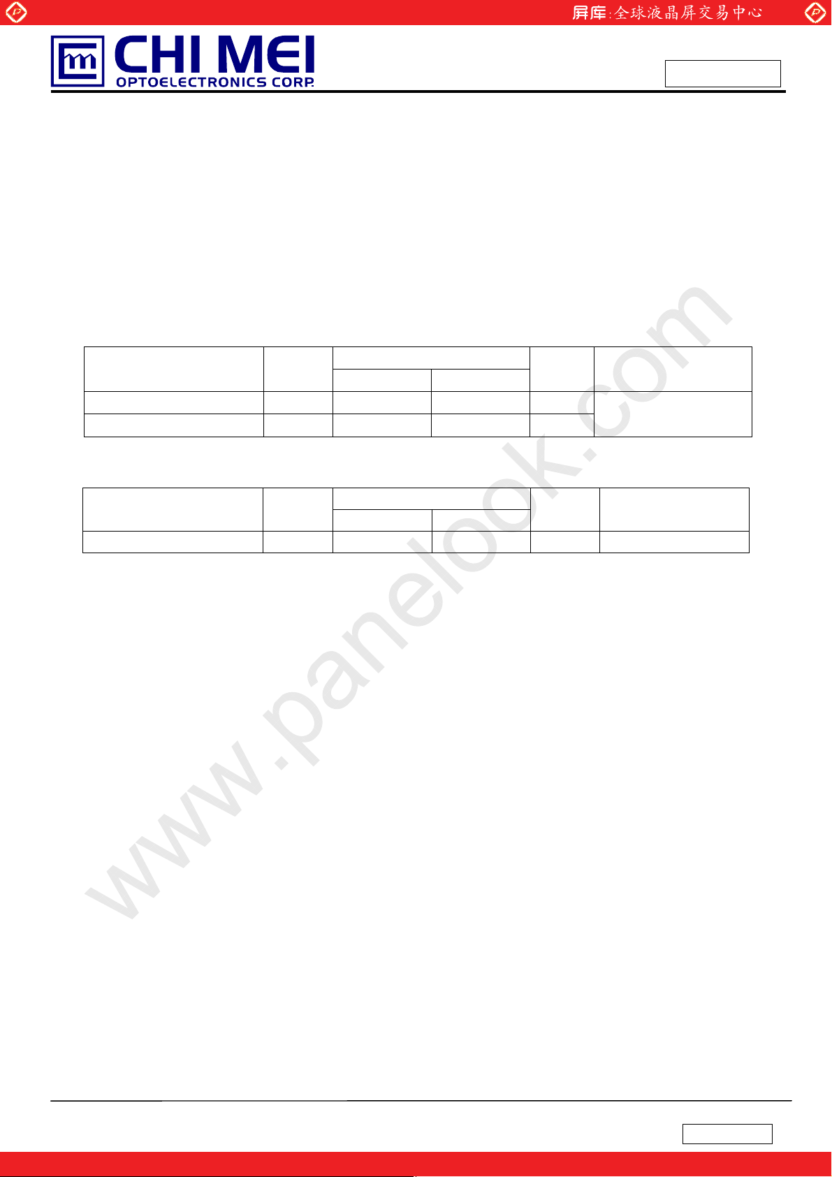
Note (2) Measurement Conditions:
+12v
Vcc rising time is 470us
+12V
0.9Vcc
0.1Vcc
GND
470us
7
The information described in this technical specification is tentative and it is possible to be changed without prior notice.
Please contact CMO ’s representative while your product design is based on this specification.
One step solution for LCD / PDP / OLED panel application: Datasheet, inventory and accessory!
Version 1.0
www.panelook.com
Page 8
Global LCD Panel Exchange Center
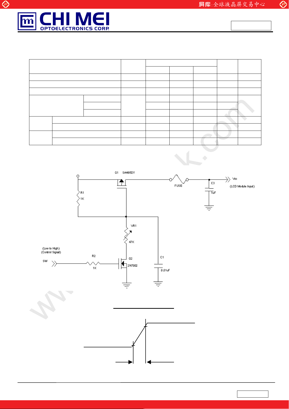
Note (3) The specified power supply current is under the conditions at Vcc = 12 V, Ta = 25 ± 2 ºC, fv = 60
Hz, whereas a power dissipation check pattern below is displayed.
www.panelook.com
Issued Date: Oct. 29, 2008
Model No.: V400H1 - L04
Preliminary
a. White Pattern
Active Area
c. Vertical Stripe Pattern
b. Black Pattern
Active Area
R
G
R
B
G
B
B
R
R
G
G
B
B
R
R
B
R R
Active Area
3.2 BACKLIGHT UNIT
3.2.1 CCFL (Cold Cathode Fluorescent Lamp) CHARACTERISTICS (
Parameter Symbol
Lamp Voltage V
Lamp Current I
Lamp Starting Voltage V
Operating Frequency FO 30 - 80
Lamp Life Time LBL 50,000 - -
W
L
S
Min. Typ. Max.
- 1100 -
9.7 10 10.3
- -
- -
Value
2000
1600
R
G
G
B
G
B
Ta = 25 ± 2 ºC)
V
mA
V
V
B
R
G
B
Unit Note
Ih = 10.0mA
RMS
RMS
RMS
RMS
KHz (3)
Hrs 10.5mA
(1)
(2), Ta = 0 ºC
(2), Ta = 25 ºC
8
The information described in this technical specification is tentative and it is possible to be changed without prior notice.
Please contact CMO ’s representative while your product design is based on this specification.
One step solution for LCD / PDP / OLED panel application: Datasheet, inventory and accessory!
Version 1.0
www.panelook.com
Page 9
Global LCD Panel Exchange Center
)
(LD)
www.panelook.com
Issued Date: Oct. 29, 2008
Model No.: V400H1 - L04
Preliminary
3.2.2 BALANCE BOARD CHARACTERISTICS (
Parameter Symbol
Ta = 25 ± 2 ºC)
Value
Unit Note
Min. Typ. Max.
Input High Voltage V
Protection Circuit Supply Voltage Vcc
Input Current I
Oscillating Frequency
Individual Lamp Current I
Lamp Detection
High (LD
Low
(HV1/HV2)
BL(HV)
F
LD
LD
52.5 55.5 58.5 kHz
W
10.7 11.0 11.3 mA H.V
L
- 1250 - V (2)
10 12 14 V
- 175 - mArms No Dimming
9.5
-
--
- 1.0
V Normal Operation
V Lamp Connector Open
Dimming frequency FB 120 150 180 Hz
Minimum Duty Ratio D
- 20 - %
MIN
Note (1) Lamp current is measured by utilizing high frequency current meters as shown below:
Note (2) Input High Voltage Hv based on spec. +-7% tolerance.
Note (3) Asymmetric ratio must be from 90% to 110% (0.9<Ip/ I
rms@T/2XЅ2
<1.1)
I-p
T
Ip
9
The information described in this technical specification is tentative and it is possible to be changed without prior notice.
Please contact CMO ’s representative while your product design is based on this specification.
One step solution for LCD / PDP / OLED panel application: Datasheet, inventory and accessory!
Version 1.0
www.panelook.com
Page 10
Global LCD Panel Exchange Center
A
A
A
A
A
A
A
A
www.panelook.com
HV (Blue +)
1
HV (White -)
2
HV (Blue +)
1
HV (White -)
2
HV (Blue +)
1
HV (White -)
2
HV (Blue +)
1
HV (White -)
2
Issued Date: Oct. 29, 2008
Model No.: V400H1 - L04
Preliminary
Balance
Board
A
A
A
A
A
A
A
A
HV (Blue +)
1
HV (White -)
2
HV (Blue +)
1
HV (White -)
2
HV (Blue +)
1
HV (White -)
2
HV (Blue +)
1
HV(White -)
2
LCD Module
10
The information described in this technical specification is tentative and it is possible to be changed without prior notice.
Please contact CMO ’s representative while your product design is based on this specification.
One step solution for LCD / PDP / OLED panel application: Datasheet, inventory and accessory!
Version 1.0
www.panelook.com
Page 11

Global LCD Panel Exchange Center
4. BLOCK DIAGRAM
4.1 TFT LCD MODULE
ORX0(+/-)
ORX1(+/-)
ORX2(+/-)
ORX3(+/-)
OCLK(+/-)
SCL
SDA
WP
SELLVDS
ODSEL
ERX0(+/-)
ERX1(+/-)
ERX2(+/-)
ERX3(+/-)
ECLK(+/-)
Vcc
GND
INPUT CONNECTOR
(FI-RE51S-HF )
CNF1
www.panelook.com
FRAME BUFFER
TIMING
CONTROLLER
DC/DC CONVERTER &
REFERENCE VOLTAGE
Issued Date: Oct. 29, 2008
Model No.: V400H1 - L04
Preliminary
SCAN DRIVER IC
TFT LCD PANEL
(1920x3x1080)
DATA DRIVER IC
CN125: KN30-7P-1.25H (Hirose)
IP Board
+
-
CN101: MDF61-4P-13V(21)(HIROSE)
BALANCE
BOARD
BACKLIGHT
UNIT
CN201 - CN208 : CP042EP1MFB-LF
11
The information described in this technical specification is tentative and it is possible to be changed without prior notice.
Please contact CMO ’s representative while your product design is based on this specification.
One step solution for LCD / PDP / OLED panel application: Datasheet, inventory and accessory!
Version 1.0
www.panelook.com
Page 12

Global LCD Panel Exchange Center
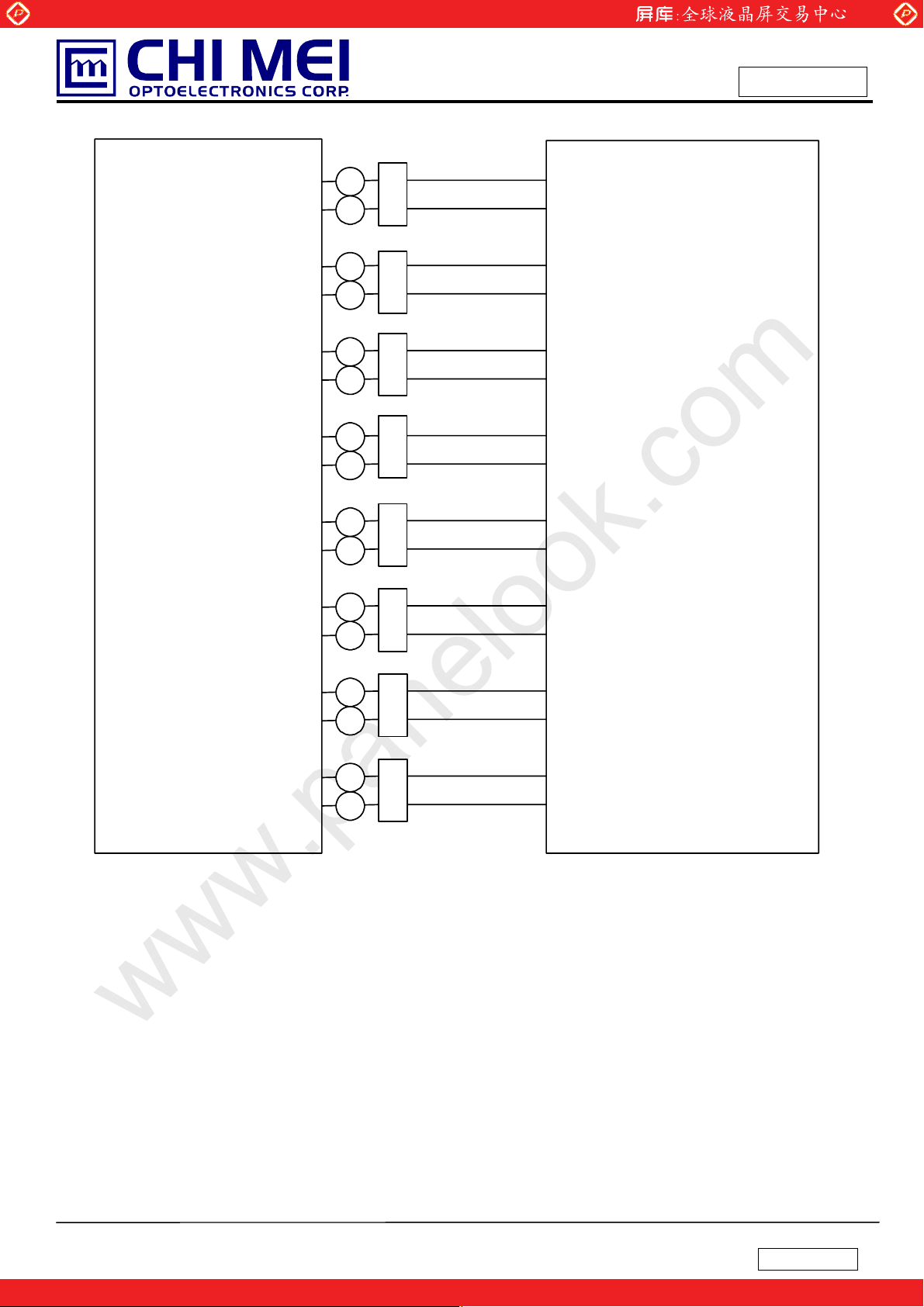
5. INTERFACE PIN CONNECTION
5.1 TFT LCD MODULE
CNF1 Connector Pin Assignment
Pin Name Description Note
1 VCC +12V power supply
2 VCC +12V power supply
3 VCC +12V power supply
4 VCC +12V power supply
5 VCC +12V power supply
6 GND Ground
7 GND Ground
8 GND Ground
www.panelook.com
Issued Date: Oct. 29, 2008
Model No.: V400H1 - L04
Preliminary
9 GND Ground
10 ORX0- Odd pixel, Negative LVDS differential data input. Channel 0
11 ORX0+ Odd pixel, Positive LVDS differential data input. Channel 0
12 ORX1- Odd pixel, Negative LVDS differential data input. Channel 1
13 ORX1+ Odd pixel, Positive LVDS differential data input. Channel 1
14 ORX2- Odd pixel, Negative LVDS differential data input. Channel 2
15 ORX2+ Odd pixel, Positive LVDS differential data input. Channel 2
16 GND Ground
17 OCLK- Odd pixel, Negative LVDS differential clock input
18 OCLK+ Odd pixel, Positive LVDS differential clock input.
19 GND Ground
20 ORX3- Odd pixel, Negative LVDS differential data input. Channel 3
21 ORX3+ Odd pixel, Positive LVDS differential data input. Channel 3
22 N.C. No Connection
23 N.C. No Connection
24 GND Ground
(1)
25 ERX0- Even pixel Negative LVDS differential data input. Channel 0
26 ERX0+ Even pixel Positive LVDS differential data input. Channel 0
27 ERX1- Even pixel Negative LVDS differential data input. Channel 1
28 ERX1+ Even pixel Positive LVDS differential data input. Channel 1
29 ERX2- Even pixel Negative LVDS differential data input. Channel 2
30 ERX2+ Even pixel Positive LVDS differential data input. Channel 2
31 GND Ground
32 ECLK- Even pixel Negative LVDS differential clock input.
33 ECLK+ Even pixel Positive LVDS differential clock input.
12
The information described in this technical specification is tentative and it is possible to be changed without prior notice.
Please contact CMO ’s representative while your product design is based on this specification.
One step solution for LCD / PDP / OLED panel application: Datasheet, inventory and accessory!
Version 1.0
www.panelook.com
Page 13

Global LCD Panel Exchange Center
34 GND Ground
35 ERX3- Even pixel Negative LVDS differential data input. Channel 3
36 ERX3+ Even pixel Positive LVDS differential data input. Channel 3
www.panelook.com
Issued Date: Oct. 29, 2008
Model No.: V400H1 - L04
Preliminary
37 N.C. No Connection
38 N.C. No Connection
39 GND Ground
40 SCL Use for eprom data read / write
41 SDA. Use for eprom data read / write
42 N.C. No Connection (1)
43 WP Bus release pin; High: Read and Write, Low/Open: Read only
44 N.C. No Connection (5)
45 SELLVDS LVDS Data Format Selection (2)
46 N.C. No Connection (1)
47 N.C. No Connection
48 N.C. No Connection
49 ODSEL Overdrive Lookup Table Selection (3)
50 N.C. No Connection (5)
51 N.C. No Connection (1)
Note (1) Reserved for internal use. Please leave it open.
(1)
(5)
Note (2) Low : JEIDA LVDS Format, High/Open : VESA Format (default).
Note (3) Overdrive lookup table selection. The overdrive lookup table should be selected in accordance to the
frame rate to optimize image quality.
ODSEL Note
L / Open Lookup table was optimized for 60 Hz frame rate.
H Lookup table was optimized for 50 Hz frame rate.
Note (4) Low = Connect to GND, High = Connect to +3.3V
Note (5) Reserved for customer use.
13
The information described in this technical specification is tentative and it is possible to be changed without prior notice.
Please contact CMO ’s representative while your product design is based on this specification.
One step solution for LCD / PDP / OLED panel application: Datasheet, inventory and accessory!
Version 1.0
www.panelook.com
Page 14

Global LCD Panel Exchange Center
5.2 BACKLIGHT UNIT
The pin configuration for the housing and leader wire is shown in the table below.
CN201-CN208 (Housing): CP042ESFA00 (CVILUX)
www.panelook.com
Issued Date: Oct. 29, 2008
Model No.: V400H1 - L04
Preliminary
Pin No. Symbol Description
1 HV High Voltage Blue
2 HV High Voltage White
Note (1) The backlight interface housing for high voltage side is a model CP042ESFA00 (CVILUX).
The mating header on inverter part number is CP042EP1MFB-LF (CVILUX).
Wire Color
14
The information described in this technical specification is tentative and it is possible to be changed without prior notice.
Please contact CMO ’s representative while your product design is based on this specification.
One step solution for LCD / PDP / OLED panel application: Datasheet, inventory and accessory!
Version 1.0
www.panelook.com
Page 15

Global LCD Panel Exchange Center
5.3 BALANCE BOARD UNIT
CN101 (Header): MDF61-4P-13V(21)(HIROSE)
Pin No. Symbol Description
1
2
3
4
CN201-CN208 (Header): CP042EP1MFB-LF (CviLux)
Pin No. Symbol Description
1
2
HV+
HV+
HV-
HV-
HV+
HV-
CCFL high voltage
CCFL high voltage
CCFL high voltage
CCFL high voltage
CCFL high voltage
CCFL high voltage
www.panelook.com
Issued Date: Oct. 29, 2008
Model No.: V400H1 - L04
Preliminary
CN125 (Header): KN30-7P-1.25H (Hirose)
Pin No. Symbol Description
1 VCC
2 FB
3 FB
4 GND
5 GND
6 LD
7 LD
Power Supply for Protection Circuit
Lamp Current Detected Signal (Full wave)
Lamp Current Detected Signal (Full wave)
Ground
Ground
CCFL Connector Open & Non-lighting signal
CCFL Connector Open & Non-lighting signal
15
The information described in this technical specification is tentative and it is possible to be changed without prior notice.
Please contact CMO ’s representative while your product design is based on this specification.
One step solution for LCD / PDP / OLED panel application: Datasheet, inventory and accessory!
Version 1.0
www.panelook.com
Page 16

Global LCD Panel Exchange Center
G0-EG
G0-EG
0
r
0
p
ORx0
O
CLK
OB0
K
5.4 BLOCK DIAGRAM OF INTERFACE
CNF1
www.panelook.com
Issued Date: Oct. 29, 2008
Model No.: V400H1 - L04
Preliminary
ER0-ER7
E
EB0-EB7
DE
OR0-OR7
OG0-OG7
OB0-OB7
D
Host
Graphics
Controller
ERx0+
TxIN
ERx
ERx1+
7
ERx1-
ERx2+
ERx2-
ERx3+
ERx3-
51Ө
51Ө
51Ө
51Ө
51Ө
51Ө
51Ө
51Ө
100pF
100
100pF
100pF
F
-
RxOUT
ER0-ER7
E
-EB7
EB
DE
OR0-OR7
OG0-OG7
7
-OB7
ECLK+
PLL
51Ө
-
100pF
51Ө
PLL
DCL
Timing
ORx0+
-
ORx1+
ORx1-
51Ө
100pF
51Ө
51Ө
100pF
Controlle
ORx2+
ORx3+
ORx3-
OCLK+
PLL
LVDS Transmitter
Rx2-
51Ө
-
100pF
51Ө
51Ө
100pF
51Ө
51Ө
100pF
51Ө
LVDS Receiver
PLL
THC63LVDM83A
(LVDF83A)
16
The information described in this technical specification is tentative and it is possible to be changed without prior notice.
Please contact CMO ’s representative while your product design is based on this specification.
Version 1.0
One step solution for LCD / PDP / OLED panel application: Datasheet, inventory and accessory!
www.panelook.com
Page 17

Global LCD Panel Exchange Center
ER0~ER7 : Even pixel R data
EG0~EG7 : Even pixel G data
EB0~EB7 : Even pixel B data
OR0~OR7 : Odd pixel R data
OG0~OG7: Odd pixel G data
OB0~OB7 : Odd pixel B data
DE : Data enable signal
DCLK : Data clock signal
Note (1) The system must have the transmitter to drive the module.
Note (2) LVDS cable impedance shall be 50 ohms per signal line or about 100 ohms per twist-pair line when it is
used differentially.
www.panelook.com
Issued Date: Oct. 29, 2008
Model No.: V400H1 - L04
Preliminary
Note (3) Two pixel data send into the module for every clock cycle. The first pixel of the frame is odd pixel and the
second pixel is even pixel.
17
The information described in this technical specification is tentative and it is possible to be changed without prior notice.
Please contact CMO ’s representative while your product design is based on this specification.
One step solution for LCD / PDP / OLED panel application: Datasheet, inventory and accessory!
Version 1.0
www.panelook.com
Page 18

Global LCD Panel Exchange Center
5.5 LVDS INTERFACE
www.panelook.com
Issued Date: Oct. 29, 2008
Model No.: V400H1 - L04
Preliminary
SELLVDS=H
24
bit
R0
R1
R2
R3
R4
R5
G0
G1
G2
G3
G4
G5
B0
B1
B2
B3
B4
B5
DE
R6
R7
G6
G7
B6
B7
RSVD 1
RSVD 2
RSVD 3
SIGNAL
SELLVDS=
L or OPEN
R2
R3
R4
R5
R6
R7
G2
G3
G4
G5
G6
G7
B2
B3
B4
B5
B6
B7
DE
R0
R1
G0
G1
B0
B1
RSVD 1
RSVD 2
RSVD 3
DCLK 31 TxCLK IN TxCLK
TRANSMITTER
THC63LVDM83A
PIN INPUT Host TFT-LCD PIN OUTPUT
51
52
54
55
56
3
4
6
7
11
12
14
15
19
20
22
23
24
30
50
2
8
10
16
18
25
27
28
TxIN0
TxIN1
TxIN2
TxIN3
TxIN4
TxIN6
TxIN7
TxIN8
TxIN9
TxIN12
TxIN13
TxIN14
TxIN15
TxIN18
TxIN19
TxIN20
TxIN21
TxIN22
TxIN26
TxIN27
TxIN5
TxIN10
TxIN11
TxIN16
TxIN17
TxIN23
TxIN24
TxIN25
INTERFACE
CONNECTOR
TA OUT0+
TA OUT0-
TA OUT1+
TA OUT1-
TA OUT2+
TA OUT2-
TA OUT3+
TA OUT3-
OUT+
TxCLK
OUT-
Rx 0+
Rx 0-
Rx 1+
Rx 1-
Rx 2+
Rx 2-
Rx 3+
Rx 3-
RxCLK
IN+
RxCLK
IN-
RECEIVER
THC63LVDF84A
27
Rx OUT0
29
Rx OUT1
30
Rx OUT2
32
Rx OUT3
33
Rx OUT4
35
Rx OUT6
37
Rx OUT7
38
Rx OUT8
39
Rx OUT9
43
Rx OUT12
45
Rx OUT13
46
Rx OUT14
47
Rx OUT15
51
Rx OUT18
53
Rx OUT19
54
Rx OUT20
55
Rx OUT21
1
Rx OUT22
6
Rx OUT26
7
Rx OUT27
34
Rx OUT5
41
Rx OUT10
42
Rx OUT11
49
Rx OUT16
50
Rx OUT17
2
Rx OUT23
3
Rx OUT24
5
Rx OUT25
26 RxCLK OUT DCLK
TFT CONTROL INPUT
SELLVDS=H
R0
R1
R2
R3
R4
R5
G0
G1
G2
G3
G4
G5
B0
B1
B2
B3
B4
B5
DE
R6
R7
G6
G7
B6
B7
NC
NC
NC
SELLVDS=
L or OPEN
R2
R3
R4
R5
R6
R7
G2
G3
G4
G5
G6
G7
B2
B3
B4
B5
B6
B7
DE
R0
R1
G0
G1
B0
B1
NC
NC
NC
18
The information described in this technical specification is tentative and it is possible to be changed without prior notice.
Please contact CMO ’s representative while your product design is based on this specification.
One step solution for LCD / PDP / OLED panel application: Datasheet, inventory and accessory!
Version 1.0
www.panelook.com
Page 19

Global LCD Panel Exchange Center
R0~R7: Pixel R Data (7; MSB, 0; LSB)
G0~G7: Pixel G Data (7; MSB, 0; LSB)
B0~B7: Pixel B Data (7; MSB, 0; LSB)
DE : Data enable signal
Note (1) RSVD (reserved) pins on the transmitter shall be “H” or (“L” or OPEN)
www.panelook.com
Issued Date: Oct. 29, 2008
Model No.: V400H1 - L04
Preliminary
19
The information described in this technical specification is tentative and it is possible to be changed without prior notice.
Please contact CMO ’s representative while your product design is based on this specification.
One step solution for LCD / PDP / OLED panel application: Datasheet, inventory and accessory!
Version 1.0
www.panelook.com
Page 20

Global LCD Panel Exchange Center
5.6 COLOR DATA INPUT ASSIGNMENT
The brightness of each primary color (red, green and blue) is based on the 8-bit gray scale data input for
the color. The higher the binary input, the brighter the color. The table below provides the assignment of
color versus data input.
Color
R7 R6 R5 R4 R3 R2 R1 R0 G7 G6 G5 G4 G3 G2 G1 G0 B7 B6 B5 B4 B3 B2 B1 B0
Black
Red
Green
Basic
Colors
Gray
Scale
Of
Red
Gray
Scale
Of
Green
Gray
Scale
Of
Blue
Note (1) 0: Low Level Voltage, 1: High Level Voltage
Blue
Cyan
Magenta
Yel lo w
White
Red(0) / Dark
Red(1)
Red(2)
:
:
Red(253)
Red(254)
Red(255)
Green(0) / Dark
Green(1)
Green(2)
:
:
Green(253)
Green(254)
Green(255)
Blue(0) / Dark
Blue(1)
Blue(2)
:
:
Blue(253)
Blue(254)
Blue(255)
0
0
1
1
0
0
0
0
0
0
1
1
1
1
1
1
0
0
0
0
0
0
:
:
:
:
1
1
1
1
1
1
0
0
0
0
0
0
:
:
:
:
0
0
0
0
0
0
0
0
0
0
0
0
:
:
:
:
0
0
0
0
0
0
www.panelook.com
Issued Date: Oct. 29, 2008
Model No.: V400H1 - L04
Preliminary
Data Signal
Red Green Blue
0
0
0
0
0
0
0
0
0
0
0
0
0
0
0
0
1
1
1
1
1
1
0
0
0
0
0
0
0
0
0
0
0
0
0
1
1
1
1
1
1
1
0
0
0
0
0
0
0
0
0
0
0
0
0
0
0
0
0
0
0
1
1
1
1
1
1
1
1
1
1
1
1
1
0
0
0
0
0
0
0
1
1
1
1
1
1
1
1
1
1
1
1
1
1
1
1
1
1
1
1
1
1
1
1
1
1
0
0
0
0
0
0
0
0
0
0
0
0
0
0
0
0
0
0
1
0
0
0
0
0
0
0
0
0
0
0
1
0
0
0
0
0
0
0
0
:
:
:
:
:
:
:
:
:
:
:
:
:
:
:
:
:
:
:
:
:
:
:
:
:
:
1
1
1
1
0
1
0
0
0
0
0
0
0
1
1
1
1
1
0
0
0
0
0
0
0
0
1
1
1
1
1
1
0
0
0
0
0
0
0
0
0
0
0
0
0
0
0
0
0
0
0
0
0
0
0
0
0
0
0
0
0
0
0
0
0
0
0
0
0
0
0
0
0
0
0
0
0
1
:
:
:
:
:
:
:
:
:
:
:
:
:
:
:
:
:
:
:
:
:
:
:
:
:
:
0
0
0
0
0
0
1
1
1
1
1
1
0
0
0
0
0
0
0
1
1
1
1
1
1
1
0
0
0
0
0
0
1
1
1
1
1
1
1
0
0
0
0
0
0
0
0
0
0
0
0
0
0
0
0
0
0
0
0
0
0
0
0
0
0
0
0
0
0
0
0
0
0
:
:
:
:
:
:
:
:
:
:
:
:
:
:
:
:
:
:
:
:
:
:
0
0
0
0
0
0
0
0
0
0
0
0
0
0
0
0
0
0
0
0
0
0
0
0
0
0
0
0
0
0
0
0
0
0
0
0
0
0
:
:
:
:
0
0
0
0
0
0
0
0
0
1
0
1
1
1
0
1
1
0
1
1
0
0
0
0
0
0
:
:
0
0
0
0
0
0
0
0
0
1
0
0
:
:
1
0
0
0
1
0
0
0
0
0
0
0
:
:
0
1
0
1
0
1
0
0
0
0
0
0
0
0
0
0
0
0
0
0
0
0
0
0
0
0
1
1
1
1
1
1
1
1
1
1
1
1
1
1
1
1
1
1
1
1
1
0
0
0
0
0
0
0
1
1
1
1
1
1
1
0
0
0
0
0
0
0
0
0
0
0
0
0
0
0
0
0
0
0
0
0
:
:
:
:
:
:
:
:
:
:
:
:
:
:
:
:
0
0
0
0
0
0
0
0
0
0
0
0
0
0
0
0
0
0
0
0
0
0
0
0
0
0
0
0
0
0
0
0
0
0
0
0
0
0
0
0
0
0
:
:
:
:
:
:
:
:
:
:
:
:
:
:
:
:
0
0
0
0
0
0
0
0
0
0
0
0
0
0
0
0
0
0
0
0
0
0
0
0
0
0
0
0
0
0
0
0
0
0
1
0
0
0
0
0
1
0
:
:
:
:
:
:
:
:
:
:
:
:
:
:
:
:
1
1
1
1
1
0
1
1
1
1
1
1
1
0
1
1
1
1
1
1
1
20
The information described in this technical specification is tentative and it is possible to be changed without prior notice.
Please contact CMO ’s representative while your product design is based on this specification.
One step solution for LCD / PDP / OLED panel application: Datasheet, inventory and accessory!
Version 1.0
www.panelook.com
Page 21

Global LCD Panel Exchange Center
y
(1)
(2)
6. INTERFACE TIMING
6.1 INPUT SIGNAL TIMING SPECIFICATIONS
The input signal timing specifications are shown as the following table and timing diagram.
Signal Item Symbol Min. Typ. Max. Unit Note
Frequenc
LVDS Receiver Clock
Input cycle to
cycle jitter
www.panelook.com
1/Tc 60 74 80 MH
Trcl - - 200 ps
Issued Date: Oct. 29, 2008
Model No.: V400H1 - L04
Preliminary
Z
LVDS Receiver Data
Vertical Active Display Term
Horizontal Active Display Term
Setup Time Tlvsu 600 - - ps
Hold Time Tlvhd 600 - - ps
Fr
Frame Rate
Fr
5
6
Total Tv
Display Tvd
Blank Tvb
Total T h
Display Thd
Thb
Blank
47 50 53 Hz
57 60 63 Hz
1115 1125 1135
1080 1080 1080
35 45 55
1050 1100 1150
960 960 960
90 140 190
Note (1) (ODSEL) = (H). Please refer to 5.1 for detail information.
(2) (ODSEL) = (L). Please refer to 5.1 for detail information.
INPUT SIGNAL TIMING DIAGRAM
T
v
T
vd
Th Tv=Tvd+Tvb
Th Th -
Tc Th=Thd+Thb
Tc Tc -
T
vb
DE
T
h
DCLK
T
c
T
hb
T
hd
DE
DATA
Valid display data (960 clocks)
21
The information described in this technical specification is tentative and it is possible to be changed without prior notice.
Please contact CMO ’s representative while your product design is based on this specification.
Version 1.0
One step solution for LCD / PDP / OLED panel application: Datasheet, inventory and accessory!
www.panelook.com
Page 22

Global LCD Panel Exchange Center
LVDS RECEIVER INTERFACE TIMING DIAGRAM
RXCLK+/-
RXn+/-
www.panelook.com
Issued Date: Oct. 29, 2008
Model No.: V400H1 - L04
Preliminary
Tc
Tlvsu
Tlvhd
1T
14
3T
14
5T
14
7T
14
9T
14
11T
14
13T
14
22
The information described in this technical specification is tentative and it is possible to be changed without prior notice.
Please contact CMO ’s representative while your product design is based on this specification.
One step solution for LCD / PDP / OLED panel application: Datasheet, inventory and accessory!
Version 1.0
www.panelook.com
Page 23

Global LCD Panel Exchange Center
6.2 POWER ON/OFF SEQUENCE
To prevent a latch-up or DC operation of LCD module, the power on/off sequence should be as the
diagram below.
Power Supply
www.panelook.com
0.9 V
CC
Issued Date: Oct. 29, 2008
Model No.: V400H1 - L04
Preliminary
0.9 V
CC
V
0.5ЉЉЉЉT1ЉЉЉЉ10ms
0ЉЉЉЉT
0ЉЉЉЉT
500ms ЉЉЉЉT
CC
2
ЉЉЉЉ50ms
3
ЉЉЉЉ50ms
0V
4
Signals
0V
Backlight (Recommended)
500msЉЉЉЉT
100ms
ЉЉЉЉ
5
T6
0.1V
CC
T
1
T
2
VALID
Power On
50%
T
5
Power ON/OFF Sequence
50%
T
6
T
3
Power Off
0.1Vcc
T
4
Note (1) The supply voltage of the external system for the module input should follow the definition of Vcc.
Note (2) Apply the lamp voltage within the LCD operation range. When the backlight turns on before the LCD
operation or the LCD turns off before the backlight turns off, the display may momentarily become
abnormal screen.
Note (3) In case of Vcc is in off level, please keep the level of input signals on the low or high impedance.
Note (4) T4 should be measured after the module has been fully discharged between power off and on period.
Note (5) Interface signal shall not be kept at high impedance when the power is on.
23
The information described in this technical specification is tentative and it is possible to be changed without prior notice.
Please contact CMO ’s representative while your product design is based on this specification.
Version 1.0
One step solution for LCD / PDP / OLED panel application: Datasheet, inventory and accessory!
www.panelook.com
Page 24

Global LCD Panel Exchange Center
y
(2)
/
(4)
(7)
(5)
y
y
y
y
7. OPTICAL CHARACTERISTICS
7.1 TEST CONDITIONS
Item Symbol Value Unit
Ambient Temperature Ta
Ambient Humidity Ha
Supply Voltage V
Input Signal According to typical value in "3. ELECTRICAL CHARACTERISTICS"
Lamp Current(HV) I
Oscillating Frequency
(Balance Board)
Frame rate 60 Hz
7.2 OPTICAL SPECIFICATIONS
The relative measurement methods of optical characteristics are shown in 7.2. The following items should
www.panelook.com
CC
L
F
W
11.0 ± 0.3
Issued Date: Oct. 29, 2008
Model No.: V400H1 - L04
Preliminary
o
25±2
50±10
12 V
55.5±3
C
%RH
mA
KHz
be measured under the test conditions described in 7.1 and stable environment shown in Note (6).
Item S
Contrast Ratio CR 3000 4000
Response Time
Center Luminance of White L
White Variation
Cross Talk CT - - 4.0 %
Red
Green
Color
Chromaticity
Viewing
Angle
Blue
White
Color Gamut CG
Horizontal
Ver t ical
mbol Condition Min. Typ. Max. Unit Note
-
Gray to gray
average
δW
=0°, θY =0°
θ
Rx 0.634 R
Gx 0.267 G
Bx 0.150 -
B
Wx 0.280 W
θ
+
-
θ
θ
+
θ
-
x
Viewing angle at
Normal direction
CR≥20
- 6.5 12 ms (3)
450 500
- - 1.3 -
0.333 -
Typ. –
0.03
70 72 % NTSC
80 88 80 88 80 88 80 88 -
0.604 -
0.064 -
0.290
-
Typ. +
0.03
-
cd
-
Deg
.
(6)
(1)
24
The information described in this technical specification is tentative and it is possible to be changed without prior notice.
Please contact CMO ’s representative while your product design is based on this specification.
One step solution for LCD / PDP / OLED panel application: Datasheet, inventory and accessory!
Version 1.0
www.panelook.com
Page 25

Global LCD Panel Exchange Center
T
Note (1) Definition of Viewing Angle (θx, θy):
Viewing angles are measured by EZ-Contrast 160R (Eldim)
www.panelook.com
Issued Date: Oct. 29, 2008
Model No.: V400H1 - L04
Preliminary
Normal
θx = θy = 0º
θy- θy+
θX- = 90º
6 o’clock
θ
y-
= 90º
x-
y-
Note (2) Definition of Contrast Ratio (CR):
The contrast ratio can be calculated by the following expression.
Contrast Ratio (CR) = L255 / L0
L255: Luminance of gray level 255
L 0: Luminance of gray level 0
CR = CR (5), where CR (X) is corresponding to the Contrast Ratio of the point X at the figure in
Note (7).
θx−
θx+
y+
12 o’clock direction
θ
y+
= 90º
x+
θX+ = 90º
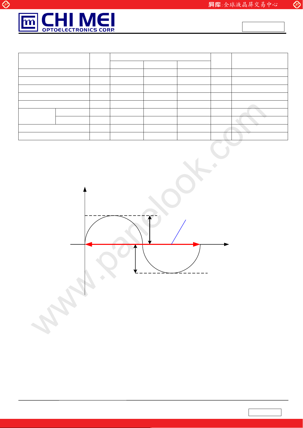
Note (3) Definition of Gray to Gray Switching Time :
100%
90%
Optical
Response
10%
0%
Gray to gray
switching time
25
Gray to gray
switching time
ime
The information described in this technical specification is tentative and it is possible to be changed without prior notice.
Please contact CMO ’s representative while your product design is based on this specification.
Version 1.0
One step solution for LCD / PDP / OLED panel application: Datasheet, inventory and accessory!
www.panelook.com
Page 26

Global LCD Panel Exchange Center
A
A
(
)
A
(
)
A
(
)
www.panelook.com
The driving signal means the signal of gray level 0, 63, 127, 191, 255.
Gray to gray average time means the average switching time of gray level 0 ,63,127,191,255 to each
other .
, L
Note (4) Definition of Luminance of White (L
):
C
AVE
Measure the luminance of gray level 255 at center point and 5 points
L
= L (5)
C
L
= [L (1)+ L (2)+ L (3)+ L (4)+ L (5)] / 5
AVE
where L (x) is corresponding to the luminance of the point X at the figure in Note (7).
Note (5) Definition of Cross Talk (CT):
Issued Date: Oct. 29, 2008
Model No.: V400H1 - L04
Preliminary
CT = | Y
– YA | / YA× 100 (%)
B
Where:
(a)
Y
= Luminance of measured location without gray level 255 pattern (cd/m2)
A
Y
= Luminance of measured location with gray level 255 pattern (cd/m2)
B
(0, 0)
Y
(D/8,W/2)
A, L
Y
(D/2,7W/8)
A, D
(b)
Y
= Luminance of measured location without gray level 255 pattern (cd/m2)
A
Y
= Luminance of measured location with gray level 255 pattern (cd/m2)
B
ctive Area
Gray 51
Y
A, U
Y
A, R
(D,W)
(D/2,W/8)
(7D/8,W/2)
(D/4,W/4)
Y
(D/8,W/2)
B, L
Y
(D/2,7W/8)
B, D
(0, 0)
ctive Area
Gray 0
Gray 255
Gray 51
Y
(D/2,W/8)
B, U
Y
(7D/8,W/2)
B, R
(3D/4,3W/4)
D,W
Y
(D/8,W/2)
A, L
Y
(D/2,7W/8)
A, D
(0, 0)
ctive Area
Gray 0
Y
Y
D,W
A, U
A, R
(D/2,W/8)
(7D/8,W/2)
26
(D/4,W/4)
Y
(D/8,W/2)
B, L
Y
(D/2,7W/8)
B, D
(0, 0)
ctive Area
Gray 0
Gray 255
Gray 0
The information described in this technical specification is tentative and it is possible to be changed without prior notice.
Please contact CMO ’s representative while your product design is based on this specification.
One step solution for LCD / PDP / OLED panel application: Datasheet, inventory and accessory!
Y
(D/2,W/8)
B, U
Y
(7D/8,W/2)
B, R
(3D/4,3W/4)
D,W
Version 1.0
www.panelook.com
Page 27

Global LCD Panel Exchange Center
Note (6) Measurement Setup:
The LCD module should be stabilized at given temperature for 1 hour to avoid abrupt temperature
change during measuring. In order to stabilize the luminance, the measurement should be
executed after lighting Backlight for 1 hour in a windless room.
LCD Module
LCD Panel
www.panelook.com
Issued Date: Oct. 29, 2008
Model No.: V400H1 - L04
Preliminary
Center of the Screen
Note (7) Definition of White Variation (δW):
Measure the luminance of gray level 255 at 5 points
δW = Maximum [L (1), L (2), L (3), L (4), L (5)] / Minimum [L (1), L (2), L (3), L (4), L (5)]
Display Color Analyzer
(Minolta CA210)
Light Shield Room
(Ambient Luminance < 2 lux)
Horizontal Line
D
D/4 D/2 3D/4
12
: Test Point
5
X
X=1 to 5
W
W/4
W/2
Vertical Line
3W/4
The information described in this technical specification is tentative and it is possible to be changed without prior notice.
Please contact CMO ’s representative while your product design is based on this specification.
One step solution for LCD / PDP / OLED panel application: Datasheet, inventory and accessory!
34
Active Area
27
Version 1.0
www.panelook.com
Page 28

Global LCD Panel Exchange Center
8. DEFINITION OF LABELS
8.1 CMO MODULE LABEL
The barcode nameplate is pasted on each module as illustration, and its definitions are as following explanation.
www.panelook.com
Issued Date: Oct. 29, 2008
Model No.: V400H1 - L04
Preliminary
CHI MEI
OPTOELECTRONICS
(a) Model Name: V400H1-L04
(b) Revision: Rev. XX, for example: A0, A1… B1, B2… or C1, C2…etc.
(c) Serial ID: XX-XX-X-XX-YMD-L-NNNN
Code Meaning Description
XX CMO internal use XX Revision Cover all the change
X CMO internal use -
XX CMO internal use -
Year, month, day
YMD
L Product line # Line 1=1, Line 2=2, Line 3=3, …
NNNN Serial number Manufacturing sequence of product
V400H1 -L04 Rev. XX
X X X X X X X Y M D L N N N N
Year: 2001=1, 2002=2, 2003=3, 2004=4…
Month: Jan. ~ Dec.=1, 2, 3, ~, 9, A, B, C
st
Day: 1
to 31st =1, 2, 3, ~, 9, A, B, C, ~, W, X, Y, exclude I, O, and U
E207943
MADE IN TAIWAN
28
The information described in this technical specification is tentative and it is possible to be changed without prior notice.
Please contact CMO ’s representative while your product design is based on this specification.
One step solution for LCD / PDP / OLED panel application: Datasheet, inventory and accessory!
Version 1.0
www.panelook.com
Page 29

Global LCD Panel Exchange Center
9. PACKAGING
9.1 PACKING SPECIFICATIONS
(1) 4 LCD TV modules / 1 Box
(2) Box dimensionsΚ1040(L) X 310 (W) X 640(H)
(3) WeightΚapproximately 47Kg ( 4 modules per box)
9.2 PACKING METHOD
Figures 9-1 and 9-2 are the packing method
www.panelook.com
Issued Date: Oct. 29, 2008
Model No.: V400H1 - L04
Preliminary
LCD TV Module
Anti-static Bag
Cushion(Top)
Figure.9-1 packing method
29
The information described in this technical specification is tentative and it is possible to be changed without prior notice.
Please contact CMO ’s representative while your product design is based on this specification.
One step solution for LCD / PDP / OLED panel application: Datasheet, inventory and accessory!
Version 1.0
www.panelook.com
Page 30

Global LCD Panel Exchange Center
Sea / Land Transportation (40ft Container)
www.panelook.com
Issued Date: Oct. 29, 2008
Model No.: V400H1 - L04
Preliminary
(Pallet:L1250*W1050*H140mm)
Air Transportation
(Pallet:L1250*W1050*H140mm)
Figure. 9-2 Packing method
30
The information described in this technical specification is tentative and it is possible to be changed without prior notice.
Please contact CMO ’s representative while your product design is based on this specification.
One step solution for LCD / PDP / OLED panel application: Datasheet, inventory and accessory!
Version 1.0
www.panelook.com
Page 31

Global LCD Panel Exchange Center
www.panelook.com
Issued Date: Oct. 29, 2008
Model No.: V400H1 - L04
Preliminary
10. PRECAUTIONS
10.1 ASSEMBLY AND HANDLING PRECAUTIONS
(1) Do not apply rough force such as bending or twisting to the module during assembly.
(2) It is recommended to assemble or to install a module into the user’s system in clean working areas.
The dust and oil may cause electrical short or worsen the polarizer.
(3) Do not apply pressure or impulse to the module to prevent the damage of LCD panel and backlight.
(4) Always follow the correct power-on sequence when the LCD module is turned on. This can prevent the
damage and latch-up of the CMOS LSI chips.
(5) Do not plug in or pull out the I/F connector while the module is in operation.
(6) Do not disassemble the module.
(7) Use a soft dry cloth without chemicals for cleaning, because the surface of polarizer is very soft and
easily scratched.
(8) Moisture can easily penetrate into LCD module and may cause the damage during operation.
(9) High temperature or humidity may deteriorate the performance of LCD module. Please store LCD
modules in the specified storage conditions.
(10) When ambient temperature is lower than 10ºC, the display quality might be reduced. For example, the
response time will become slow, and the starting voltage of CCFL will be higher than that of room
temperature.
10.2 SAFETY PRECAUTIONS
(1) The startup voltage of a backlight is over 1000 Volts. It may cause an electrical shock while assembling
with the inverter. Do not disassemble the module or insert anything into the backlight unit.
(2) If the liquid crystal material leaks from the panel, it should be kept away from the eyes or mouth. In
case of contact with hands, skin or clothes, it has to be washed away thoroughly with soap.
(3) After the module’s end of life, it is not harmful in case of normal operation and storage.
10.3 SAFETY STANDARDS
The LCD module should be certified with safety regulations as follows:
(1) UL60950-1 or updated standard.
(2) IEC60950-1 or updated standard.
(3) UL60065 or updated standard.
(4) IEC60065 or updated standard.
31
The information described in this technical specification is tentative and it is possible to be changed without prior notice.
Please contact CMO ’s representative while your product design is based on this specification.
One step solution for LCD / PDP / OLED panel application: Datasheet, inventory and accessory!
Version 1.0
www.panelook.com
Page 32

Global LCD Panel Exchange Center
9. MECHANICAL CHARACTERISTICS
www.panelook.com
Issued Date: Oct. 29, 2008
Model No.: V400H1 - L04
Preliminary
ڻႝηިҽԖϦљ
CHI MEI
32
The information described in this technical specification is tentative and it is possible to be changed without prior notice.
Please contact CMO ’s representative while your product design is based on this specification.
One step solution for LCD / PDP / OLED panel application: Datasheet, inventory and accessory!
Version 1.0
www.panelook.com
Page 33

Global LCD Panel Exchange Center
www.panelook.com
Issued Date: Oct. 29, 2008
Model No.: V400H1 - L04
Preliminary
ڻႝηިҽԖϦљ
CHI MEI
33
The information described in this technical specification is tentative and it is possible to be changed without prior notice.
Please contact CMO ’s representative while your product design is based on this specification.
One step solution for LCD / PDP / OLED panel application: Datasheet, inventory and accessory!
Version 1.0
www.panelook.com
 Loading...