

Page 1

Global LCD Panel Exchange Center
MODEL NO.: V370H4
www.panelook.com
PRODUCT SPECIFICATION
ϭʳ Tentative Specification
ϭʳ Preliminary Specification
Ϯʳ Approval Specification
SUFFIX: LE2
Customer:
APPROVED BY SIGNATURE
Name / Title
Note
Please return 1 copy for your confirmation with your
signature and comments.
Approved By Checked By Prepared By
Chao-Chun Chung Vincent Chou WJ Chang
Version 2.0 1 DateΚΚΚΚ13 Aug. 2010
The copyright belongs to CHIMEI InnoLux. Any unauthorized use is prohibited
One step solution for LCD / PDP / OLED panel application: Datasheet, inventory and accessory!
www.panelook.com
Page 2
Global LCD Panel Exchange Center
www.panelook.com
PRODUCT SPECIFICATION
CONTENTS
1. GENERAL DESCRIPTION ............................................................................................................................................ 5
1.1 OVERVIEW ..........................................................................................................................................................5
1.2 FEATURES ..........................................................................................................................................................5
1.3 APPLICATION...................................................................................................................................................... 5
1.4 GENERAL SPECIFICATIONS .............................................................................................................................5
1.5 MECHANICAL SPECIFICATION .........................................................................................................................6
2. ABSOLUTE MAXIMUM RATINGS ................................................................................................................................7
2.1 ABSOLUTE RATINGS OF ENVIRONMENT........................................................................................................7
2.2 PACKAGE STORAGE.......................................................................................................................................... 8
2.3 ELECTRICAL ABSOLUTE RATINGS .................................................................................................................. 8
2.3.1 TFT LCD MODULE ....................................................................................................................................8
2.3.2 BACKLIGHT CONVERTER UNIT.............................................................................................................. 8
3. ELECTRICAL CHARACTERISTICS .............................................................................................................................9
3.1 TFT LCD MODULE ..............................................................................................................................................9
3.2 BACKLIGHT UNIT.............................................................................................................................................. 12
3.2.1 LED LIGHT BARCHARACTERISTICS (Ta = 25 ± 2 ºC)..........................................................................12
3.2.2 CONVERTER CHARACTERISTICS (Ta = 25 ± 2 ºC) .............................................................................12
3.2.3 CONVERTER INTERFACE CHARACTERISTICS ..................................................................................13
4. BLOCK DIAGRAM OF INTERFACE ...........................................................................................................................15
4.1 TFT LCD MODULE ............................................................................................................................................15
5. INPUT TERMINAL PIN ASSIGNMENT ....................................................................................................................... 16
5.1 TFT LCD Module Input CNF1 Connector Pin Assignment (GS13512-1411S-7F(Foxconn))............................. 16
5.2 BACKLIGHT UNIT.............................................................................................................................................. 18
5.3 DRIVING BOARD UNIT .....................................................................................................................................18
5.3 BLOCK DIAGRAM OF INTERFACE.................................................................................................................. 20
5.4 LVDS INTERFACE ............................................................................................................................................. 21
5.5 COLOR DATA INPUT ASSIGNMENT ................................................................................................................ 23
6. INTERFACE TIMING................................................................................................................................................... 24
6.1 INPUT SIGNAL TIMING SPECIFICATIONS...................................................................................................... 24
6.2 POWER ON/OFF SEQUENCE.......................................................................................................................... 27
7. OPTICAL CHARACTERISTICS ..................................................................................................................................28
Version 2.0 2 DateΚΚΚΚ13 Aug. 2010
The copyright belongs to CHIMEI InnoLux. Any unauthorized use is prohibited
One step solution for LCD / PDP / OLED panel application: Datasheet, inventory and accessory!
www.panelook.com
Page 3

Global LCD Panel Exchange Center
www.panelook.com
PRODUCT SPECIFICATION
7.1 TEST CONDITIONS........................................................................................................................................... 28
7.2 OPTICAL SPECIFICATIONS .............................................................................................................................29
8. PRECAUTIONS........................................................................................................................................................... 32
8.1 ASSEMBLY AND HANDLING PRECAUTIONS .................................................................................................32
8.2 SAFETY PRECAUTIONS ..................................................................................................................................32
9. DEFINITION OF LABELS............................................................................................................................................ 33
9.1 CMI MODULE LABEL ........................................................................................................................................33
10. PACKAGING..............................................................................................................................................................34
10.1 PACKING SPECIFICATIONS...........................................................................................................................34
10.2 PACKING METHOD......................................................................................................................................... 34
11. MECHANICAL CHARACTERISTICS ........................................................................................................................ 36
Version 2.0 3 DateΚΚΚΚ13 Aug. 2010
The copyright belongs to CHIMEI InnoLux. Any unauthorized use is prohibited
One step solution for LCD / PDP / OLED panel application: Datasheet, inventory and accessory!
www.panelook.com
Page 4
Global LCD Panel Exchange Center
Version Date
Ver. 2.0 Aug. 13 .2010 All All The Approval Specification was first issued.
Page
(New)
www.panelook.com
PRODUCT SPECIFICATION
REVISION HISTORY
Section Description
Version 2.0 4 DateΚΚΚΚ13 Aug. 2010
The copyright belongs to CHIMEI InnoLux. Any unauthorized use is prohibited
One step solution for LCD / PDP / OLED panel application: Datasheet, inventory and accessory!
www.panelook.com
Page 5
Global LCD Panel Exchange Center
1. GENERAL DESCRIPTION
1.1 OVERVIEW
V370H4-LE2 is a 37” TFT Liquid Crystal Display module with LED Backlight and 2ch-LVDS interface. This
module supports 1920 x 1080 Full HDTV format and can display true 16.7M colors (8bit). The converter module
for backlight is built-in.
1.2 FEATURES
Ё High brightness (450 nits)
Ё High contrast ratio (6000:1)
Ё Fast response time (Gray to gray average 8.5 ms)
Ё High color saturation (NTSC 72%)
Ё Full HDTV (1920 x 1080 pixels) resolution, true HDTV format
Ё DE (Data Enable) only mode
www.panelook.com
PRODUCT SPECIFICATION
Ё LVDS (Low Voltage Differential Signaling) interface
Ё Optimized response time for 60Hz or 50Hz frame rate
Ё Ultra wide viewing angle : Super MVA technology
Ё RoHS compliance
1.3 APPLICATION
Ё Standard Living Room TVs.
Ё Public Display Application.
Ё Home Theater Application.
Ё MFM Application.
1.4 GENERAL SPECIFICATIONS
Item Specification Unit Note
Active Area 819.36 (H) x 460.89 (V) (37” diagonal) mm
Bezel Opening Area 826.4(H) x 468 (V) mm
Driver Element a-si TFT active matrix -
Pixel Number 1920 x R.G.B. x 1080 pixel
Pixel Pitch (Sub Pixel) 0.14225 (H) x 0.42675 (V) mm
Pixel Arrangement RGB vertical stripe -
Display Colors 16.7M color
Display Operation Mode Transmissive mode / Normally Black -
Surface Treatment
Anti-Glare Coating (Haze 11%)
Hard Coating (3H)
(1)
- (2)
Note (1) Please refer to the attached drawings in chapter 9 for more information about the front and back outlines.
Note (2) The spec. of the surface treatment is temporarily for this phase. CMI reserves the rights to change this
feature.
Version 2.0 5 DateΚΚΚΚ13 Aug. 2010
The copyright belongs to CHIMEI InnoLux. Any unauthorized use is prohibited
One step solution for LCD / PDP / OLED panel application: Datasheet, inventory and accessory!
www.panelook.com
Page 6
Global LCD Panel Exchange Center
www.panelook.com
PRODUCT SPECIFICATION
1.5 MECHANICAL SPECIFICATION
1.5 MECHANICAL SPECIFICATIONS
Item Min. Typ. Max. Unit Note
Horizontal(H) 861.2 862.4 863.6 mm
Vertical(V) 502.8 504 505.2 mm
Module Size
Note (1) Please refer to the attached drawings for more information of front and back outline dimensions.
Depth(D) 14 15.2 16.4 mm To rear
Depth(D)
Weight 5810 g
24.4 25.6 26.8
mm To converter
(1)
cover
Version 2.0 6 DateΚΚΚΚ13 Aug. 2010
The copyright belongs to CHIMEI InnoLux. Any unauthorized use is prohibited
One step solution for LCD / PDP / OLED panel application: Datasheet, inventory and accessory!
www.panelook.com
Page 7
Global LCD Panel Exchange Center
2. ABSOLUTE MAXIMUM RATINGS
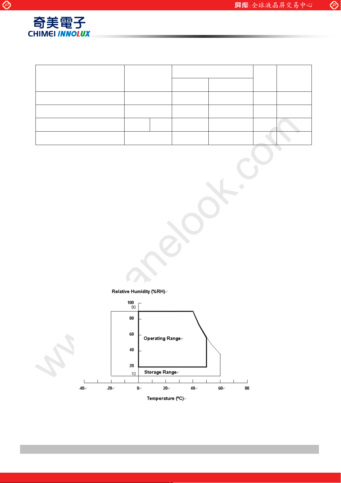
2.1 ABSOLUTE RATINGS OF ENVIRONMENT
Item Symbol
Storage Temperature TST -20 +60 ºC (1)
Operating Ambient Temperature TOP 0 50 ºC (1), (2)
www.panelook.com
PRODUCT SPECIFICATION
Value
Unit Note
Min. Max.
Shock (Non-Operating) SNOP
Vibration (Non-Operating) VNOP - 1.0 G (4), (5)
Note (1) Temperature and relative humidity range is shown in the figure below.
(a) 90 %RH Max. (Ta Љ 40 ºC).
(b) Wet-bulb temperature should be 39 ºC Max. (Ta > 40 ºC).
(c) No condensation.
Note (2) The maximum operating temperature is based on the test condition that the surface temperature of
display area is less than or equal to 65 ºC with LCD module alone in a temperature controlled chamber.
Thermal management should be considered in final product design to prevent the surface temperature of
display area from being over 65 ºC. The range of operating temperature may degrade in case of
improper thermal management in final product design.
Note (3) 11 ms, half sine wave, 1 time for ± X, ± Y, ± Z.
Note (4) 10 ~ 200 Hz, 10 min, 1 time each X, Y, Z.
Note (5) At testing Vibration and Shock, the fixture in holding the module has to be hard and rigid enough so that
the module would not be twisted or bent by the fixture.
X,Y,Z
axis
- 50 G (3), (5)
Version 2.0 7 DateΚΚΚΚ13 Aug. 2010
The copyright belongs to CHIMEI InnoLux. Any unauthorized use is prohibited
One step solution for LCD / PDP / OLED panel application: Datasheet, inventory and accessory!
www.panelook.com
Page 8
Global LCD Panel Exchange Center
2.2 PACKAGE STORAGE
When storing modules as spares for a long time, the following precaution is necessary.
(a) Do not leave the module in high temperature, and high humidity for a long time, It is highly recommended to
store the module with temperature from 0 to 35 к at normal humidity without condensation.
(b) The module shall be stroed in dark place. Do not store the TFT-LCD module in direct sunlight or fluorescent
light.
2.3 ELECTRICAL ABSOLUTE RATINGS
2.3.1 TFT LCD MODULE
Item Symbol
Power Supply Voltage VCC -0.3 13.5 V
Logic Input Voltage VIN -0.3 3.6 V
www.panelook.com
PRODUCT SPECIFICATION
Value
Unit Note
Min. Max.
(1)
2.3.2 BACKLIGHT CONVERTER UNIT
Item Symbol
Light Bar Voltage VW Ta = 25 к - - 60 V
Converter Input Voltage VBL - 0 - 30 V (1)
Control Signal Level - - -0.3 - 7 V (1),(3)
Note (1) Permanent damage to the device may occur if maximum value s are exceeded. Function operation
should be restricted to the conditions described under Normal Operating Conditions.
Note (2) No moisture condensation or freezing.
Note (3) The control signals include On/Off Control, Internal PWM Control and External PWM Control.
Tes t
Condition
Min. Type Max. Unit Note
DC
Version 2.0 8 DateΚΚΚΚ13 Aug. 2010
The copyright belongs to CHIMEI InnoLux. Any unauthorized use is prohibited
One step solution for LCD / PDP / OLED panel application: Datasheet, inventory and accessory!
www.panelook.com
Page 9
Global LCD Panel Exchange Center
3. ELECTRICAL CHARACTERISTICS
3.1 TFT LCD MODULE
(Ta = 25 ± 2 ºC)
Parameter Symbol
Power Supply Voltage VCC 10.8 12 13.2 V (1)
www.panelook.com
PRODUCT SPECIFICATION
Value
Unit Note
Min. Typ. Max.
Rush Current I
Power Supply Current
Differential Input High
Threshold Voltage
Differential Input Low
Threshold Voltage
LVDS
interface
Common Input Voltage VCM 1.0 1.2 1.4 V
Differential input voltage
Terminating Resistor R
CMOS
interface
Input High Threshold Voltage VIH 2.7 - 3.3 V
Input Low Threshold Voltage V
White Pattern
Horizontal Stripe
Black Pattern
(Single-end)
- - 2.8 A (2)
RUSH
-
-
-
V
LVTH
V
- - -100 mV
LVTL
|V
| 200 - 600 mV
ID
- 100 - ohm
T
0 - 0.7 V
IL
- 0.32 - A
- 0.55 0.66 A
- 0.31 - A
+100 - - mV
Note (1) The module should be always operated within the above ranges.
(3)
(4)
Version 2.0 9 DateΚΚΚΚ13 Aug. 2010
The copyright belongs to CHIMEI InnoLux. Any unauthorized use is prohibited
One step solution for LCD / PDP / OLED panel application: Datasheet, inventory and accessory!
www.panelook.com
Page 10
Global LCD Panel Exchange Center
Note (2) Measurement condition:
www.panelook.com
PRODUCT SPECIFICATION
GND
Vcc rising time is 470us
Vcc
0.9Vcc
0.1Vcc
470us
Version 2.0 10 DateΚΚΚΚ13 Aug. 2010
The copyright belongs to CHIMEI InnoLux. Any unauthorized use is prohibited
One step solution for LCD / PDP / OLED panel application: Datasheet, inventory and accessory!
www.panelook.com
Page 11
Global LCD Panel Exchange Center
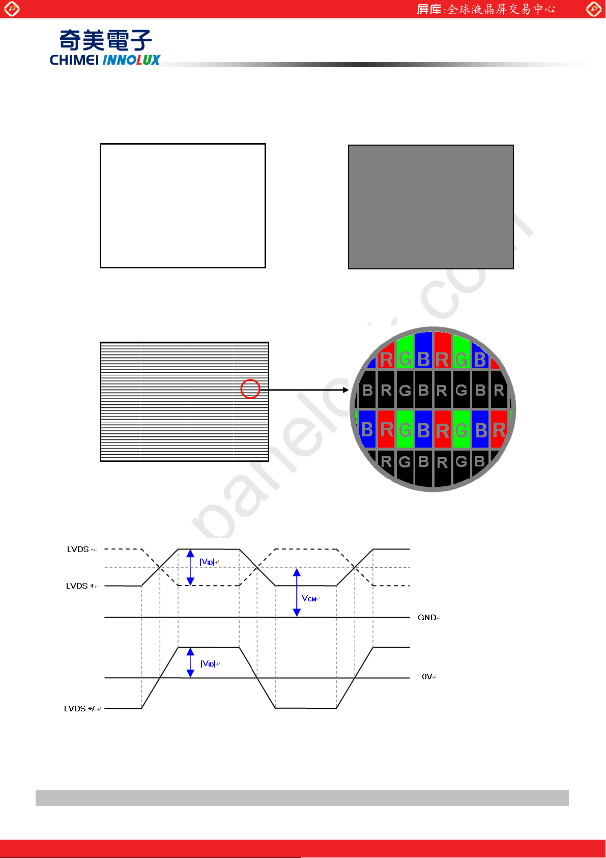
Note (3) The specified power supply current is under the conditions at Vcc = 12 V, Ta = 25 ± 2 ºC, fv = 60 Hz,
whereas a power dissipation check pattern below is displayed.
www.panelook.com
PRODUCT SPECIFICATION
a. White Pattern
Active Area
c. Horizontal Pattern
b. Black Pattern
Active Area
Note (4) The LVDS input characteristics are as follows:
Version 2.0 11 DateΚΚΚΚ13 Aug. 2010
The copyright belongs to CHIMEI InnoLux. Any unauthorized use is prohibited
One step solution for LCD / PDP / OLED panel application: Datasheet, inventory and accessory!
www.panelook.com
Page 12
Global LCD Panel Exchange Center
3.2 BACKLIGHT UNIT
3.2.1
LED LIGHT BARCHARACTERISTICS (
The backlight unit contains 1pcs light bar.
www.panelook.com
PRODUCT SPECIFICATION
Ta = 25 ± 2 ºC)
Parameter Symbol
Unit Note
Min. Typ. Max.
Value
Total Current (4 String) If
One String Current I
LED Forward Voltage V
One String Voltage V
One String Voltage Variation
ϦV
Life time -
L
f
W
W
- 480 508.8
- 120 127.2
3.0 3.25 3.5
36 - 42
- - 2
30,000 - -
mA
mA
I
V
DC
V
DC
L
I
L
V
Hrs (1)
Note (1) The lifetime is defined as the time which luminance of the LED decays to 50% compared to the
initial value, Operating condition: Continuous operating at Ta = 25±2 , Iк
=120mA
L
3.2.2 CONVERTER CHARACTERISTICS (Ta = 25 ± 2 ºC)
Value
Parameter Symbol
Unit Note
Min. Typ. Max.
Power Consumption PBL - 83 96 W (1),(2) IL =120mA
=120mA
=120mA
Converter Input Voltage
VBL 22.8 24.0 25.2 VDC
Converter Input Current IBL - 3.46 4 A Non Dimming
=24V, (IL=typ.)
V
Input Inrush Current - - - 6.2 Apeak
BL
(3)
Input Rush current - - - 5.4 A (3)
Dimming Frequency FB 150 160 170 Hz
Minimum Duty Ratio D
5 10
MIN
- %
(4)
Note (1) The power supply capacity should be higher than the total converter power consumption PBL. Since the
pulse width modulation (PWM) mode was applied for backlight dimming, the driving current changed as
PWM duty on and off. The transient response of power supply should be considered for the changing
loading when converter dimming.
Note (2) The measurement condition of Max. value is based on 37" backlight unit under input voltage 24V,
average LED current 127.2 mA and lighting 1 hour later.
Note (3) The duration of Input Rush Current is about 30ms.
Note (4) 5% minimum duty ratio is only valid for electrical operation.
Version 2.0 12 DateΚΚΚΚ13 Aug. 2010
The copyright belongs to CHIMEI InnoLux. Any unauthorized use is prohibited
One step solution for LCD / PDP / OLED panel application: Datasheet, inventory and accessory!
www.panelook.com
Page 13
Global LCD Panel Exchange Center
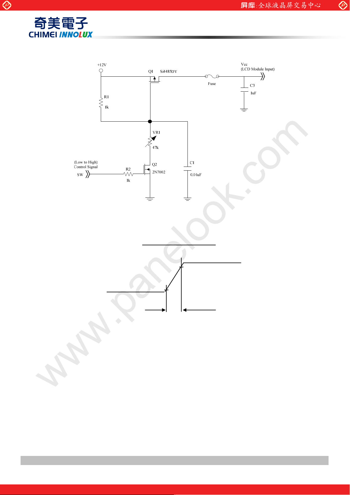
3.2.3 CONVERTER INTERFACE CHARACTERISTICS
External dimming: 150Hz~170Hz, duty ratio: 10%~100%
www.panelook.com
PRODUCT SPECIFICATION
Parameter Symbol
ON
On/Off Control Voltage
OFF
Internal PWM Control
Voltage
External PWM Control
Voltage
Status Signal
VBL Rising Time Tr1
Control Signal Rising Time Tr
Control Signal Falling Time Tf
MAX
MIN
LO
LO
VBLON
VIPWM
HI
VEPWM
HI
Status
0
0
0
30
Value
Ё
Ё
Ё
0
Ё
Ё
Ё
ЁЁ
Tes t
Condition
Ё
Ё
Ё
ЁЁ
Ё
Ё
Ё
Ё
Ё
ЁЁЁ
ЁЁЁ
Min. Typ. Max.
2.0
3.15
2.0
3.0 3.3 3.6 V Normal
Unit Note
5.0 V
0.8 V
3.45
Ё
5.0 V Duty on
0.8 V Duty off
0.8 V Abnormal
100 ms
100 ms
V maximum duty ratio
V minimum duty ratio
ms 10%-90%V
BL
PWM Signal Rising Time TPWMR
PWM Signal Falling Time TPWMF
Input Impedance Rin
PWM Delay Time TPWM
T
BLON Delay Time
BLON Off Time Toff
Note (1) The Dimming signal should be valid before backlight turns on by BLON signal. It is inhibited to
change the internal/external PWM signal during backlight turn on period.
Note (2) The power sequence and control signal timing are shown in the following figure. For a certain
reason, the converter has a possibility to be damaged with wrong power sequence and control
signal timing.
Note (3) While system is turned ON or OFF, the power sequences must follow as below descriptions:
Turn ON sequence: VBL → PWM signal → BLON
on
T
on1
ЁЁЁ
ЁЁЁ
Ё
Ё
Ё
Ё
Ё
1
100
300
300
300
ЁЁ
ЁЁ
ЁЁ
ЁЁ
ЁЁ
50 us
50 us
MΩ
ms
ms
ms
ms
Turn OFF sequence: BLOFF → PWM signal → VBL
Version 2.0 13 DateΚΚΚΚ13 Aug. 2010
The copyright belongs to CHIMEI InnoLux. Any unauthorized use is prohibited
One step solution for LCD / PDP / OLED panel application: Datasheet, inventory and accessory!
www.panelook.com
Page 14
Global LCD Panel Exchange Center
www.panelook.com
PRODUCT SPECIFICATION
V
V
V
BL
V
BLON
EPWM
IPWM
9
Toff
%/
Tf1
9
%/
Tr1
9
%/
9
%/
2.0V
0.8V
Ton
Ton1
0
0
Backlight on duration
Tr
Tf
Ext. Dimming Function
T
PWMR
2.0V
0
0.8V
T
PWM
T
PWMF
Floating
3.3V
0
Floating
Int. Dimming Function
V
W
External
PWM
Period
External
PWM Duty
100%
Minimun
Duty
Version 2.0 14 DateΚΚΚΚ13 Aug. 2010
The copyright belongs to CHIMEI InnoLux. Any unauthorized use is prohibited
One step solution for LCD / PDP / OLED panel application: Datasheet, inventory and accessory!
www.panelook.com
Page 15
Global LCD Panel Exchange Center
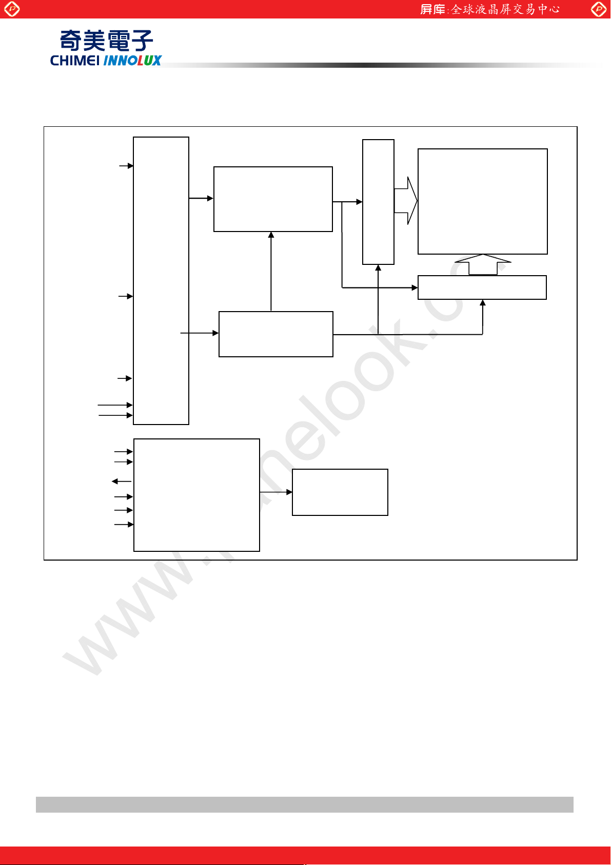
4. BLOCK DIAGRAM OF INTERFACE
4.1 TFT LCD MODULE
ERX0(+/-)
ERX1(+/-)
ERX2(+/-)
ERX3(+/-)
ECLK(+/-)
Foxconn, GS13512-1411S-7F or equivalent
INPUT CONNECTOR
ORX0(+/-)
ORX1(+/-)
ORX2(+/-)
ORX3(+/-)
OCLK(+/-)
www.panelook.com
PRODUCT SPECIFICATION
TIMING
CONTROLLER
DC/DC CONVERTER
SCAN DRIVER
TFT LCD PANEL
(1920x3x1080)
DATA DRIVER
SELLVDS
Vcc
GND
VBL
GND
Status
E_PWM
I_PWM
BLON
CONVERTER
CONNECTOR
CN1: CI0114M1HR0-LA
(CvilLux)
or equivalent
CN2 ~ CN5: 161035-10041-3 (P-TWO)
or equivalent
BACKLIGHT
UNIT
Version 2.0 15 DateΚΚΚΚ13 Aug. 2010
The copyright belongs to CHIMEI InnoLux. Any unauthorized use is prohibited
One step solution for LCD / PDP / OLED panel application: Datasheet, inventory and accessory!
www.panelook.com
Page 16
Global LCD Panel Exchange Center
www.panelook.com
PRODUCT SPECIFICATION
5. INPUT TERMINAL PIN ASSIGNMENT
5.1 TFT LCD Module Input CNF1 Connector Pin Assignment (GS13512-1411S-7F(Foxconn))
Pin Name Description Note
1 GND Ground
N.C. No Connection
2
N.C. No Connection
3
N.C. No Connection
4
N.C. No Connection
5
N.C. No Connection
6
7 SELLVDS LVDS data format Selection (3)(4)
N.C. No Connection
8
9 N.C. No Connection
N.C. No Connection
10
GND Ground
11
12 ERX0- Even pixel Negative LVDS differential data input. Channel 0
13 ERX0+ Even pixel Positive LVDS differential data input. Channel 0
14 ERX1- Even pixel Negative LVDS differential data input. Channel 1
15 ERX1+ Even pixel Positive LVDS differential data input. Channel 1
16 ERX2- Even pixel Negative LVDS differential data input. Channel 2
17 ERX2+ Even pixel Positive LVDS differential data input. Channel 2
18 GND Ground
19 ECLK- Even pixel Negative LVDS differential clock input
20 ECLK+ Even pixel Positive LVDS differential clock input
21 GND Ground
22 ERX3- Even pixel Negative LVDS differential data input. Channel 3
23 ERX3+ Even pixel Positive LVDS differential data input. Channel 3
N.C. No Connection
24
N.C. No Connection
25
GND Ground
26
GND Ground
27
28 ORX0- Odd pixel Negative LVDS differential data input. Channel 0
29 ORX0+ Odd pixel Positive LVDS differential data input. Channel 0
30 ORX1- Odd pixel Negative LVDS differential data input. Channel 1
31 ORX1+ Odd pixel Positive LVDS differential data input. Channel 1
32 ORX2- Odd pixel Negative LVDS differential data input. Channel 2
33 ORX2+ Odd pixel Positive LVDS differential data input. Channel 2
34 GND Ground
35 OCLK- Odd pixel Negative LVDS differential clock input.
36 OCLK+ Odd pixel Positive LVDS differential clock input.
37 GND Ground
38 ORX3- Odd pixel Negative LVDS differential data input. Channel 3
39 ORX3+ Odd pixel Positive LVDS differential data input. Channel 3
N.C. No Connection
40
N.C. No Connection
41
GND Ground
42
GND Ground
43
GND Ground
44
GND Ground
45
GND Ground
46
N.C. No Connection
47
48 VCC +12V power supply
49 VCC +12V power supply
50 VCC +12V power supply
51 VCC +12V power supply
(2)
(2)
(5)
(5)
(5)
(2)
(5)
(5)
(5)
(2)
(2)
Version 2.0 16 DateΚΚΚΚ13 Aug. 2010
The copyright belongs to CHIMEI InnoLux. Any unauthorized use is prohibited
One step solution for LCD / PDP / OLED panel application: Datasheet, inventory and accessory!
www.panelook.com
Page 17
Global LCD Panel Exchange Center
g
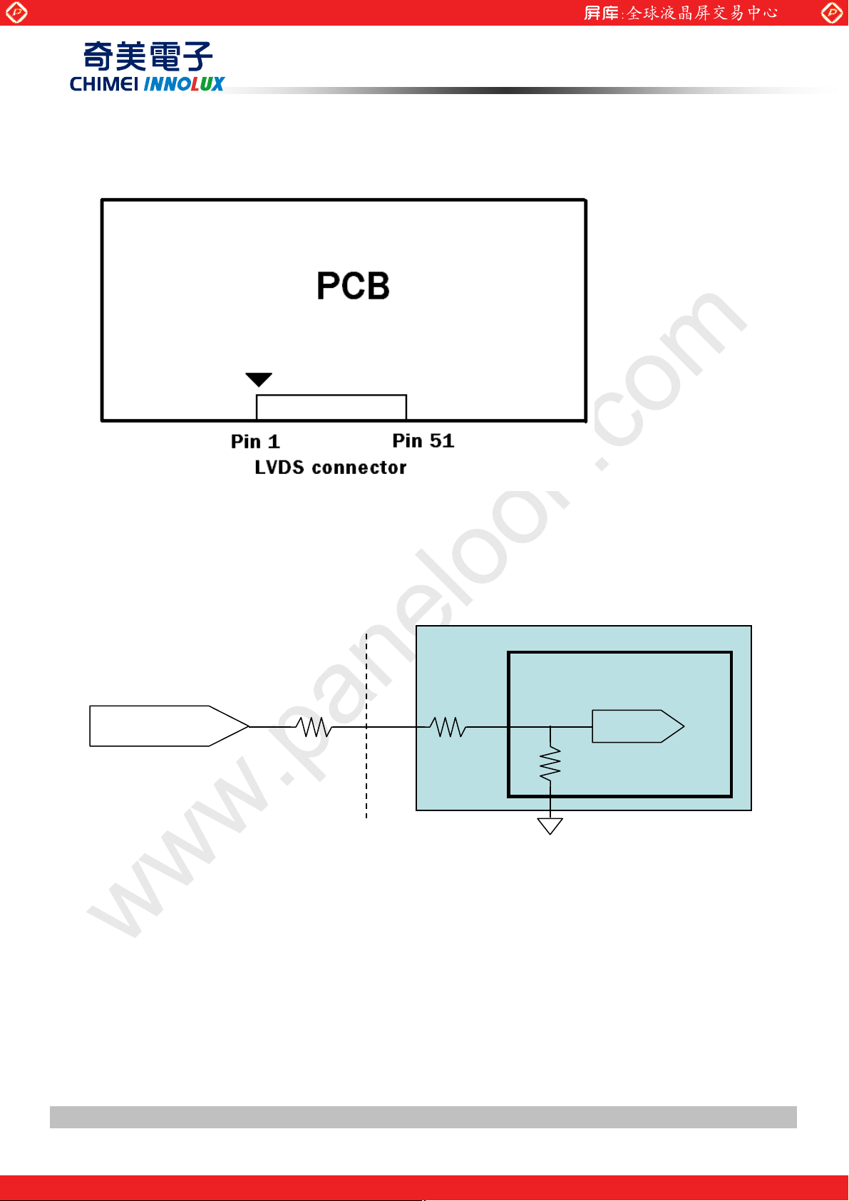
Note (1) LVDS connector pin orderdefined as follows
www.panelook.com
PRODUCT SPECIFICATION
Note (2) Reserved for internal use. Please leave it open.
Note (3) Low = Open or connect to GND: VESA Format, High = Connect to +3.3V: JEIDA Format.
Note (4) LVDS signal pin connected to the LCM side has the following diagram.
R1 in the system side should be less than 1K Ohm. (R1 < 1K Ohm)
TCON
R1
Selector (pin7)
System side
R2
Settin
LCM side
System side: R1 < 1K
Note (5) Two pixel data send into the module for every clock cycle. The first pixel of the frame is odd pixel and
the second pixel is even pixel.
Version 2.0 17 DateΚΚΚΚ13 Aug. 2010
The copyright belongs to CHIMEI InnoLux. Any unauthorized use is prohibited
One step solution for LCD / PDP / OLED panel application: Datasheet, inventory and accessory!
www.panelook.com
Page 18
Global LCD Panel Exchange Center
5.2 BACKLIGHT UNIT
The pin configuration for the housing and the leader wire is shown in the table below.
CN2, 5 : 161035-10041-3 (P-TWO) or 7083K-F10N-04L(E&T) or
Pin № Symbol Feature NOTE
1 VLED
2 VLED
3 NC
4 NC
5 NC
6 NC
7 N1
8 N2
9 N3
10 N4
www.panelook.com
PRODUCT SPECIFICATION
equivalent
Positive of LED String
No Connection
Negative of LED String
Note (1) The backlight interface housing for high voltage side is a model
P-TWO or equivalent.
5.3 DRIVING BOARD UNIT
CN1: CI0114M1HR0-LA (CvilLux) or equivalent
Pin № Signal name Feature
1
2
3
4
5
6
7
8
9
10
11 Status
12 E_PWM External PWM Control
13 I_PWM Internal PWM Control
V
BL
GND GND
+24 V
Normal (3.3V)
Abnormal (0V)
161035-10041-3
, manufactured by
14 BLON BL ON/OFF
Version 2.0 18 DateΚΚΚΚ13 Aug. 2010
The copyright belongs to CHIMEI InnoLux. Any unauthorized use is prohibited
One step solution for LCD / PDP / OLED panel application: Datasheet, inventory and accessory!
www.panelook.com
Page 19

Global LCD Panel Exchange Center
CN2 ~ CN5 : 161035-10041-3 (P-TWO) or 7083K-F10N-04L(E&T) or
Pin № Symbol Feature NOTE
1 N4
2 N3
3 N2
4 N1
5 NC
6 NC
7 NC
8 NC
9 VLED
10 VLED
www.panelook.com
PRODUCT SPECIFICATION
equivalent
Negative of LED String
No Connection
Positive of LED String
Version 2.0 19 DateΚΚΚΚ13 Aug. 2010
The copyright belongs to CHIMEI InnoLux. Any unauthorized use is prohibited
One step solution for LCD / PDP / OLED panel application: Datasheet, inventory and accessory!
www.panelook.com
Page 20
Global LCD Panel Exchange Center
G0-EG
G0-EG
0
r
p
ORx0
p
CLK
OB0
K
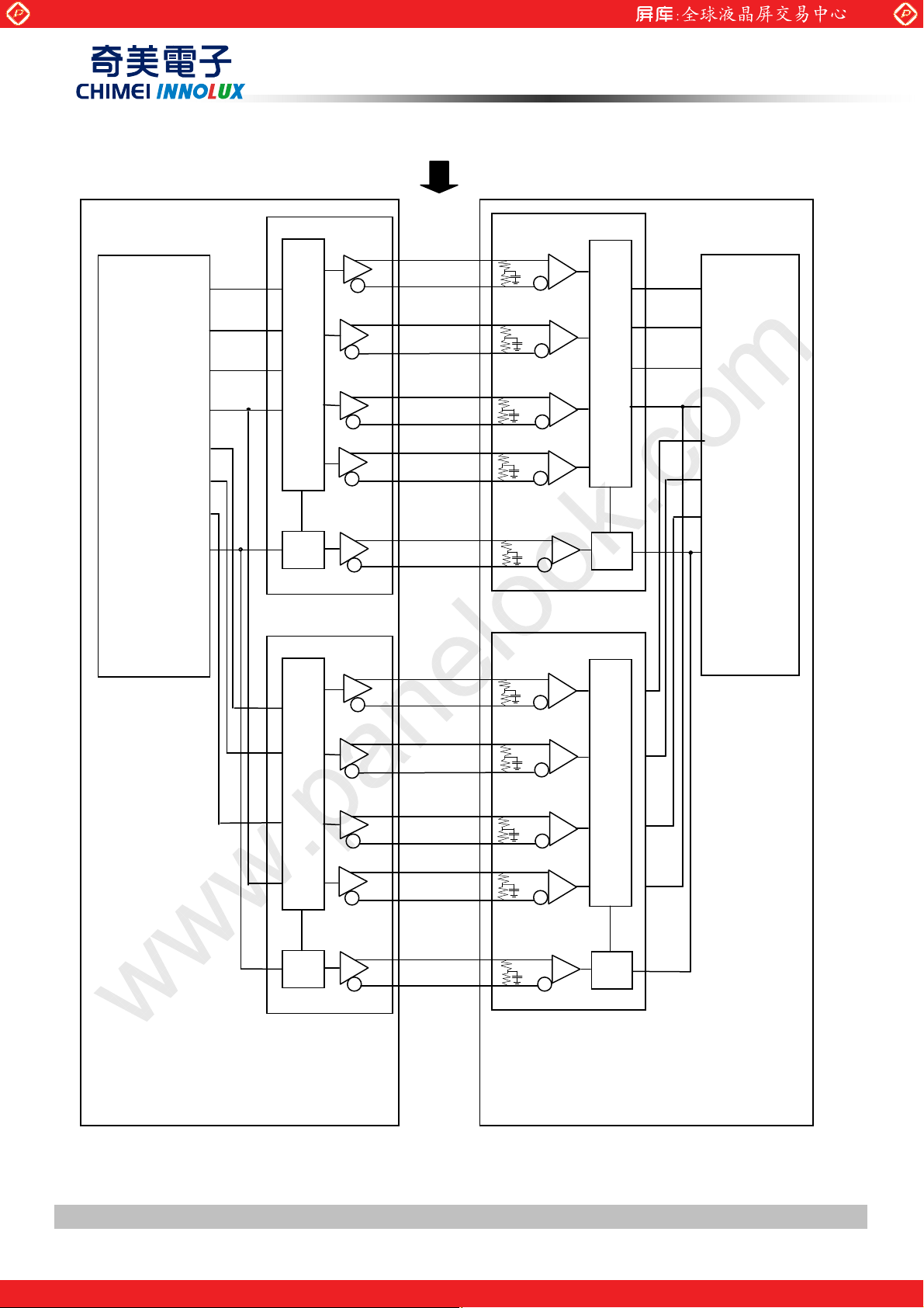
5.3 BLOCK DIAGRAM OF INTERFACE
www.panelook.com
PRODUCT SPECIFICATION
ER0-ER7
E
EB0-EB7
DE
OR0-OR7
OG0-OG7
OB0-OB7
D
Host
Graphics
Controller
ERx0+
TxIN
ERx0-
ERx1+
7
ERx1-
ERx2+
ERx2-
ERx3+
ERx3-
51
51
51
51
51
51
51
51
Ө
100pF
Ө
Ө
100
Ө
Ө
100pF
Ө
Ө
100pF
Ө
RxOUT
ER0-ER7
F
E
EB
7
-EB7
DE
OR0-OR7
OG0-OG7
-OB7
ECLK+
PLL
51
Ө
51
100pF
Ө
-
PLL
DCL
Timing
ORx0+
-
ORx1+
ORx1-
51
51
51
Ө
100pF
Ө
Ө
100
F
Controlle
ORx2+
ORx2-
ORx3+
ORx3-
OCLK+
PLL
LVDS Transmitter
51
Ө
51
51
51
51
51
100pF
Ө
Ө
100pF
Ө
Ө
100pF
Ө
-
LVDS Receiver
PLL
THC63LVDM83A
(LVDF83A)
Version 2.0 20 DateΚΚΚΚ13 Aug. 2010
The copyright belongs to CHIMEI InnoLux. Any unauthorized use is prohibited
One step solution for LCD / PDP / OLED panel application: Datasheet, inventory and accessory!
www.panelook.com
Page 21
Global LCD Panel Exchange Center
www.panelook.com
PRODUCT SPECIFICATION
ER0~ER7: Even pixel R data
EG0~EG7: Even pixel G data
EB0~EB7: Even pixel B data
OR0~OR7: Odd pixel R data
OG0~OG7: Odd pixel G data
OB0~OB7: Odd pixel B data
DE: Data enable signal
DCLK: Data clock signal
Notes (1) The system must have the transmitter to drive the module.
Notes (2) LVDS cable impedance shall be 50 ohms per signal line or about 100 ohms per twist-pair line when it is
used differentially
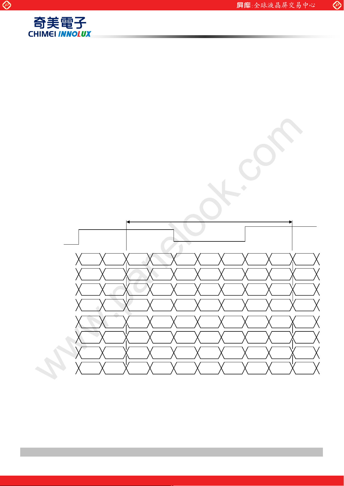
5.4 LVDS INTERFACE
VESA LVDS formatΚ(SELLVDS pin=L or open)
RXCLK
RXCLK
ORX0
ORX0
ORX1
ORX1
ORX2
ORX2
ORX3
ORX3
ERX0
ERX0
ERX1
ERX1
ERX2
ERX2
Current F\FOH
Current F\FOH
R5G0 R4 R3 R2 R1
R5G0 R4 R3 R2 R1
B0 G5B1
B0 G5B1
R5G0 R4 R3 R2 R1
R5G0 R4 R3 R2 R1
B0 G5B1
B0 G5B1
G3 G2G4
G3 G2G4
G3 G2G4
G3 G2G4
R0
R0
G1
G1
B2B4 B3B5VS HSDE
B2B4 B3B5VS HSDE
R6G6 R7G7B7 B6RSVD
R6G6 R7G7B7 B6RSVD
R0
R0
G1
G1
B2B4 B3B5VS HSDE
B2B4 B3B5VS HSDE
ERX3
ERX3
R6G6 R7G7B7 B6RSVD
R6G6 R7G7B7 B6RSVD
Version 2.0 21 DateΚΚΚΚ13 Aug. 2010
The copyright belongs to CHIMEI InnoLux. Any unauthorized use is prohibited
One step solution for LCD / PDP / OLED panel application: Datasheet, inventory and accessory!
www.panelook.com
Page 22
Global LCD Panel Exchange Center
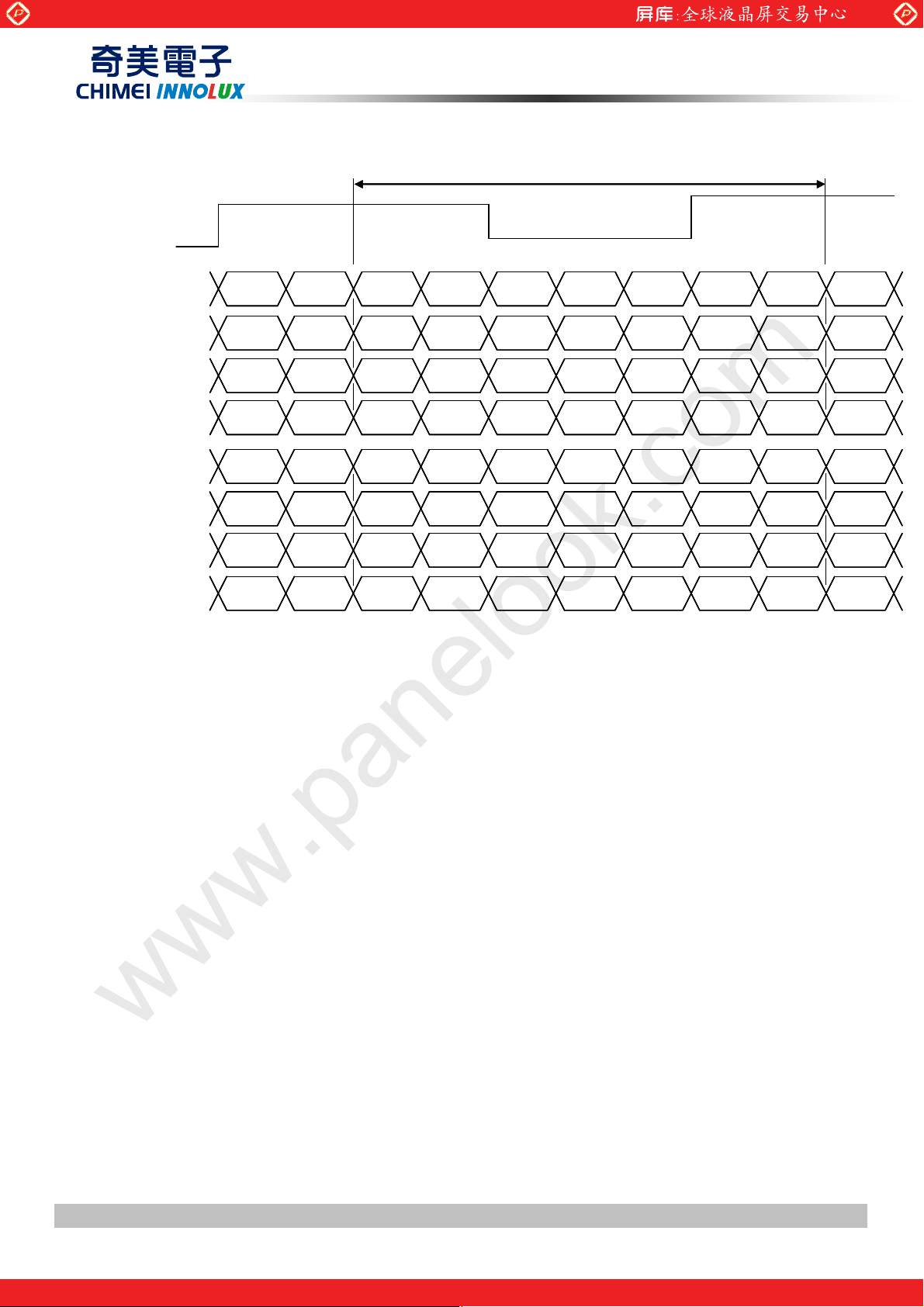
JEDIA LVDS formatΚ(SELLVDS pin=H)
RXCLK
RXCLK
www.panelook.com
PRODUCT SPECIFICATION
Current F\FOH
Current F\FOH
ORX0
ORX0
ORX1
ORX1
ORX2
ORX2
ORX3
ORX3
ERX0
ERX0
ERX1
ERX1
ERX2
ERX2
ERX3
ERX3
R0~R7: Pixel R Data (7; MSB, 0; LSB)
G0~G7: Pixel G Data (7; MSB, 0; LSB)
R7G2 R6 R5 R4 R3
R7G2 R6 R5 R4 R3
B2 G7B3
B2 G7B3
R7G2 R6 R5 R4 R3
R7G2 R6 R5 R4 R3
B2 G7B3
B2 G7B3
G5 G4G6
G5 G4G6
G5 G4G6
G5 G4G6
R2
R2
G3
G3
B4B6 B5B7VS HSDE
B4B6 B5B7VS HSDE
R0G0 R1G1B1 B0RSVD
R0G0 R1G1B1 B0RSVD
R2
R2
G3
G3
B4B6 B5B7VS HSDE
B4B6 B5B7VS HSDE
R0G0 R1G1B1 B0RSVD
R0G0 R1G1B1 B0RSVD
B0~B7: Pixel B Data (7; MSB, 0; LSB)
DE : Data enable signal
DCLK : Data clock signal
Notes: (1) RSVD (reserved) pins on the transmitter shall be “H” or “L”.
Version 2.0 22 DateΚΚΚΚ13 Aug. 2010
The copyright belongs to CHIMEI InnoLux. Any unauthorized use is prohibited
One step solution for LCD / PDP / OLED panel application: Datasheet, inventory and accessory!
www.panelook.com
Page 23

Global LCD Panel Exchange Center
5.5 COLOR DATA INPUT ASSIGNMENT
The brightness of each primary color (red, green and blue) is based on the 8-bit gray scale data input for the color.
The higher the binary input, the brighter the color. The table below provides the assignment of the color versus
data input.
Color
R7 R6 R5 R4 R3 R2 R1 R0 G7 G6 G5 G4 G3 G2 G1 G0 B7 B6 B5 B4 B3 B2 B1 B0
0
0
1
1
0
0
0
0
0
0
1
1
1
1
1
1
0
0
0
0
0
0
:
:
:
:
1
1
1
1
1
1
0
0
0
0
0
0
:
:
:
:
0
0
0
0
0
0
0
0
0
0
0
0
:
:
:
:
0
0
0
0
0
0
Basic
Colors
Gray
Scale
Of
Red
Gray
Scale
Of
Green
Gray
Scale
Of
Blue
Black
Red
Green
Blue
Cyan
Magenta
Yel lo w
White
Red (0) / Dark
Red (1)
Red (2)
:
:
Red (253)
Red (254)
Red (255)
Green (0) / Dark
Green (1)
Green (2)
:
:
Green (253)
Green (254)
Green (255)
Blue (0) / Dark
Blue (1)
Blue (2)
:
:
Blue (253)
Blue (254)
Blue (255)
www.panelook.com
PRODUCT SPECIFICATION
Data Signal
Red Green Blue
0
0
0
0
0
0
0
0
0
0
0
0
0
0
0
0
0
0
0
0
0
0
0
0
0
0
0
0
0
0
0
0
0
0
0
0
0
0
1
1
1
1
1
1
0
0
0
0
0
0
0
0
1
1
1
1
1
1
1
1
0
0
0
0
0
0
1
1
1
1
1
1
1
0
0
0
0
0
0
0
0
0
0
0
0
0
0
1
1
1
1
1
1
1
1
1
1
1
1
1
0
0
0
0
0
0
1
1
1
1
1
0
0
0
0
0
0
0
0
1
1
1
1
1
1
0
0
0
0
0
1
1
1
1
1
1
1
1
1
1
1
1
1
1
1
1
1
1
1
1
1
1
1
1
1
1
1
1
1
1
1
1
1
0
0
0
0
0
0
0
0
0
0
0
0
0
0
0
0
0
0
0
0
0
1
0
0
0
0
0
0
0
0
0
0
0
0
0
1
0
0
0
0
:
:
:
:
:
:
:
:
:
:
:
:
:
:
:
:
:
:
:
:
:
:
:
:
:
:
0
0
0
0
0
0
0
1
0
1
1
1
1
0
0
0
0
0
0
0
0
1
1
1
1
1
0
0
0
0
0
0
0
1
1
1
1
1
1
0
0
0
0
0
0
0
0
0
0
0
0
0
0
0
0
0
0
0
0
0
0
0
0
0
0
1
0
0
0
0
0
0
0
0
0
0
0
0
:
:
:
:
:
:
:
:
:
:
:
:
:
:
:
:
:
:
:
:
:
:
:
:
:
:
0
1
1
1
1
1
1
0
0
0
0
0
0
1
1
1
1
1
1
1
0
0
0
0
0
0
1
1
1
1
1
1
1
0
0
0
0
0
0
0
0
0
0
0
0
0
0
0
0
0
0
0
0
0
0
0
0
0
0
0
0
0
0
0
0
0
0
0
0
0
0
0
0
0
0
0
0
0
:
:
:
:
:
:
:
:
:
:
:
:
:
:
:
:
:
:
:
:
:
:
:
:
:
:
0
0
0
0
0
0
0
0
0
0
0
0
0
0
0
0
0
0
0
0
0
0
0
0
0
0
0
0
0
0
0
0
0
0
0
0
0
0
0
0
0
0
0
0
:
:
0
0
0
0
0
0
0
0
0
1
0
0
:
:
0
1
0
0
0
1
0
0
0
0
0
0
:
:
1
0
1
0
1
0
0
0
0
0
0
0
:
:
:
:
:
:
0
0
0
0
0
0
0
0
0
0
0
0
:
:
:
:
:
:
:
:
0
0
0
0
0
0
0
0
0
0
0
0
:
:
:
:
1
1
1
1
1
1
0
0
0
0
0
0
:
:
:
:
0
0
0
0
0
0
0
0
0
0
0
0
:
:
:
:
0
0
0
0
0
0
0
0
0
0
0
0
:
:
:
:
1
1
1
1
1
1
1
1
1
1
1
1
1
0
0
0
1
1
1
0
0
0
0
0
0
0
0
0
:
:
:
:
:
:
0
0
0
0
0
0
0
0
0
0
0
0
0
0
0
0
0
0
:
:
:
:
:
:
0
0
0
0
0
0
0
0
0
0
0
0
1
0
0
0
1
0
:
:
:
:
:
:
1
0
1
0
1
1
1
1
1
Note (1) 0: Low Level Voltage, 1: High Level Voltage
Version 2.0 23 DateΚΚΚΚ13 Aug. 2010
The copyright belongs to CHIMEI InnoLux. Any unauthorized use is prohibited
One step solution for LCD / PDP / OLED panel application: Datasheet, inventory and accessory!
www.panelook.com
Page 24

Global LCD Panel Exchange Center
6. INTERFACE TIMING
6.1 INPUT SIGNAL TIMING SPECIFICATIONS
(Ta = 25 ± 2 ºC)
The input signal timing specifications are shown as the following table and timing diagram.
Signal Item Symbol Min. Typ. Max. Unit Note
LVDS
Receiver
Clock
Frequency
Input cycle to
cycle jitter
Spread spectrum
modulation range
(=1/TC)
F
Spread spectrum
modulation frequency
www.panelook.com
PRODUCT SPECIFICATION
F
clkin
T
rcl
clkin_mod
F
200 KHz
SSM
60 74.25 80 MHz
ЁЁ
F
-2%
clkin
Ё
200 ps (3)
F
+2% MHz
clkin
(4)
LVDS
Setup Time Tlvsu 600
ЁЁ
Receiver
Data
Hold Time Tlvhd 600
ЁЁ
Fr5 47 50 53 Hz
Frame Rate
F
57 60 63 Hz
Ver t ical
Active
Display
Term
Total Tv 1115 1125 1135 Th
Display Tvd 1080 1080 1080 Th
r6
Blank Tvb 35 45 55 Th
Horizontal
Active
Display
Term
Total Th 1050 1100 1150 Tc
Display Thd 960 960 960 Tc
Blank Thb 90 140 190 Tc
Note (1) Please make sure the range of pixel clock has follow the below equationΚ
Fclkin(max) Њ Fr6 Ѽ Tv Ѽ Th
Fr5 Ѽ Tv Ѽ Th Њ Fclkin(min)
ps
(5)
ps
(6)
Tv=Tvd+Tvb
Ё
Ё
Th=Thd+Thb
Ё
Ё
Version 2.0 24 DateΚΚΚΚ13 Aug. 2010
The copyright belongs to CHIMEI InnoLux. Any unauthorized use is prohibited
One step solution for LCD / PDP / OLED panel application: Datasheet, inventory and accessory!
www.panelook.com
Page 25

Global LCD Panel Exchange Center
Note (2) This module is operated in DE only mode and please follow the input signal timing diagram belowΚ
DE
T
h
www.panelook.com
PRODUCT SPECIFICATION
INPUT SIGNAL TIMING DIAGRAM
T
v
T
vd
T
vb
DCLK
T
c
T
hb
T
hd
DE
DATA
Valid display data ( 960 clocks)
Note (3) The input clock cycle-to-cycle jitter is defined as below figures. Trcl = I T1 – TI
Version 2.0 25 DateΚΚΚΚ13 Aug. 2010
The copyright belongs to CHIMEI InnoLux. Any unauthorized use is prohibited
One step solution for LCD / PDP / OLED panel application: Datasheet, inventory and accessory!
www.panelook.com
Page 26

Global LCD Panel Exchange Center
www.panelook.com
PRODUCT SPECIFICATION
Note (4) The SSCG (Spread spectrum clock generator) is defined as below figures.
Note (5) The LVDS timing diagram and setup/hold time is defined and showing as the following figures.
LVDS RECEIVER INTERFACE TIMING DIAGRAM
Tc
RXCLK+/-
RXn+/-
Tlvsu
Tlvhd
1T
3T
5T
7T
9T
11T
13T
14
Note (6) : (ODSEL) = H/L or open for 50/ 60Hz frame rate. Please refer to 5.1 for detail information
14
14
14
14
14
14
Version 2.0 26 DateΚΚΚΚ13 Aug. 2010
The copyright belongs to CHIMEI InnoLux. Any unauthorized use is prohibited
One step solution for LCD / PDP / OLED panel application: Datasheet, inventory and accessory!
www.panelook.com
Page 27

Global LCD Panel Exchange Center
6.2 POWER ON/OFF SEQUENCE
(Ta = 25 ± 2 ºC)
To prevent a latch-up or DC operation of LCD module, the power on/off sequence should follow the diagram
below.
0V
www.panelook.com
PRODUCT SPECIFICATION
0.1V
cc
0.5ЉЉЉЉT1ЉЉЉЉ10ms
0ЉЉЉЉT
2
ЉЉЉЉ50ms
0ЉЉЉЉT
500ms ЉЉЉЉT
LVDS Signals
3
ЉЉЉЉ50ms
0ЉЉЉЉT7ЉЉЉЉT
0ЉЉЉЉT8ЉЉЉЉT
4
0V
2
3
Option Signals
(SELLVDS…)
Backlight (Recommended)
500msЉЉЉЉT5
Power On
T
7
T
T
1
T
2
3
T
4
VALID
Power Off
T
8
50%
T
5
50%
T
6
Power ON/OFF Sequence
Note.
(1) The supply voltage of the external system for the module input should follow the definition of Vcc.
(2) Apply the lamp voltage within the LCD operation range. When the backlight turns on before the LCD
operation or the LCD turns off before the backlight turns off, the display may momentarily become abnormal
screen.
(3) In case of VCC is in off level, please keep the level of input signals on the low or high impedance. If T2<0,
that maybe cause electrical overstress failures.
(4) T4 should be measured after the module has been fully discharged between power off and on period.
(5) Interface signal shall not be kept at high impedance when the power is on.
Version 2.0 27 DateΚΚΚΚ13 Aug. 2010
The copyright belongs to CHIMEI InnoLux. Any unauthorized use is prohibited
One step solution for LCD / PDP / OLED panel application: Datasheet, inventory and accessory!
www.panelook.com
Page 28

Global LCD Panel Exchange Center
7. OPTICAL CHARACTERISTICS
7.1 TEST CONDITIONS
Item Symbol Value Unit
www.panelook.com
PRODUCT SPECIFICATION
Ambient Temperature Ta
Ambient Humidity Ha
Supply Voltage VCC 12 V
Input Signal According to typical value in "3. ELECTRICAL CHARACTERISTICS"
LED Current IL
Vertical Frame Rate Fr 60 Hz
The LCD module should be stabilized at given temperature for 1 hour to avoid abrupt temperature change during
measuring. In order to stabilize the luminance, the measurement should be executed after lighting backlight for 1
hour in a windless room.
25±2
50±10
(120 ±3.6)
oC
%RH
mA
LCD M
CA210
odule
LCD P anel
Center of the Screen
500mm
CS-2000
Field of View = 1º
Light Shield Room
(Ambient Luminance < 2 Lux)
Version 2.0 28 DateΚΚΚΚ13 Aug. 2010
The copyright belongs to CHIMEI InnoLux. Any unauthorized use is prohibited
One step solution for LCD / PDP / OLED panel application: Datasheet, inventory and accessory!
www.panelook.com
Page 29

Global LCD Panel Exchange Center
7.2 OPTICAL SPECIFICATIONS
The relative measurement methods of optical characteristics are shown in 7.2. The following items should be
measured under the test conditions described in 7.1 and stable environment shown in 7.1.
Item Symbol Condition Min. Typ. Max. Unit Note
Contrast Ratio CR (4200) (6000) - - Note (2)
Response Time
Center Luminance of White L
White Variation
Cross Talk CT - - 4 % Note (5)
Red
Green
Color
Chromaticity
Viewing
Angle
Blue
White
Color Gamut
Horizontal
Ver t ical
www.panelook.com
PRODUCT SPECIFICATION
Gray to
gray
C
δW
θ
Rx 0.647 Ry
Gx 0.304 Gy
Bx 0.146 -
By
Wx 0.285 Wy
θx+
-
θ
x
θY+
-
θ
Y
=0°, θY =0°
x
Viewing angle at
normal direction
CR≥20
- (8.5) - ms Note (3)
(360) (450) - cd/m2Note (4)
- - (1.30) - Note (6)
0.325
Typ.-
0.03
80 88 80 88 80 88 80 88 -
0.620
0.063
0.293
(72) - % NTSC
Typ.+
0.03
-
-
-
-
Deg. Note (1)
Note (1) Definition of Viewing Angle (θx, θy):
Viewing angles are measured by Autronic Conoscope Cono-80.
Version 2.0 29 DateΚΚΚΚ13 Aug. 2010
The copyright belongs to CHIMEI InnoLux. Any unauthorized use is prohibited
One step solution for LCD / PDP / OLED panel application: Datasheet, inventory and accessory!
www.panelook.com
Page 30

Global LCD Panel Exchange Center
Note (2) Definition of Contrast Ratio (CR):
The contrast ratio can be calculated by the following expression.
www.panelook.com
PRODUCT SPECIFICATION
Contrast Ratio (CR) =
CR = CR (5), where CR (X) is corresponding to the Contrast Ratio of the point X at the figure in Note (6).
Note (3) Definition of Gray-to-Gray Switching Time:
pixels whiteall withLuminance Surface
pixels black all withLuminance Surface
The driving signal means the signal of gray level 0, 63, 127, 191, 255..Gray to gray average
time means the average switching time of gray level 0, 63, 127, 191, 255 to each other.
Note (4) Definition of Luminance of White (LC):
Measure the luminance of gray level 255 at center point
LC = L (5), where L (X) is corresponding to the luminance of the point X at the figure in Note (6).
Version 2.0 30 DateΚΚΚΚ13 Aug. 2010
The copyright belongs to CHIMEI InnoLux. Any unauthorized use is prohibited
One step solution for LCD / PDP / OLED panel application: Datasheet, inventory and accessory!
www.panelook.com
Page 31

Global LCD Panel Exchange Center
A
A
(
)
Note (5) Definition of Cross Talk (CT):
www.panelook.com
PRODUCT SPECIFICATION
CT = | Y
– YA | / YA× 100 (%)
B
Where:
Y
= Luminance of measured location without gray level 0 pattern (cd/m2)
A
Y
= Luminance of measured location with gray level 0 pattern (cd/m2)
B
ctive Area
Gray 128
Y
Y
(D, W)
Y
(D/8,W/2)
A, L
Y
(D/2,7W/8)
A, D
(0, 0)
Note (6) Definition of White Variation (δW):
Measure the luminance of gray level 255 at 5 points
δW = Maximum [L (1), L (2), L (3), L (4), L (5)] / Minimum [L (1), L (2), L (3) L (4), L (5)]
Active area
(D/2,W/8)
A, U
(7D/8,W/2)
A, R
(D/4,W/4)
Y
(D/8,W/2)
B, L
Y
(D/2,7W/8)
B, D
(0, 0)
ctive Area
Gray 0
Gray 0
Gray 128
Y
(D/2,W/8)
B, U
Y
(7D/8,W/2)
B, R
(3D/4,3W/4)
D, W
W
Vertical Line
Version 2.0 31 DateΚΚΚΚ13 Aug. 2010
The copyright belongs to CHIMEI InnoLux. Any unauthorized use is prohibited
One step solution for LCD / PDP / OLED panel application: Datasheet, inventory and accessory!
www.panelook.com
Page 32

Global LCD Panel Exchange Center
www.panelook.com
PRODUCT SPECIFICATION
8. PRECAUTIONS
8.1 ASSEMBLY AND HANDLING PRECAUTIONS
[ 1 ] Do not apply rough force such as bending or twisting to the module during assembly.
[ 2 ] It is recommended to assemble or to install a module into the user’s system in clean working areas. The
dust and oil may cause electrical short or worsen the polarizer.
[ 3 ] Do not apply pressure or impulse to the module to prevent the damage of LCD panel and Backlight.
[ 4 ] Always follow the correct power-on sequence when the LCD module is turned on. This can prevent the
damage and latch-up of the CMOS LSI chips.
[ 5 ] Do not plug in or pull out the I/F connector while the module is in operation.
[ 6 ] Do not disassemble the module.
[ 7 ] Use a soft dry cloth without chemicals for cleaning, because the surface of polarizer is very soft and easily
scratched.
[ 8 ] Moisture can easily penetrate into LCD module and may cause the damage during operation.
[ 9 ] When storing modules as spares for a long time, the following precaution is necessary.
[ 9.1 ] Do not leave the module in high temperature, and high humidity for a long time. It is highly
recommended to store the module with temperature from 0 to 35кat normal humidity without
condensation.
[ 9.2 ] The module shall be stored in dark place. Do not store the TFT-LCD module in direct sunlight or
fluorescent light.
[ 10 ] When ambient temperature is lower than 10ºC, the display quality might be reduced. For example, the
response time will become slow, and the starting voltage of LED will be higher than that of room
temperature.
8.2 SAFETY PRECAUTIONS
[ 1 ] The startup voltage of a Backlight is approximately 1000 Volts. It may cause an electrical shock while
assembling with the inverter. Do not disassemble the module or insert anything into the Backlight unit.
[ 2 ] If the liquid crystal material leaks from the panel, it should be kept away from the eyes or mouth. In case of
contact with hands, skin or clothes, it has to be washed away thoroughly with soap.
[ 3 ] After the module’s end of life, it is not harmful in case of normal operation and storage.
Version 2.0 32 DateΚΚΚΚ13 Aug. 2010
The copyright belongs to CHIMEI InnoLux. Any unauthorized use is prohibited
One step solution for LCD / PDP / OLED panel application: Datasheet, inventory and accessory!
www.panelook.com
Page 33

Global LCD Panel Exchange Center
9. DEFINITION OF LABELS
9.1 CMI MODULE LABEL
The barcode nameplate is pasted on each module as illustration, and its definitions are as following explanation.
www.panelook.com
PRODUCT SPECIFICATION
CHI MEI
OPTOELECTRONICS
CHI MEI
OPTOELECTRONICS
Model Name: V370H4-LE2
Revision: Rev. XX, for example: A0, A1… B1, B2… or C1, C2…etc.
Serial ID: X X X X X X X Y M D L N N N N
V370H4 –LE2 Rev. XX
X X X X X X X Y M D L N N N N
V370H4 –LE2 Rev. XX
X X X X X X X Y M D L N N N N
Serial No.
Product Line
E207943
MADE IN TAIWAN
GEMN
RoHS
MADE IN CHINA
LEOO(or CAPG or CANO)
RoHS
Year, Month, Date
CMI Internal Use
CMI Internal Use
Revision
Serial ID includes the information as below:
Manufactured Date:
Year: 2001=1,2002=2,2003=3,2004=4…2010=0,2011=1,2012=2..
Month: 1~9, A~C, for Jan. ~ Dec.
Day: 1~9, A~Y, for 1st to 31st, exclude I ,O, and U.
Revision Code: Cover all the change
Serial No.: Manufacturing sequence of product
Product Line: 1 -> Line1, 2 -> Line 2, …etc.
CMI Internal Use
Version 2.0 33 DateΚΚΚΚ13 Aug. 2010
The copyright belongs to CHIMEI InnoLux. Any unauthorized use is prohibited
One step solution for LCD / PDP / OLED panel application: Datasheet, inventory and accessory!
www.panelook.com
Page 34

Global LCD Panel Exchange Center
10. PACKAGING
10.1 PACKING SPECIFICATIONS
(1) 6 LCD TV modules / 1 Box
(2) Box dimensions : 954(L)x378(W)x602(H)mm
(3) Weight : approximately 38.32 Kg ( 6 modules per box)
10.2 PACKING METHOD
Figures 10.1 and 10.2 are the packing method
LCD TV Module
www.panelook.com
PRODUCT SPECIFICATION
Cushion(Bottom)
Anti-Static Bag
Carton
Module*6 pcs
Figure.10.1 Packing method
Cushion(Top)
Carton Label
Version 2.0 34 DateΚΚΚΚ13 Aug. 2010
The copyright belongs to CHIMEI InnoLux. Any unauthorized use is prohibited
One step solution for LCD / PDP / OLED panel application: Datasheet, inventory and accessory!
www.panelook.com
Page 35

Global LCD Panel Exchange Center
MODEL NO.: V370H4
www.panelook.com
PRODUCT SPECIFICATION
ϭʳ Tentative Specification
ϭʳ Preliminary Specification
Ϯʳ Approval Specification
SUFFIX: LE2
Customer:
APPROVED BY SIGNATURE
Name / Title
Note
Please return 1 copy for your confirmation with your
signature and comments.
Approved By Checked By Prepared By
Chao-Chun Chung Vincent Chou WJ Chang
Version 2.0 1 DateΚΚΚΚ13 Aug. 2010
The copyright belongs to CHIMEI InnoLux. Any unauthorized use is prohibited
One step solution for LCD / PDP / OLED panel application: Datasheet, inventory and accessory!
www.panelook.com
Page 36

Global LCD Panel Exchange Center
www.panelook.com
PRODUCT SPECIFICATION
CONTENTS
1. GENERAL DESCRIPTION ............................................................................................................................................ 5
1.1 OVERVIEW ..........................................................................................................................................................5
1.2 FEATURES ..........................................................................................................................................................5
1.3 APPLICATION...................................................................................................................................................... 5
1.4 GENERAL SPECIFICATIONS .............................................................................................................................5
1.5 MECHANICAL SPECIFICATION .........................................................................................................................6
2. ABSOLUTE MAXIMUM RATINGS ................................................................................................................................7
2.1 ABSOLUTE RATINGS OF ENVIRONMENT........................................................................................................7
2.2 PACKAGE STORAGE.......................................................................................................................................... 8
2.3 ELECTRICAL ABSOLUTE RATINGS .................................................................................................................. 8
2.3.1 TFT LCD MODULE ....................................................................................................................................8
2.3.2 BACKLIGHT CONVERTER UNIT.............................................................................................................. 8
3. ELECTRICAL CHARACTERISTICS .............................................................................................................................9
3.1 TFT LCD MODULE ..............................................................................................................................................9
3.2 BACKLIGHT UNIT.............................................................................................................................................. 12
3.2.1 LED LIGHT BARCHARACTERISTICS (Ta = 25 ± 2 ºC)..........................................................................12
3.2.2 CONVERTER CHARACTERISTICS (Ta = 25 ± 2 ºC) .............................................................................12
3.2.3 CONVERTER INTERFACE CHARACTERISTICS ..................................................................................13
4. BLOCK DIAGRAM OF INTERFACE ...........................................................................................................................15
4.1 TFT LCD MODULE ............................................................................................................................................15
5. INPUT TERMINAL PIN ASSIGNMENT ....................................................................................................................... 16
5.1 TFT LCD Module Input CNF1 Connector Pin Assignment (GS13512-1411S-7F(Foxconn))............................. 16
5.2 BACKLIGHT UNIT.............................................................................................................................................. 18
5.3 DRIVING BOARD UNIT .....................................................................................................................................18
5.3 BLOCK DIAGRAM OF INTERFACE.................................................................................................................. 20
5.4 LVDS INTERFACE ............................................................................................................................................. 21
5.5 COLOR DATA INPUT ASSIGNMENT ................................................................................................................ 23
6. INTERFACE TIMING................................................................................................................................................... 24
6.1 INPUT SIGNAL TIMING SPECIFICATIONS...................................................................................................... 24
6.2 POWER ON/OFF SEQUENCE.......................................................................................................................... 27
7. OPTICAL CHARACTERISTICS ..................................................................................................................................28
Version 2.0 2 DateΚΚΚΚ13 Aug. 2010
The copyright belongs to CHIMEI InnoLux. Any unauthorized use is prohibited
One step solution for LCD / PDP / OLED panel application: Datasheet, inventory and accessory!
www.panelook.com
Page 37

Global LCD Panel Exchange Center
www.panelook.com
PRODUCT SPECIFICATION
7.1 TEST CONDITIONS........................................................................................................................................... 28
7.2 OPTICAL SPECIFICATIONS .............................................................................................................................29
8. PRECAUTIONS........................................................................................................................................................... 32
8.1 ASSEMBLY AND HANDLING PRECAUTIONS .................................................................................................32
8.2 SAFETY PRECAUTIONS ..................................................................................................................................32
9. DEFINITION OF LABELS............................................................................................................................................ 33
9.1 CMI MODULE LABEL ........................................................................................................................................33
10. PACKAGING..............................................................................................................................................................34
10.1 PACKING SPECIFICATIONS...........................................................................................................................34
10.2 PACKING METHOD......................................................................................................................................... 34
11. MECHANICAL CHARACTERISTICS ........................................................................................................................ 36
Version 2.0 3 DateΚΚΚΚ13 Aug. 2010
The copyright belongs to CHIMEI InnoLux. Any unauthorized use is prohibited
One step solution for LCD / PDP / OLED panel application: Datasheet, inventory and accessory!
www.panelook.com
Page 38

Global LCD Panel Exchange Center
Version Date
Ver. 2.0 Aug. 13 .2010 All All The Approval Specification was first issued.
Page
(New)
www.panelook.com
PRODUCT SPECIFICATION
REVISION HISTORY
Section Description
Version 2.0 4 DateΚΚΚΚ13 Aug. 2010
The copyright belongs to CHIMEI InnoLux. Any unauthorized use is prohibited
One step solution for LCD / PDP / OLED panel application: Datasheet, inventory and accessory!
www.panelook.com
Page 39

Global LCD Panel Exchange Center
1. GENERAL DESCRIPTION
1.1 OVERVIEW
V370H4-LE2 is a 37” TFT Liquid Crystal Display module with LED Backlight and 2ch-LVDS interface. This
module supports 1920 x 1080 Full HDTV format and can display true 16.7M colors (8bit). The converter module
for backlight is built-in.
1.2 FEATURES
Ё High brightness (450 nits)
Ё High contrast ratio (6000:1)
Ё Fast response time (Gray to gray average 8.5 ms)
Ё High color saturation (NTSC 72%)
Ё Full HDTV (1920 x 1080 pixels) resolution, true HDTV format
Ё DE (Data Enable) only mode
www.panelook.com
PRODUCT SPECIFICATION
Ё LVDS (Low Voltage Differential Signaling) interface
Ё Optimized response time for 60Hz or 50Hz frame rate
Ё Ultra wide viewing angle : Super MVA technology
Ё RoHS compliance
1.3 APPLICATION
Ё Standard Living Room TVs.
Ё Public Display Application.
Ё Home Theater Application.
Ё MFM Application.
1.4 GENERAL SPECIFICATIONS
Item Specification Unit Note
Active Area 819.36 (H) x 460.89 (V) (37” diagonal) mm
Bezel Opening Area 826.4(H) x 468 (V) mm
Driver Element a-si TFT active matrix -
Pixel Number 1920 x R.G.B. x 1080 pixel
Pixel Pitch (Sub Pixel) 0.14225 (H) x 0.42675 (V) mm
Pixel Arrangement RGB vertical stripe -
Display Colors 16.7M color
Display Operation Mode Transmissive mode / Normally Black -
Surface Treatment
Anti-Glare Coating (Haze 11%)
Hard Coating (3H)
(1)
- (2)
Note (1) Please refer to the attached drawings in chapter 9 for more information about the front and back outlines.
Note (2) The spec. of the surface treatment is temporarily for this phase. CMI reserves the rights to change this
feature.
Version 2.0 5 DateΚΚΚΚ13 Aug. 2010
The copyright belongs to CHIMEI InnoLux. Any unauthorized use is prohibited
One step solution for LCD / PDP / OLED panel application: Datasheet, inventory and accessory!
www.panelook.com
Page 40

Global LCD Panel Exchange Center
www.panelook.com
PRODUCT SPECIFICATION
1.5 MECHANICAL SPECIFICATION
1.5 MECHANICAL SPECIFICATIONS
Item Min. Typ. Max. Unit Note
Horizontal(H) 861.2 862.4 863.6 mm
Vertical(V) 502.8 504 505.2 mm
Module Size
Note (1) Please refer to the attached drawings for more information of front and back outline dimensions.
Depth(D) 14 15.2 16.4 mm To rear
Depth(D)
Weight 5810 g
24.4 25.6 26.8
mm To converter
(1)
cover
Version 2.0 6 DateΚΚΚΚ13 Aug. 2010
The copyright belongs to CHIMEI InnoLux. Any unauthorized use is prohibited
One step solution for LCD / PDP / OLED panel application: Datasheet, inventory and accessory!
www.panelook.com
Page 41

Global LCD Panel Exchange Center
2. ABSOLUTE MAXIMUM RATINGS
2.1 ABSOLUTE RATINGS OF ENVIRONMENT
Item Symbol
Storage Temperature TST -20 +60 ºC (1)
Operating Ambient Temperature TOP 0 50 ºC (1), (2)
www.panelook.com
PRODUCT SPECIFICATION
Value
Unit Note
Min. Max.
Shock (Non-Operating) SNOP
Vibration (Non-Operating) VNOP - 1.0 G (4), (5)
Note (1) Temperature and relative humidity range is shown in the figure below.
(a) 90 %RH Max. (Ta Љ 40 ºC).
(b) Wet-bulb temperature should be 39 ºC Max. (Ta > 40 ºC).
(c) No condensation.
Note (2) The maximum operating temperature is based on the test condition that the surface temperature of
display area is less than or equal to 65 ºC with LCD module alone in a temperature controlled chamber.
Thermal management should be considered in final product design to prevent the surface temperature of
display area from being over 65 ºC. The range of operating temperature may degrade in case of
improper thermal management in final product design.
Note (3) 11 ms, half sine wave, 1 time for ± X, ± Y, ± Z.
Note (4) 10 ~ 200 Hz, 10 min, 1 time each X, Y, Z.
Note (5) At testing Vibration and Shock, the fixture in holding the module has to be hard and rigid enough so that
the module would not be twisted or bent by the fixture.
X,Y,Z
axis
- 50 G (3), (5)
Version 2.0 7 DateΚΚΚΚ13 Aug. 2010
The copyright belongs to CHIMEI InnoLux. Any unauthorized use is prohibited
One step solution for LCD / PDP / OLED panel application: Datasheet, inventory and accessory!
www.panelook.com
Page 42

Global LCD Panel Exchange Center
2.2 PACKAGE STORAGE
When storing modules as spares for a long time, the following precaution is necessary.
(a) Do not leave the module in high temperature, and high humidity for a long time, It is highly recommended to
store the module with temperature from 0 to 35 к at normal humidity without condensation.
(b) The module shall be stroed in dark place. Do not store the TFT-LCD module in direct sunlight or fluorescent
light.
2.3 ELECTRICAL ABSOLUTE RATINGS
2.3.1 TFT LCD MODULE
Item Symbol
Power Supply Voltage VCC -0.3 13.5 V
Logic Input Voltage VIN -0.3 3.6 V
www.panelook.com
PRODUCT SPECIFICATION
Value
Unit Note
Min. Max.
(1)
2.3.2 BACKLIGHT CONVERTER UNIT
Item Symbol
Light Bar Voltage VW Ta = 25 к - - 60 V
Converter Input Voltage VBL - 0 - 30 V (1)
Control Signal Level - - -0.3 - 7 V (1),(3)
Note (1) Permanent damage to the device may occur if maximum value s are exceeded. Function operation
should be restricted to the conditions described under Normal Operating Conditions.
Note (2) No moisture condensation or freezing.
Note (3) The control signals include On/Off Control, Internal PWM Control and External PWM Control.
Tes t
Condition
Min. Type Max. Unit Note
DC
Version 2.0 8 DateΚΚΚΚ13 Aug. 2010
The copyright belongs to CHIMEI InnoLux. Any unauthorized use is prohibited
One step solution for LCD / PDP / OLED panel application: Datasheet, inventory and accessory!
www.panelook.com
Page 43

Global LCD Panel Exchange Center
3. ELECTRICAL CHARACTERISTICS
3.1 TFT LCD MODULE
(Ta = 25 ± 2 ºC)
Parameter Symbol
Power Supply Voltage VCC 10.8 12 13.2 V (1)
www.panelook.com
PRODUCT SPECIFICATION
Value
Unit Note
Min. Typ. Max.
Rush Current I
Power Supply Current
Differential Input High
Threshold Voltage
Differential Input Low
Threshold Voltage
LVDS
interface
Common Input Voltage VCM 1.0 1.2 1.4 V
Differential input voltage
Terminating Resistor R
CMOS
interface
Input High Threshold Voltage VIH 2.7 - 3.3 V
Input Low Threshold Voltage V
White Pattern
Horizontal Stripe
Black Pattern
(Single-end)
- - 2.8 A (2)
RUSH
-
-
-
V
LVTH
V
- - -100 mV
LVTL
|V
| 200 - 600 mV
ID
- 100 - ohm
T
0 - 0.7 V
IL
- 0.32 - A
- 0.55 0.66 A
- 0.31 - A
+100 - - mV
Note (1) The module should be always operated within the above ranges.
(3)
(4)
Version 2.0 9 DateΚΚΚΚ13 Aug. 2010
The copyright belongs to CHIMEI InnoLux. Any unauthorized use is prohibited
One step solution for LCD / PDP / OLED panel application: Datasheet, inventory and accessory!
www.panelook.com
Page 44

Global LCD Panel Exchange Center
Note (2) Measurement condition:
www.panelook.com
PRODUCT SPECIFICATION
GND
Vcc rising time is 470us
Vcc
0.9Vcc
0.1Vcc
470us
Version 2.0 10 DateΚΚΚΚ13 Aug. 2010
The copyright belongs to CHIMEI InnoLux. Any unauthorized use is prohibited
One step solution for LCD / PDP / OLED panel application: Datasheet, inventory and accessory!
www.panelook.com
Page 45

Global LCD Panel Exchange Center
Note (3) The specified power supply current is under the conditions at Vcc = 12 V, Ta = 25 ± 2 ºC, fv = 60 Hz,
whereas a power dissipation check pattern below is displayed.
www.panelook.com
PRODUCT SPECIFICATION
a. White Pattern
Active Area
c. Horizontal Pattern
b. Black Pattern
Active Area
Note (4) The LVDS input characteristics are as follows:
Version 2.0 11 DateΚΚΚΚ13 Aug. 2010
The copyright belongs to CHIMEI InnoLux. Any unauthorized use is prohibited
One step solution for LCD / PDP / OLED panel application: Datasheet, inventory and accessory!
www.panelook.com
Page 46

Global LCD Panel Exchange Center
3.2 BACKLIGHT UNIT
3.2.1
LED LIGHT BARCHARACTERISTICS (
The backlight unit contains 1pcs light bar.
www.panelook.com
PRODUCT SPECIFICATION
Ta = 25 ± 2 ºC)
Parameter Symbol
Unit Note
Min. Typ. Max.
Value
Total Current (4 String) If
One String Current I
LED Forward Voltage V
One String Voltage V
One String Voltage Variation
ϦV
Life time -
L
f
W
W
- 480 508.8
- 120 127.2
3.0 3.25 3.5
36 - 42
- - 2
30,000 - -
mA
mA
I
V
DC
V
DC
L
I
L
V
Hrs (1)
Note (1) The lifetime is defined as the time which luminance of the LED decays to 50% compared to the
initial value, Operating condition: Continuous operating at Ta = 25±2 , Iк
=120mA
L
3.2.2 CONVERTER CHARACTERISTICS (Ta = 25 ± 2 ºC)
Value
Parameter Symbol
Unit Note
Min. Typ. Max.
Power Consumption PBL - 83 96 W (1),(2) IL =120mA
=120mA
=120mA
Converter Input Voltage
VBL 22.8 24.0 25.2 VDC
Converter Input Current IBL - 3.46 4 A Non Dimming
=24V, (IL=typ.)
V
Input Inrush Current - - - 6.2 Apeak
BL
(3)
Input Rush current - - - 5.4 A (3)
Dimming Frequency FB 150 160 170 Hz
Minimum Duty Ratio D
5 10
MIN
- %
(4)
Note (1) The power supply capacity should be higher than the total converter power consumption PBL. Since the
pulse width modulation (PWM) mode was applied for backlight dimming, the driving current changed as
PWM duty on and off. The transient response of power supply should be considered for the changing
loading when converter dimming.
Note (2) The measurement condition of Max. value is based on 37" backlight unit under input voltage 24V,
average LED current 127.2 mA and lighting 1 hour later.
Note (3) The duration of Input Rush Current is about 30ms.
Note (4) 5% minimum duty ratio is only valid for electrical operation.
Version 2.0 12 DateΚΚΚΚ13 Aug. 2010
The copyright belongs to CHIMEI InnoLux. Any unauthorized use is prohibited
One step solution for LCD / PDP / OLED panel application: Datasheet, inventory and accessory!
www.panelook.com
Page 47

Global LCD Panel Exchange Center
3.2.3 CONVERTER INTERFACE CHARACTERISTICS
External dimming: 150Hz~170Hz, duty ratio: 10%~100%
www.panelook.com
PRODUCT SPECIFICATION
Parameter Symbol
ON
On/Off Control Voltage
OFF
Internal PWM Control
Voltage
External PWM Control
Voltage
Status Signal
VBL Rising Time Tr1
Control Signal Rising Time Tr
Control Signal Falling Time Tf
MAX
MIN
LO
LO
VBLON
VIPWM
HI
VEPWM
HI
Status
0
0
0
30
Value
Ё
Ё
Ё
0
Ё
Ё
Ё
ЁЁ
Tes t
Condition
Ё
Ё
Ё
ЁЁ
Ё
Ё
Ё
Ё
Ё
ЁЁЁ
ЁЁЁ
Min. Typ. Max.
2.0
3.15
2.0
3.0 3.3 3.6 V Normal
Unit Note
5.0 V
0.8 V
3.45
Ё
5.0 V Duty on
0.8 V Duty off
0.8 V Abnormal
100 ms
100 ms
V maximum duty ratio
V minimum duty ratio
ms 10%-90%V
BL
PWM Signal Rising Time TPWMR
PWM Signal Falling Time TPWMF
Input Impedance Rin
PWM Delay Time TPWM
T
BLON Delay Time
BLON Off Time Toff
Note (1) The Dimming signal should be valid before backlight turns on by BLON signal. It is inhibited to
change the internal/external PWM signal during backlight turn on period.
Note (2) The power sequence and control signal timing are shown in the following figure. For a certain
reason, the converter has a possibility to be damaged with wrong power sequence and control
signal timing.
Note (3) While system is turned ON or OFF, the power sequences must follow as below descriptions:
Turn ON sequence: VBL → PWM signal → BLON
on
T
on1
ЁЁЁ
ЁЁЁ
Ё
Ё
Ё
Ё
Ё
1
100
300
300
300
ЁЁ
ЁЁ
ЁЁ
ЁЁ
ЁЁ
50 us
50 us
MΩ
ms
ms
ms
ms
Turn OFF sequence: BLOFF → PWM signal → VBL
Version 2.0 13 DateΚΚΚΚ13 Aug. 2010
The copyright belongs to CHIMEI InnoLux. Any unauthorized use is prohibited
One step solution for LCD / PDP / OLED panel application: Datasheet, inventory and accessory!
www.panelook.com
Page 48

Global LCD Panel Exchange Center
www.panelook.com
PRODUCT SPECIFICATION
V
V
V
BL
V
BLON
EPWM
IPWM
9
Toff
%/
Tf1
9
%/
Tr1
9
%/
9
%/
2.0V
0.8V
Ton
Ton1
0
0
Backlight on duration
Tr
Tf
Ext. Dimming Function
T
PWMR
2.0V
0
0.8V
T
PWM
T
PWMF
Floating
3.3V
0
Floating
Int. Dimming Function
V
W
External
PWM
Period
External
PWM Duty
100%
Minimun
Duty
Version 2.0 14 DateΚΚΚΚ13 Aug. 2010
The copyright belongs to CHIMEI InnoLux. Any unauthorized use is prohibited
One step solution for LCD / PDP / OLED panel application: Datasheet, inventory and accessory!
www.panelook.com
Page 49

Global LCD Panel Exchange Center
4. BLOCK DIAGRAM OF INTERFACE
4.1 TFT LCD MODULE
ERX0(+/-)
ERX1(+/-)
ERX2(+/-)
ERX3(+/-)
ECLK(+/-)
Foxconn, GS13512-1411S-7F or equivalent
INPUT CONNECTOR
ORX0(+/-)
ORX1(+/-)
ORX2(+/-)
ORX3(+/-)
OCLK(+/-)
www.panelook.com
PRODUCT SPECIFICATION
TIMING
CONTROLLER
DC/DC CONVERTER
SCAN DRIVER
TFT LCD PANEL
(1920x3x1080)
DATA DRIVER
SELLVDS
Vcc
GND
VBL
GND
Status
E_PWM
I_PWM
BLON
CONVERTER
CONNECTOR
CN1: CI0114M1HR0-LA
(CvilLux)
or equivalent
CN2 ~ CN5: 161035-10041-3 (P-TWO)
or equivalent
BACKLIGHT
UNIT
Version 2.0 15 DateΚΚΚΚ13 Aug. 2010
The copyright belongs to CHIMEI InnoLux. Any unauthorized use is prohibited
One step solution for LCD / PDP / OLED panel application: Datasheet, inventory and accessory!
www.panelook.com
Page 50

Global LCD Panel Exchange Center
www.panelook.com
PRODUCT SPECIFICATION
5. INPUT TERMINAL PIN ASSIGNMENT
5.1 TFT LCD Module Input CNF1 Connector Pin Assignment (GS13512-1411S-7F(Foxconn))
Pin Name Description Note
1 GND Ground
N.C. No Connection
2
N.C. No Connection
3
N.C. No Connection
4
N.C. No Connection
5
N.C. No Connection
6
7 SELLVDS LVDS data format Selection (3)(4)
N.C. No Connection
8
9 N.C. No Connection
N.C. No Connection
10
GND Ground
11
12 ERX0- Even pixel Negative LVDS differential data input. Channel 0
13 ERX0+ Even pixel Positive LVDS differential data input. Channel 0
14 ERX1- Even pixel Negative LVDS differential data input. Channel 1
15 ERX1+ Even pixel Positive LVDS differential data input. Channel 1
16 ERX2- Even pixel Negative LVDS differential data input. Channel 2
17 ERX2+ Even pixel Positive LVDS differential data input. Channel 2
18 GND Ground
19 ECLK- Even pixel Negative LVDS differential clock input
20 ECLK+ Even pixel Positive LVDS differential clock input
21 GND Ground
22 ERX3- Even pixel Negative LVDS differential data input. Channel 3
23 ERX3+ Even pixel Positive LVDS differential data input. Channel 3
N.C. No Connection
24
N.C. No Connection
25
GND Ground
26
GND Ground
27
28 ORX0- Odd pixel Negative LVDS differential data input. Channel 0
29 ORX0+ Odd pixel Positive LVDS differential data input. Channel 0
30 ORX1- Odd pixel Negative LVDS differential data input. Channel 1
31 ORX1+ Odd pixel Positive LVDS differential data input. Channel 1
32 ORX2- Odd pixel Negative LVDS differential data input. Channel 2
33 ORX2+ Odd pixel Positive LVDS differential data input. Channel 2
34 GND Ground
35 OCLK- Odd pixel Negative LVDS differential clock input.
36 OCLK+ Odd pixel Positive LVDS differential clock input.
37 GND Ground
38 ORX3- Odd pixel Negative LVDS differential data input. Channel 3
39 ORX3+ Odd pixel Positive LVDS differential data input. Channel 3
N.C. No Connection
40
N.C. No Connection
41
GND Ground
42
GND Ground
43
GND Ground
44
GND Ground
45
GND Ground
46
N.C. No Connection
47
48 VCC +12V power supply
49 VCC +12V power supply
50 VCC +12V power supply
51 VCC +12V power supply
(2)
(2)
(5)
(5)
(5)
(2)
(5)
(5)
(5)
(2)
(2)
Version 2.0 16 DateΚΚΚΚ13 Aug. 2010
The copyright belongs to CHIMEI InnoLux. Any unauthorized use is prohibited
One step solution for LCD / PDP / OLED panel application: Datasheet, inventory and accessory!
www.panelook.com
Page 51

Global LCD Panel Exchange Center
g
Note (1) LVDS connector pin orderdefined as follows
www.panelook.com
PRODUCT SPECIFICATION
Note (2) Reserved for internal use. Please leave it open.
Note (3) Low = Open or connect to GND: VESA Format, High = Connect to +3.3V: JEIDA Format.
Note (4) LVDS signal pin connected to the LCM side has the following diagram.
R1 in the system side should be less than 1K Ohm. (R1 < 1K Ohm)
TCON
R1
Selector (pin7)
System side
R2
Settin
LCM side
System side: R1 < 1K
Note (5) Two pixel data send into the module for every clock cycle. The first pixel of the frame is odd pixel and
the second pixel is even pixel.
Version 2.0 17 DateΚΚΚΚ13 Aug. 2010
The copyright belongs to CHIMEI InnoLux. Any unauthorized use is prohibited
One step solution for LCD / PDP / OLED panel application: Datasheet, inventory and accessory!
www.panelook.com
Page 52

Global LCD Panel Exchange Center
5.2 BACKLIGHT UNIT
The pin configuration for the housing and the leader wire is shown in the table below.
CN2, 5 : 161035-10041-3 (P-TWO) or 7083K-F10N-04L(E&T) or
Pin № Symbol Feature NOTE
1 VLED
2 VLED
3 NC
4 NC
5 NC
6 NC
7 N1
8 N2
9 N3
10 N4
www.panelook.com
PRODUCT SPECIFICATION
equivalent
Positive of LED String
No Connection
Negative of LED String
Note (1) The backlight interface housing for high voltage side is a model
P-TWO or equivalent.
5.3 DRIVING BOARD UNIT
CN1: CI0114M1HR0-LA (CvilLux) or equivalent
Pin № Signal name Feature
1
2
3
4
5
6
7
8
9
10
11 Status
12 E_PWM External PWM Control
13 I_PWM Internal PWM Control
V
BL
GND GND
+24 V
Normal (3.3V)
Abnormal (0V)
161035-10041-3
, manufactured by
14 BLON BL ON/OFF
Version 2.0 18 DateΚΚΚΚ13 Aug. 2010
The copyright belongs to CHIMEI InnoLux. Any unauthorized use is prohibited
One step solution for LCD / PDP / OLED panel application: Datasheet, inventory and accessory!
www.panelook.com
Page 53

Global LCD Panel Exchange Center
CN2 ~ CN5 : 161035-10041-3 (P-TWO) or 7083K-F10N-04L(E&T) or
Pin № Symbol Feature NOTE
1 N4
2 N3
3 N2
4 N1
5 NC
6 NC
7 NC
8 NC
9 VLED
10 VLED
www.panelook.com
PRODUCT SPECIFICATION
equivalent
Negative of LED String
No Connection
Positive of LED String
Version 2.0 19 DateΚΚΚΚ13 Aug. 2010
The copyright belongs to CHIMEI InnoLux. Any unauthorized use is prohibited
One step solution for LCD / PDP / OLED panel application: Datasheet, inventory and accessory!
www.panelook.com
Page 54

Global LCD Panel Exchange Center
G0-EG
G0-EG
0
r
p
ORx0
p
CLK
OB0
K
5.3 BLOCK DIAGRAM OF INTERFACE
www.panelook.com
PRODUCT SPECIFICATION
ER0-ER7
E
EB0-EB7
DE
OR0-OR7
OG0-OG7
OB0-OB7
D
Host
Graphics
Controller
ERx0+
TxIN
ERx0-
ERx1+
7
ERx1-
ERx2+
ERx2-
ERx3+
ERx3-
51
51
51
51
51
51
51
51
Ө
100pF
Ө
Ө
100
Ө
Ө
100pF
Ө
Ө
100pF
Ө
RxOUT
ER0-ER7
F
E
EB
7
-EB7
DE
OR0-OR7
OG0-OG7
-OB7
ECLK+
PLL
51
Ө
51
100pF
Ө
-
PLL
DCL
Timing
ORx0+
-
ORx1+
ORx1-
51
51
51
Ө
100pF
Ө
Ө
100
F
Controlle
ORx2+
ORx2-
ORx3+
ORx3-
OCLK+
PLL
LVDS Transmitter
51
Ө
51
51
51
51
51
100pF
Ө
Ө
100pF
Ө
Ө
100pF
Ө
-
LVDS Receiver
PLL
THC63LVDM83A
(LVDF83A)
Version 2.0 20 DateΚΚΚΚ13 Aug. 2010
The copyright belongs to CHIMEI InnoLux. Any unauthorized use is prohibited
One step solution for LCD / PDP / OLED panel application: Datasheet, inventory and accessory!
www.panelook.com
Page 55

Global LCD Panel Exchange Center
www.panelook.com
PRODUCT SPECIFICATION
ER0~ER7: Even pixel R data
EG0~EG7: Even pixel G data
EB0~EB7: Even pixel B data
OR0~OR7: Odd pixel R data
OG0~OG7: Odd pixel G data
OB0~OB7: Odd pixel B data
DE: Data enable signal
DCLK: Data clock signal
Notes (1) The system must have the transmitter to drive the module.
Notes (2) LVDS cable impedance shall be 50 ohms per signal line or about 100 ohms per twist-pair line when it is
used differentially
5.4 LVDS INTERFACE
VESA LVDS formatΚ(SELLVDS pin=L or open)
RXCLK
RXCLK
ORX0
ORX0
ORX1
ORX1
ORX2
ORX2
ORX3
ORX3
ERX0
ERX0
ERX1
ERX1
ERX2
ERX2
Current F\FOH
Current F\FOH
R5G0 R4 R3 R2 R1
R5G0 R4 R3 R2 R1
B0 G5B1
B0 G5B1
R5G0 R4 R3 R2 R1
R5G0 R4 R3 R2 R1
B0 G5B1
B0 G5B1
G3 G2G4
G3 G2G4
G3 G2G4
G3 G2G4
R0
R0
G1
G1
B2B4 B3B5VS HSDE
B2B4 B3B5VS HSDE
R6G6 R7G7B7 B6RSVD
R6G6 R7G7B7 B6RSVD
R0
R0
G1
G1
B2B4 B3B5VS HSDE
B2B4 B3B5VS HSDE
ERX3
ERX3
R6G6 R7G7B7 B6RSVD
R6G6 R7G7B7 B6RSVD
Version 2.0 21 DateΚΚΚΚ13 Aug. 2010
The copyright belongs to CHIMEI InnoLux. Any unauthorized use is prohibited
One step solution for LCD / PDP / OLED panel application: Datasheet, inventory and accessory!
www.panelook.com
Page 56

Global LCD Panel Exchange Center
JEDIA LVDS formatΚ(SELLVDS pin=H)
RXCLK
RXCLK
www.panelook.com
PRODUCT SPECIFICATION
Current F\FOH
Current F\FOH
ORX0
ORX0
ORX1
ORX1
ORX2
ORX2
ORX3
ORX3
ERX0
ERX0
ERX1
ERX1
ERX2
ERX2
ERX3
ERX3
R0~R7: Pixel R Data (7; MSB, 0; LSB)
G0~G7: Pixel G Data (7; MSB, 0; LSB)
R7G2 R6 R5 R4 R3
R7G2 R6 R5 R4 R3
B2 G7B3
B2 G7B3
R7G2 R6 R5 R4 R3
R7G2 R6 R5 R4 R3
B2 G7B3
B2 G7B3
G5 G4G6
G5 G4G6
G5 G4G6
G5 G4G6
R2
R2
G3
G3
B4B6 B5B7VS HSDE
B4B6 B5B7VS HSDE
R0G0 R1G1B1 B0RSVD
R0G0 R1G1B1 B0RSVD
R2
R2
G3
G3
B4B6 B5B7VS HSDE
B4B6 B5B7VS HSDE
R0G0 R1G1B1 B0RSVD
R0G0 R1G1B1 B0RSVD
B0~B7: Pixel B Data (7; MSB, 0; LSB)
DE : Data enable signal
DCLK : Data clock signal
Notes: (1) RSVD (reserved) pins on the transmitter shall be “H” or “L”.
Version 2.0 22 DateΚΚΚΚ13 Aug. 2010
The copyright belongs to CHIMEI InnoLux. Any unauthorized use is prohibited
One step solution for LCD / PDP / OLED panel application: Datasheet, inventory and accessory!
www.panelook.com
Page 57

Global LCD Panel Exchange Center
5.5 COLOR DATA INPUT ASSIGNMENT
The brightness of each primary color (red, green and blue) is based on the 8-bit gray scale data input for the color.
The higher the binary input, the brighter the color. The table below provides the assignment of the color versus
data input.
Color
R7 R6 R5 R4 R3 R2 R1 R0 G7 G6 G5 G4 G3 G2 G1 G0 B7 B6 B5 B4 B3 B2 B1 B0
0
0
1
1
0
0
0
0
0
0
1
1
1
1
1
1
0
0
0
0
0
0
:
:
:
:
1
1
1
1
1
1
0
0
0
0
0
0
:
:
:
:
0
0
0
0
0
0
0
0
0
0
0
0
:
:
:
:
0
0
0
0
0
0
Basic
Colors
Gray
Scale
Of
Red
Gray
Scale
Of
Green
Gray
Scale
Of
Blue
Black
Red
Green
Blue
Cyan
Magenta
Yel lo w
White
Red (0) / Dark
Red (1)
Red (2)
:
:
Red (253)
Red (254)
Red (255)
Green (0) / Dark
Green (1)
Green (2)
:
:
Green (253)
Green (254)
Green (255)
Blue (0) / Dark
Blue (1)
Blue (2)
:
:
Blue (253)
Blue (254)
Blue (255)
www.panelook.com
PRODUCT SPECIFICATION
Data Signal
Red Green Blue
0
0
0
0
0
0
0
0
0
0
0
0
0
0
0
0
0
0
0
0
0
0
0
0
0
0
0
0
0
0
0
0
0
0
0
0
0
0
1
1
1
1
1
1
0
0
0
0
0
0
0
0
1
1
1
1
1
1
1
1
0
0
0
0
0
0
1
1
1
1
1
1
1
0
0
0
0
0
0
0
0
0
0
0
0
0
0
1
1
1
1
1
1
1
1
1
1
1
1
1
0
0
0
0
0
0
1
1
1
1
1
0
0
0
0
0
0
0
0
1
1
1
1
1
1
0
0
0
0
0
1
1
1
1
1
1
1
1
1
1
1
1
1
1
1
1
1
1
1
1
1
1
1
1
1
1
1
1
1
1
1
1
1
0
0
0
0
0
0
0
0
0
0
0
0
0
0
0
0
0
0
0
0
0
1
0
0
0
0
0
0
0
0
0
0
0
0
0
1
0
0
0
0
:
:
:
:
:
:
:
:
:
:
:
:
:
:
:
:
:
:
:
:
:
:
:
:
:
:
0
0
0
0
0
0
0
1
0
1
1
1
1
0
0
0
0
0
0
0
0
1
1
1
1
1
0
0
0
0
0
0
0
1
1
1
1
1
1
0
0
0
0
0
0
0
0
0
0
0
0
0
0
0
0
0
0
0
0
0
0
0
0
0
0
1
0
0
0
0
0
0
0
0
0
0
0
0
:
:
:
:
:
:
:
:
:
:
:
:
:
:
:
:
:
:
:
:
:
:
:
:
:
:
0
1
1
1
1
1
1
0
0
0
0
0
0
1
1
1
1
1
1
1
0
0
0
0
0
0
1
1
1
1
1
1
1
0
0
0
0
0
0
0
0
0
0
0
0
0
0
0
0
0
0
0
0
0
0
0
0
0
0
0
0
0
0
0
0
0
0
0
0
0
0
0
0
0
0
0
0
0
:
:
:
:
:
:
:
:
:
:
:
:
:
:
:
:
:
:
:
:
:
:
:
:
:
:
0
0
0
0
0
0
0
0
0
0
0
0
0
0
0
0
0
0
0
0
0
0
0
0
0
0
0
0
0
0
0
0
0
0
0
0
0
0
0
0
0
0
0
0
:
:
0
0
0
0
0
0
0
0
0
1
0
0
:
:
0
1
0
0
0
1
0
0
0
0
0
0
:
:
1
0
1
0
1
0
0
0
0
0
0
0
:
:
:
:
:
:
0
0
0
0
0
0
0
0
0
0
0
0
:
:
:
:
:
:
:
:
0
0
0
0
0
0
0
0
0
0
0
0
:
:
:
:
1
1
1
1
1
1
0
0
0
0
0
0
:
:
:
:
0
0
0
0
0
0
0
0
0
0
0
0
:
:
:
:
0
0
0
0
0
0
0
0
0
0
0
0
:
:
:
:
1
1
1
1
1
1
1
1
1
1
1
1
1
0
0
0
1
1
1
0
0
0
0
0
0
0
0
0
:
:
:
:
:
:
0
0
0
0
0
0
0
0
0
0
0
0
0
0
0
0
0
0
:
:
:
:
:
:
0
0
0
0
0
0
0
0
0
0
0
0
1
0
0
0
1
0
:
:
:
:
:
:
1
0
1
0
1
1
1
1
1
Note (1) 0: Low Level Voltage, 1: High Level Voltage
Version 2.0 23 DateΚΚΚΚ13 Aug. 2010
The copyright belongs to CHIMEI InnoLux. Any unauthorized use is prohibited
One step solution for LCD / PDP / OLED panel application: Datasheet, inventory and accessory!
www.panelook.com
Page 58

Global LCD Panel Exchange Center
6. INTERFACE TIMING
6.1 INPUT SIGNAL TIMING SPECIFICATIONS
(Ta = 25 ± 2 ºC)
The input signal timing specifications are shown as the following table and timing diagram.
Signal Item Symbol Min. Typ. Max. Unit Note
LVDS
Receiver
Clock
Frequency
Input cycle to
cycle jitter
Spread spectrum
modulation range
(=1/TC)
F
Spread spectrum
modulation frequency
www.panelook.com
PRODUCT SPECIFICATION
F
clkin
T
rcl
clkin_mod
F
200 KHz
SSM
60 74.25 80 MHz
ЁЁ
F
-2%
clkin
Ё
200 ps (3)
F
+2% MHz
clkin
(4)
LVDS
Setup Time Tlvsu 600
ЁЁ
Receiver
Data
Hold Time Tlvhd 600
ЁЁ
Fr5 47 50 53 Hz
Frame Rate
F
57 60 63 Hz
Ver t ical
Active
Display
Term
Total Tv 1115 1125 1135 Th
Display Tvd 1080 1080 1080 Th
r6
Blank Tvb 35 45 55 Th
Horizontal
Active
Display
Term
Total Th 1050 1100 1150 Tc
Display Thd 960 960 960 Tc
Blank Thb 90 140 190 Tc
Note (1) Please make sure the range of pixel clock has follow the below equationΚ
Fclkin(max) Њ Fr6 Ѽ Tv Ѽ Th
Fr5 Ѽ Tv Ѽ Th Њ Fclkin(min)
ps
(5)
ps
(6)
Tv=Tvd+Tvb
Ё
Ё
Th=Thd+Thb
Ё
Ё
Version 2.0 24 DateΚΚΚΚ13 Aug. 2010
The copyright belongs to CHIMEI InnoLux. Any unauthorized use is prohibited
One step solution for LCD / PDP / OLED panel application: Datasheet, inventory and accessory!
www.panelook.com
Page 59

Global LCD Panel Exchange Center
Note (2) This module is operated in DE only mode and please follow the input signal timing diagram belowΚ
DE
T
h
www.panelook.com
PRODUCT SPECIFICATION
INPUT SIGNAL TIMING DIAGRAM
T
v
T
vd
T
vb
DCLK
T
c
T
hb
T
hd
DE
DATA
Valid display data ( 960 clocks)
Note (3) The input clock cycle-to-cycle jitter is defined as below figures. Trcl = I T1 – TI
Version 2.0 25 DateΚΚΚΚ13 Aug. 2010
The copyright belongs to CHIMEI InnoLux. Any unauthorized use is prohibited
One step solution for LCD / PDP / OLED panel application: Datasheet, inventory and accessory!
www.panelook.com
Page 60

Global LCD Panel Exchange Center
www.panelook.com
PRODUCT SPECIFICATION
Note (4) The SSCG (Spread spectrum clock generator) is defined as below figures.
Note (5) The LVDS timing diagram and setup/hold time is defined and showing as the following figures.
LVDS RECEIVER INTERFACE TIMING DIAGRAM
Tc
RXCLK+/-
RXn+/-
Tlvsu
Tlvhd
1T
3T
5T
7T
9T
11T
13T
14
Note (6) : (ODSEL) = H/L or open for 50/ 60Hz frame rate. Please refer to 5.1 for detail information
14
14
14
14
14
14
Version 2.0 26 DateΚΚΚΚ13 Aug. 2010
The copyright belongs to CHIMEI InnoLux. Any unauthorized use is prohibited
One step solution for LCD / PDP / OLED panel application: Datasheet, inventory and accessory!
www.panelook.com
Page 61

Global LCD Panel Exchange Center
6.2 POWER ON/OFF SEQUENCE
(Ta = 25 ± 2 ºC)
To prevent a latch-up or DC operation of LCD module, the power on/off sequence should follow the diagram
below.
0V
www.panelook.com
PRODUCT SPECIFICATION
0.1V
cc
0.5ЉЉЉЉT1ЉЉЉЉ10ms
0ЉЉЉЉT
2
ЉЉЉЉ50ms
0ЉЉЉЉT
500ms ЉЉЉЉT
LVDS Signals
3
ЉЉЉЉ50ms
4
0ЉЉЉЉT7ЉЉЉЉT
0ЉЉЉЉT8ЉЉЉЉT
0V
2
3
Option Signals
(SELLVDS…)
Backlight (Recommended)
500msЉЉЉЉT5
Power On
T
7
T
T
1
T
2
3
T
4
VALID
Power Off
T
8
50%
T
5
50%
T
6
Power ON/OFF Sequence
Note.
(1) The supply voltage of the external system for the module input should follow the definition of Vcc.
(2) Apply the lamp voltage within the LCD operation range. When the backlight turns on before the LCD
operation or the LCD turns off before the backlight turns off, the display may momentarily become abnormal
screen.
(3) In case of VCC is in off level, please keep the level of input signals on the low or high impedance. If T2<0,
that maybe cause electrical overstress failures.
(4) T4 should be measured after the module has been fully discharged between power off and on period.
(5) Interface signal shall not be kept at high impedance when the power is on.
Version 2.0 27 DateΚΚΚΚ13 Aug. 2010
The copyright belongs to CHIMEI InnoLux. Any unauthorized use is prohibited
One step solution for LCD / PDP / OLED panel application: Datasheet, inventory and accessory!
www.panelook.com
Page 62

Global LCD Panel Exchange Center
7. OPTICAL CHARACTERISTICS
7.1 TEST CONDITIONS
Item Symbol Value Unit
www.panelook.com
PRODUCT SPECIFICATION
Ambient Temperature Ta
Ambient Humidity Ha
Supply Voltage VCC 12 V
Input Signal According to typical value in "3. ELECTRICAL CHARACTERISTICS"
LED Current IL
Vertical Frame Rate Fr 60 Hz
The LCD module should be stabilized at given temperature for 1 hour to avoid abrupt temperature change during
measuring. In order to stabilize the luminance, the measurement should be executed after lighting backlight for 1
hour in a windless room.
25±2
50±10
(120 ±3.6)
oC
%RH
mA
LCD M
CA210
odule
LCD P anel
Center of the Screen
500mm
CS-2000
Field of View = 1º
Light Shield Room
(Ambient Luminance < 2 Lux)
Version 2.0 28 DateΚΚΚΚ13 Aug. 2010
The copyright belongs to CHIMEI InnoLux. Any unauthorized use is prohibited
One step solution for LCD / PDP / OLED panel application: Datasheet, inventory and accessory!
www.panelook.com
Page 63

Global LCD Panel Exchange Center
7.2 OPTICAL SPECIFICATIONS
The relative measurement methods of optical characteristics are shown in 7.2. The following items should be
measured under the test conditions described in 7.1 and stable environment shown in 7.1.
Item Symbol Condition Min. Typ. Max. Unit Note
Contrast Ratio CR (4200) (6000) - - Note (2)
Response Time
Center Luminance of White L
White Variation
Cross Talk CT - - 4 % Note (5)
Red
Green
Color
Chromaticity
Viewing
Angle
Blue
White
Color Gamut
Horizontal
Ver t ical
www.panelook.com
PRODUCT SPECIFICATION
Gray to
gray
C
δW
θ
Rx 0.647 Ry
Gx 0.304 -
Gy
Bx 0.146 -
By
Wx 0.285 Wy
θx+
-
θ
x
θY+
-
θ
Y
=0°, θY =0°
x
Viewing angle at
normal direction
CR≥20
- (8.5) - ms Note (3)
(360) (450) - cd/m2Note (4)
- - (1.30) - Note (6)
0.325
Typ.-
0.03
80 88 80 88 80 88 80 88 -
0.620
0.063
0.293
(72) - % NTSC
Typ.+
0.03
-
-
-
-
Deg. Note (1)
Note (1) Definition of Viewing Angle (θx, θy):
Viewing angles are measured by Autronic Conoscope Cono-80.
Version 2.0 29 DateΚΚΚΚ13 Aug. 2010
The copyright belongs to CHIMEI InnoLux. Any unauthorized use is prohibited
One step solution for LCD / PDP / OLED panel application: Datasheet, inventory and accessory!
www.panelook.com
Page 64

Global LCD Panel Exchange Center
Note (2) Definition of Contrast Ratio (CR):
The contrast ratio can be calculated by the following expression.
www.panelook.com
PRODUCT SPECIFICATION
Contrast Ratio (CR) =
CR = CR (5), where CR (X) is corresponding to the Contrast Ratio of the point X at the figure in Note (6).
Note (3) Definition of Gray-to-Gray Switching Time:
pixels whiteall withLuminance Surface
pixels black all withLuminance Surface
The driving signal means the signal of gray level 0, 63, 127, 191, 255..Gray to gray average
time means the average switching time of gray level 0, 63, 127, 191, 255 to each other.
Note (4) Definition of Luminance of White (LC):
Measure the luminance of gray level 255 at center point
LC = L (5), where L (X) is corresponding to the luminance of the point X at the figure in Note (6).
Version 2.0 30 DateΚΚΚΚ13 Aug. 2010
The copyright belongs to CHIMEI InnoLux. Any unauthorized use is prohibited
One step solution for LCD / PDP / OLED panel application: Datasheet, inventory and accessory!
www.panelook.com
Page 65

Global LCD Panel Exchange Center
A
A
(
)
Note (5) Definition of Cross Talk (CT):
www.panelook.com
PRODUCT SPECIFICATION
CT = | Y
– YA | / YA× 100 (%)
B
Where:
Y
= Luminance of measured location without gray level 0 pattern (cd/m2)
A
Y
= Luminance of measured location with gray level 0 pattern (cd/m2)
B
ctive Area
Gray 128
Y
Y
(D, W)
Y
(D/8,W/2)
A, L
Y
(D/2,7W/8)
A, D
(0, 0)
Note (6) Definition of White Variation (δW):
Measure the luminance of gray level 255 at 5 points
δW = Maximum [L (1), L (2), L (3), L (4), L (5)] / Minimum [L (1), L (2), L (3) L (4), L (5)]
Active area
(D/2,W/8)
A, U
(7D/8,W/2)
A, R
(D/4,W/4)
Y
(D/8,W/2)
B, L
Y
(D/2,7W/8)
B, D
(0, 0)
ctive Area
Gray 0
Gray 0
Gray 128
Y
(D/2,W/8)
B, U
Y
(7D/8,W/2)
B, R
(3D/4,3W/4)
D, W
W
Vertical Line
Version 2.0 31 DateΚΚΚΚ13 Aug. 2010
The copyright belongs to CHIMEI InnoLux. Any unauthorized use is prohibited
One step solution for LCD / PDP / OLED panel application: Datasheet, inventory and accessory!
www.panelook.com
Page 66

Global LCD Panel Exchange Center
www.panelook.com
PRODUCT SPECIFICATION
8. PRECAUTIONS
8.1 ASSEMBLY AND HANDLING PRECAUTIONS
[ 1 ] Do not apply rough force such as bending or twisting to the module during assembly.
[ 2 ] It is recommended to assemble or to install a module into the user’s system in clean working areas. The
dust and oil may cause electrical short or worsen the polarizer.
[ 3 ] Do not apply pressure or impulse to the module to prevent the damage of LCD panel and Backlight.
[ 4 ] Always follow the correct power-on sequence when the LCD module is turned on. This can prevent the
damage and latch-up of the CMOS LSI chips.
[ 5 ] Do not plug in or pull out the I/F connector while the module is in operation.
[ 6 ] Do not disassemble the module.
[ 7 ] Use a soft dry cloth without chemicals for cleaning, because the surface of polarizer is very soft and easily
scratched.
[ 8 ] Moisture can easily penetrate into LCD module and may cause the damage during operation.
[ 9 ] When storing modules as spares for a long time, the following precaution is necessary.
[ 9.1 ] Do not leave the module in high temperature, and high humidity for a long time. It is highly
recommended to store the module with temperature from 0 to 35кat normal humidity without
condensation.
[ 9.2 ] The module shall be stored in dark place. Do not store the TFT-LCD module in direct sunlight or
fluorescent light.
[ 10 ] When ambient temperature is lower than 10ºC, the display quality might be reduced. For example, the
response time will become slow, and the starting voltage of LED will be higher than that of room
temperature.
8.2 SAFETY PRECAUTIONS
[ 1 ] The startup voltage of a Backlight is approximately 1000 Volts. It may cause an electrical shock while
assembling with the inverter. Do not disassemble the module or insert anything into the Backlight unit.
[ 2 ] If the liquid crystal material leaks from the panel, it should be kept away from the eyes or mouth. In case of
contact with hands, skin or clothes, it has to be washed away thoroughly with soap.
[ 3 ] After the module’s end of life, it is not harmful in case of normal operation and storage.
Version 2.0 32 DateΚΚΚΚ13 Aug. 2010
The copyright belongs to CHIMEI InnoLux. Any unauthorized use is prohibited
One step solution for LCD / PDP / OLED panel application: Datasheet, inventory and accessory!
www.panelook.com
Page 67

Global LCD Panel Exchange Center
9. DEFINITION OF LABELS
9.1 CMI MODULE LABEL
The barcode nameplate is pasted on each module as illustration, and its definitions are as following explanation.
www.panelook.com
PRODUCT SPECIFICATION
CHI MEI
OPTOELECTRONICS
CHI MEI
OPTOELECTRONICS
Model Name: V370H4-LE2
Revision: Rev. XX, for example: A0, A1… B1, B2… or C1, C2…etc.
Serial ID: X X X X X X X Y M D L N N N N
V370H4 –LE2 Rev. XX
X X X X X X X Y M D L N N N N
V370H4 –LE2 Rev. XX
X X X X X X X Y M D L N N N N
Serial No.
Product Line
E207943
MADE IN TAIWAN
GEMN
RoHS
MADE IN CHINA
LEOO(or CAPG or CANO)
RoHS
Year, Month, Date
CMI Internal Use
CMI Internal Use
Revision
Serial ID includes the information as below:
Manufactured Date:
Year: 2001=1,2002=2,2003=3,2004=4…2010=0,2011=1,2012=2..
Month: 1~9, A~C, for Jan. ~ Dec.
Day: 1~9, A~Y, for 1st to 31st, exclude I ,O, and U.
Revision Code: Cover all the change
Serial No.: Manufacturing sequence of product
Product Line: 1 -> Line1, 2 -> Line 2, …etc.
CMI Internal Use
Version 2.0 33 DateΚΚΚΚ13 Aug. 2010
The copyright belongs to CHIMEI InnoLux. Any unauthorized use is prohibited
One step solution for LCD / PDP / OLED panel application: Datasheet, inventory and accessory!
www.panelook.com
Page 68

Global LCD Panel Exchange Center
10. PACKAGING
10.1 PACKING SPECIFICATIONS
(1) 6 LCD TV modules / 1 Box
(2) Box dimensions : 954(L)x378(W)x602(H)mm
(3) Weight : approximately 38.32 Kg ( 6 modules per box)
10.2 PACKING METHOD
Figures 10.1 and 10.2 are the packing method
LCD TV Module
www.panelook.com
PRODUCT SPECIFICATION
Cushion(Bottom)
Anti-Static Bag
Carton
Module*6 pcs
Figure.10.1 Packing method
Cushion(Top)
Carton Label
Version 2.0 34 DateΚΚΚΚ13 Aug. 2010
The copyright belongs to CHIMEI InnoLux. Any unauthorized use is prohibited
One step solution for LCD / PDP / OLED panel application: Datasheet, inventory and accessory!
www.panelook.com
Page 69

Global LCD Panel Exchange Center
www.panelook.com
PRODUCT SPECIFICATION
Sea / Land Transportation
(40ft HQ / 40ft Container)
Figure.10.2 Packing method
Air Transportation
Version 2.0 35 DateΚΚΚΚ13 Aug. 2010
The copyright belongs to CHIMEI InnoLux. Any unauthorized use is prohibited
One step solution for LCD / PDP / OLED panel application: Datasheet, inventory and accessory!
www.panelook.com
Page 70

Global LCD Panel Exchange Center
11. MECHANICAL CHARACTERISTICS
www.panelook.com
PRODUCT SPECIFICATION
ڻႝηިҽԖϦљ
CHI MEI
Version 2.0 36 DateΚΚΚΚ13 Aug. 2010
The copyright belongs to CHIMEI InnoLux. Any unauthorized use is prohibited
One step solution for LCD / PDP / OLED panel application: Datasheet, inventory and accessory!
www.panelook.com
Page 71

Global LCD Panel Exchange Center
www.panelook.com
PRODUCT SPECIFICATION
ڻႝηިҽԖϦљ
CHI MEI
Version 2.0 37 DateΚΚΚΚ13 Aug. 2010
The copyright belongs to CHIMEI InnoLux. Any unauthorized use is prohibited
One step solution for LCD / PDP / OLED panel application: Datasheet, inventory and accessory!
www.panelook.com
Page 72

Global LCD Panel Exchange Center
www.panelook.com
PRODUCT SPECIFICATION
ڻႝηިҽԖϦљ
CHI MEI
Version 2.0 38 DateΚΚΚΚ13 Aug. 2010
The copyright belongs to CHIMEI InnoLux. Any unauthorized use is prohibited
One step solution for LCD / PDP / OLED panel application: Datasheet, inventory and accessory!
www.panelook.com
 Loading...