

Page 1
Global LCD Panel Exchange Center
MODEL NO.: V320BK1
www.panelook.com
PRODUCT SPECIFICATION
□ Tentative Specification
□ Preliminary Specification
■ Approval Specification
SUFFIX: PD1
Customer:
APPROVED BY SIGNATURE
Name / Title
Note
Please return 1 copy for your confirmation with your signature and
comments.
Approved By Checked By Prepared By
Chao-Chun Chung Vincent Chou Kevin Tsai
Version 2.0 1 DateΚΚΚΚ2 Mar. 2012
The copyright belongs to CHIMEI InnoLux. Any unauthorized use is prohibited
One step solution for LCD / PDP / OLED panel application: Datasheet, inventory and accessory!
www.panelook.com
Page 2
Global LCD Panel Exchange Center
www.panelook.com
PRODUCT SPECIFICATION
CONTENTS
1. GENERAL DESCRIPTION.......................................................................................................................................... 4
1.1 OVERVIEW.......................................................................................................................................................... 4
1.2 FEATURES .......................................................................................................................................................... 4
1.3 MECHANICAL SPECIFICATIONS .......................................................................................................................4
2. ABSOLUTE MAXIMUM RATINGS.............................................................................................................................. 5
2.1 ABSOLUTE RATINGS OF ENVIRONMENT ........................................................................................................5
2.2 PACKAGE STORAGE.......................................................................................................................................... 6
2.3 ELECTRICAL ABSOLUTE RATINGS...................................................................................................................6
2.3.1 TFT LCD MODULE ...........................................................................................................................................6
3. ELECTRICAL CHARACTERISTICS........................................................................................................................... 7
3.1 TFT LCD MODULE .............................................................................................................................................. 7
4. BLOCK DIAGRAM OF INTERFACE ........................................................................................................................ 10
4.1 TFT LCD MODULE ............................................................................................................................................ 10
5. INPUT TERMINAL PIN ASSIGNMENT..................................................................................................................... 11
5.1 TFT LCD MODULE INPUT ................................................................................................................................ 11
5.2 BLOCK DIAGRAM OF INTERFACE .................................................................................................................. 15
5.3 LVDS INTERFACE............................................................................................................................................. 17
5.4 COLOR DATA INPUT ASSIGNMENT ................................................................................................................19
5.5 FLICKER (VCOM) ADJUSTMENT..................................................................................................................... 20
6. INTERFACE TIMING................................................................................................................................................. 21
6.1 INPUT SIGNAL TIMING SPECIFICATIONS ......................................................................................................21
6.2 POWER ON/OFF SEQUENCE .......................................................................................................................... 25
7. OPTICAL CHARACTERISTICS................................................................................................................................ 27
7.1 TEST CONDITIONS........................................................................................................................................... 27
7.2 OPTICAL SPECIFICATIONS ............................................................................................................................. 28
8. DEFINITION OF LABELS......................................................................................................................................... 31
8.1 OPEN CELL LABEL........................................................................................................................................... 31
8.2 CARTON LABEL................................................................................................................................................ 31
9. PACKAGING............................................................................................................................................................. 32
9.1 PACKING SPECIFICATIONS............................................................................................................................. 32
9.2 PACKING METHOD........................................................................................................................................... 32
10. PRECAUTIONS ......................................................................................................................................................34
10.1 ASSEMBLY AND HANDLING PRECAUTIONS................................................................................................ 34
10.2 SAFETY PRECAUTIONS ................................................................................................................................34
11. MECHANICAL CHARACTERISTIC........................................................................................................................ 35
Version 2.0 2 DateΚΚΚΚ2 Mar. 2012
The copyright belongs to CHIMEI InnoLux. Any unauthorized use is prohibited
One step solution for LCD / PDP / OLED panel application: Datasheet, inventory and accessory!
www.panelook.com
Page 3
Global LCD Panel Exchange Center
www.panelook.com
PRODUCT SPECIFICATION
REVISION HISTORY
Version Date
Ver. 2.0 Mar. 02, 2012 All All Approval specification was first issued.
Page
(New)
Section Description
Version 2.0 3 DateΚΚΚΚ2 Mar. 2012
The copyright belongs to CHIMEI InnoLux. Any unauthorized use is prohibited
One step solution for LCD / PDP / OLED panel application: Datasheet, inventory and accessory!
www.panelook.com
Page 4
Global LCD Panel Exchange Center
1. GENERAL DESCRIPTION
1.1 OVERVIEW
V320BK1-PD1 is a 32” TFT Liquid Crystal Display product with driver IC and 2ch-LVDS interface. This product
supports 1366 x 768 HDTV format and can display 16.7M colors (8-bit/color).
1.2 FEATURES
CHARACTERISTICS ITEMS SPECIFICATIONS
Screen Diagonal [in] 31.5
Pixels [lines] 1366 × 768
Active Area [mm] 697.6845 (H) x 392.256 (V)
Sub-Pixel Pitch [mm] 0.17025(H) x 0.51075 (V)
Pixel Arrangement RGB vertical stripe
Weight [g] TYP. 905g
Physical Size [mm] 716.1(W) × 410.0(H) × 2.00(D) Typ.
Display Mode Transmissive mode / Normallly black
Contrast Ratio 3000:1 Typ.
Glass thickness (Array / CF) [mm] 0.5 / 0.5
Viewing Angle (CR>20) +88/-88(H), +88/-88(V) Typ. (CR 20)Њ
Color Chromaticity * Please refer to “color chromaticity” on p.32
Cell Transparency [%] 5.4%
Polarizer Surface Treatment
www.panelook.com
PRODUCT SPECIFICATION
(Typical value measure at CMI’s module)
(Typical value measure at CMI’s module)
Anti-Glare coating (Haze 3.5%)
Hard Coating (3H)
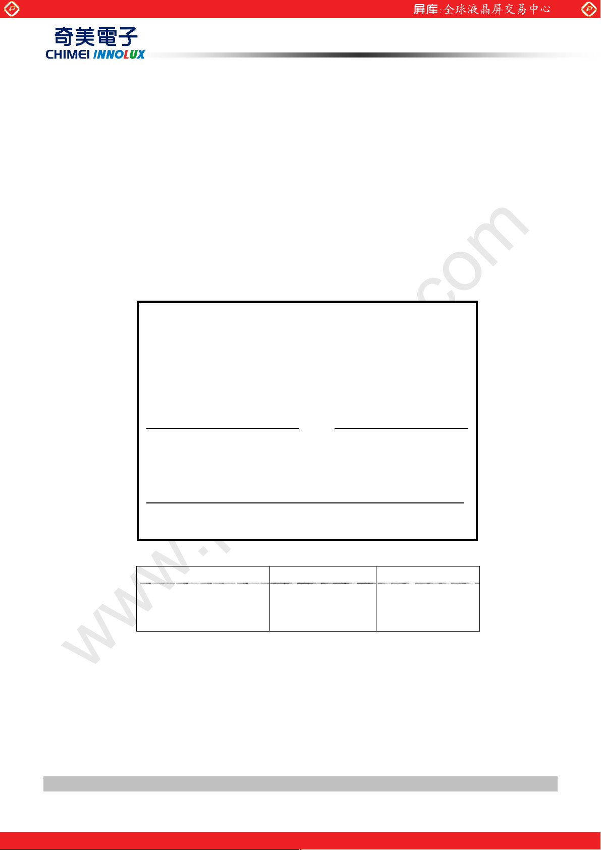
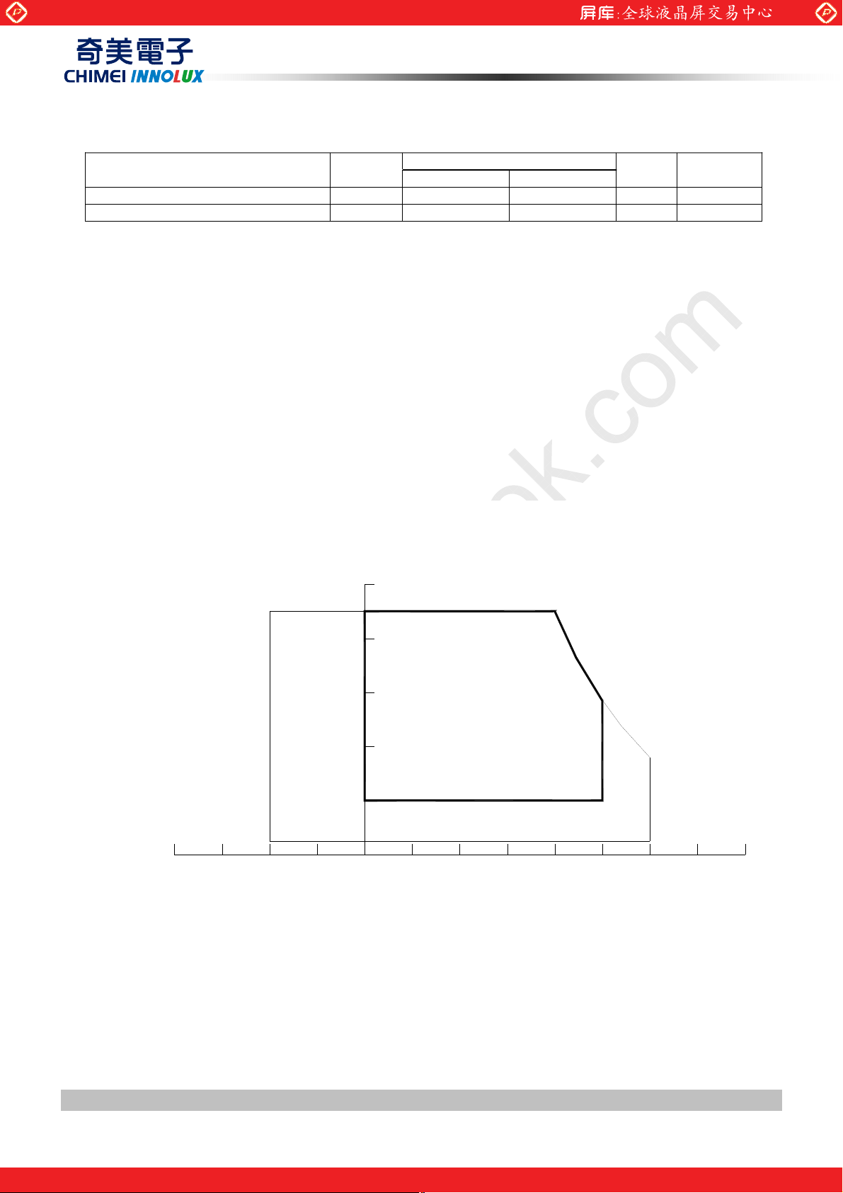
1.3 MECHANICAL SPECIFICATIONS
Item Min. Typ. Max. Unit Note
Weight 905 g -
I/F connector mounting position
Note (1) Please refer to the attached drawings for more information of front and back outline dimensions.
Note (2) Connector mounting position
The mounting inclination of the connector makes the
screen center within ± 0.5mm as the horizontal.
(2)
Version 2.0 4 DateΚΚΚΚ2 Mar. 2012
The copyright belongs to CHIMEI InnoLux. Any unauthorized use is prohibited
One step solution for LCD / PDP / OLED panel application: Datasheet, inventory and accessory!
www.panelook.com
Page 5
Global LCD Panel Exchange Center
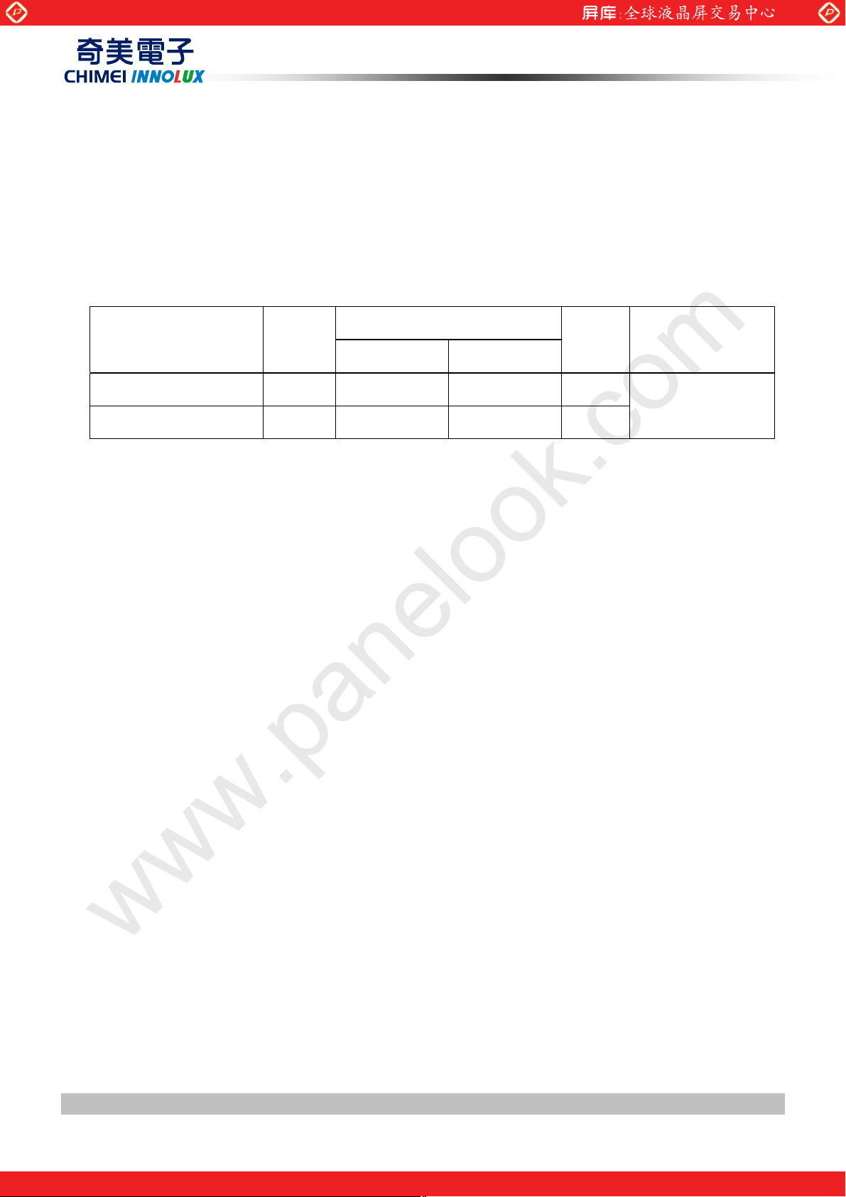
2. ABSOLUTE MAXIMUM RATINGS
2.1 ABSOLUTE RATINGS OF ENVIRONMENT
Item Symbol
Storage Temperature TST -20 +60 ºC (1)
Operating Ambient Temperature T
Note (1) Temperature and relative humidity range is shown in the figure below.
(a) 90 %RH Max. (Ta 40 ºC).Љ
(b) Wet-bulb temperature should be 39 ºC Max. (Ta > 40 ºC).
(c) No condensation.
Note (2) The maximum operating temperature is based on the test condition that the surface temperature of
display area is less than or equal to 65 ºC with LCD module alone in a temperature controlled chamber.
Thermal management should be considered in final product design to prevent the surface temperature
of display area from being over 65 ºC. The range of operating temperature may degrade in case of
www.panelook.com
PRODUCT SPECIFICATION
OP
Value
Min. Max.
0 50 ºC (1), (2)
Unit Note
improper thermal management in final product design.
Relative Humidity (%RH)
100
90
80
60
Operating Range
40
20
10
Storage Range
Temperature (ºC)
Version 2.0 5 DateΚΚΚΚ2 Mar. 2012
The copyright belongs to CHIMEI InnoLux. Any unauthorized use is prohibited
One step solution for LCD / PDP / OLED panel application: Datasheet, inventory and accessory!
8060-20 40020-40
www.panelook.com
Page 6
Global LCD Panel Exchange Center
2.2 PACKAGE STORAGE
When storing modules as spares for a long time, the following precaution is necessary.
(a) Do not leave the module in high temperature, and high humidity for a long time. It is highly recommended to
store the module with temperature from 0 to 35 at normal humidity without к condensation.
(b) The module shall be stored in dark place. Do not store the TFT-LCD module in direct sunlight or fluorescent
light.
2.3 ELECTRICAL ABSOLUTE RATINGS
2.3.1 TFT LCD MODULE
Item Symbol
Power Supply Voltage VCC -0.3 13.5 V
Logic Input Voltage VIN -0.3 3.6 V
www.panelook.com
PRODUCT SPECIFICATION
Value
Unit Note
Min. Max.
(1)
Version 2.0 6 DateΚΚΚΚ2 Mar. 2012
The copyright belongs to CHIMEI InnoLux. Any unauthorized use is prohibited
One step solution for LCD / PDP / OLED panel application: Datasheet, inventory and accessory!
www.panelook.com
Page 7
Global LCD Panel Exchange Center
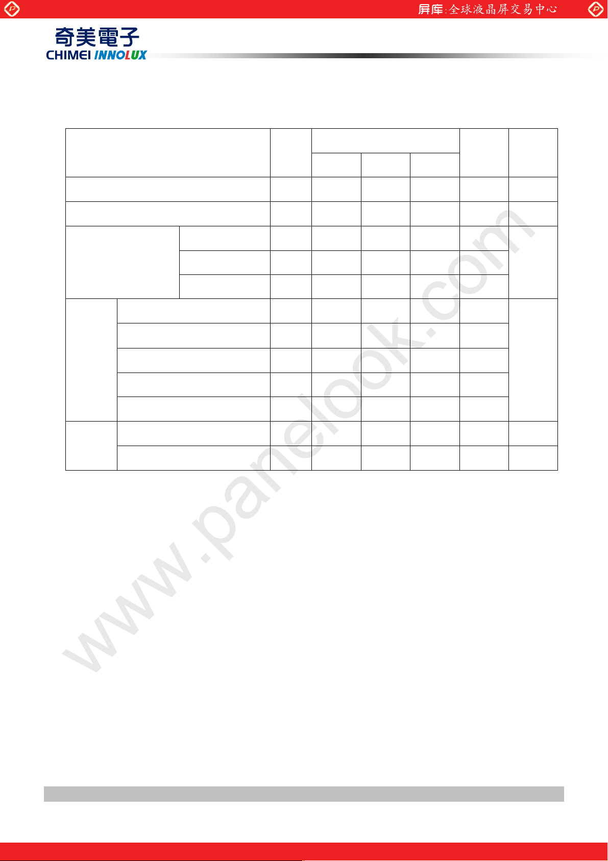
3. ELECTRICAL CHARACTERISTICS
3.1 TFT LCD MODULE
(Ta = 25 ± 2 ºC)
Parameter Symbol
Power Supply Voltage VCC 10.8 12 13.2 V (1)
www.panelook.com
PRODUCT SPECIFICATION
Value
Unit Note
Min. Typ. Max.
Rush Current I
White Pattern
Power Supply Current
Horizontal Stripe
Black Pattern
Differential Input High
Threshold Voltage
Differential Input Low
Threshold Voltage
LVDS
interface
Common Input Voltage VCM 1.0 1.2 1.4 V
Differential input voltage |VID| 200
Terminating Resistor R
CMOS
interface
Input High Threshold Voltage VIH 2.7
Input Low Threshold Voltage V
RUSH
ЁЁ
ЁЁ
ЁЁ
V
LVT H
V
LVT L
T
0
IL
ЁЁ
0.29 0.35 A
0.46 0.56 A
0.26 0.31 A
+100
ЁЁ
ЁЁ
Ё
Ё
100
Ё
Ё
Note (1) The module should be always operated within the above ranges.
3 A (2)
(3)
mV
-100 mV
(4)
600 MV
Ё
Ohm
3.3 V
0.7 V
Note (2) Measurement condition:
Version 2.0 7 DateΚΚΚΚ2 Mar. 2012
The copyright belongs to CHIMEI InnoLux. Any unauthorized use is prohibited
One step solution for LCD / PDP / OLED panel application: Datasheet, inventory and accessory!
www.panelook.com
Page 8
Global LCD Panel Exchange Center
www.panelook.com
PRODUCT SPECIFICATION
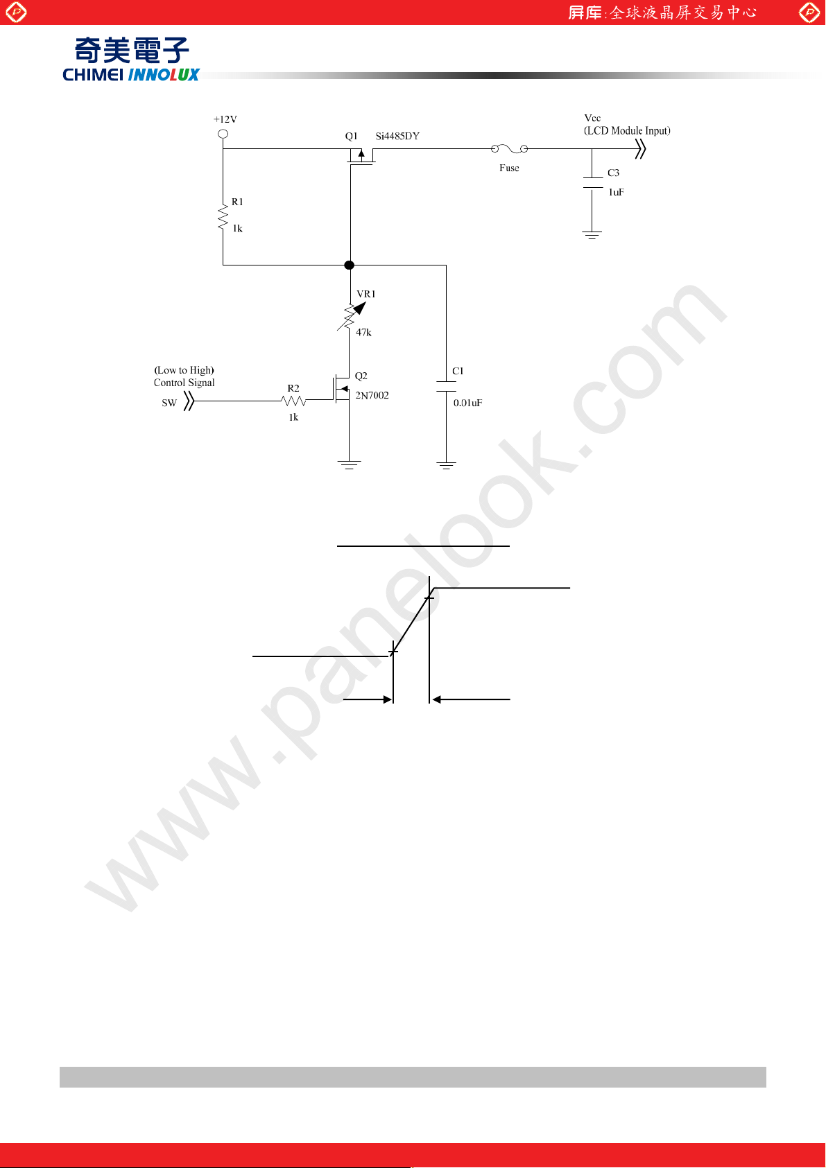
Vcc rising time is 470us
Vcc
0.9Vcc
0.1Vcc
GND
470us
Note (3) The specified power supply current is under the conditions at Vcc = 12 V, Ta = 25 ± 2 ºC, fv = 120 Hz,
whereas a power dissipation check pattern below is displayed.
Version 2.0 8 DateΚΚΚΚ2 Mar. 2012
The copyright belongs to CHIMEI InnoLux. Any unauthorized use is prohibited
One step solution for LCD / PDP / OLED panel application: Datasheet, inventory and accessory!
www.panelook.com
Page 9
Global LCD Panel Exchange Center
www.panelook.com
PRODUCT SPECIFICATION
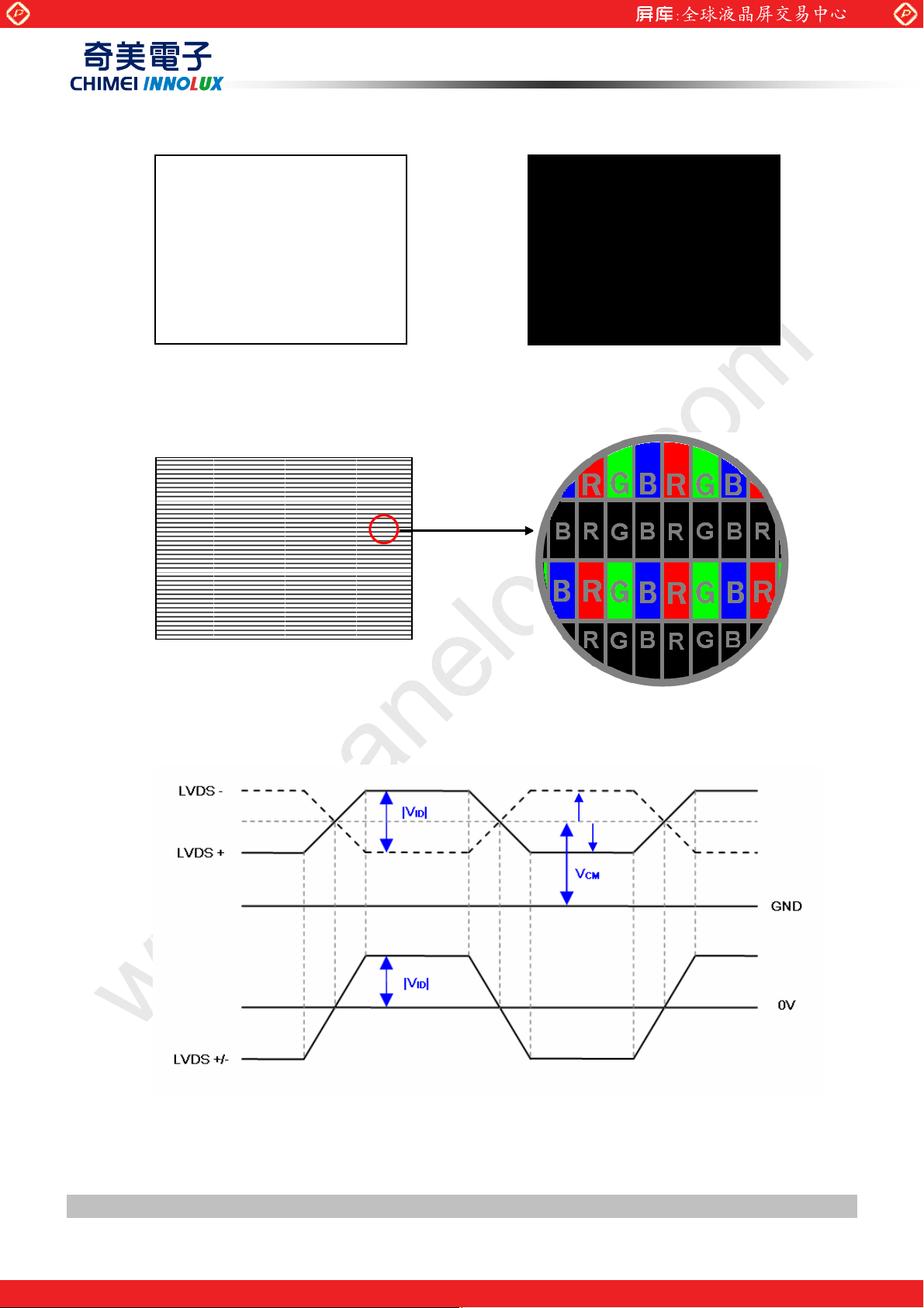
a. White Pattern
Active Area
c. Horizontal Pattern
b. Black Pattern
Active Area
Note (4) The LVDS input characteristics are as follows:
VLVT H
VLVT L
Version 2.0 9 DateΚΚΚΚ2 Mar. 2012
The copyright belongs to CHIMEI InnoLux. Any unauthorized use is prohibited
One step solution for LCD / PDP / OLED panel application: Datasheet, inventory and accessory!
www.panelook.com
Page 10
Global LCD Panel Exchange Center
q
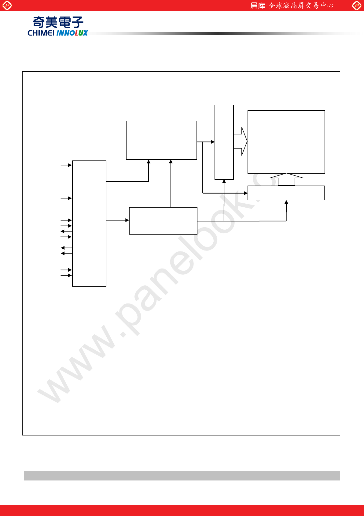
4. BLOCK DIAGRAM OF INTERFACE
4.1 TFT LCD MODULE
www.panelook.com
PRODUCT SPECIFICATION
SCAN DRIVER
ERX0(+/-)
ERX1(+/-)
ERX2(+/-)
ERX3(+/-)
ECLK(+/-)
ORX0(+/-)
ORX1(+/-)
ORX2(+/-)
ORX3(+/-)
OCLK(+/-)
SELLVDS
2D/3D
L/R_O
L/R
PWM0
PWM2
VCC
GND
INPUT CONNECTOR
CNF1:
or e
WF23-400-513C FCN
uivalent
TIMING
CONTROLLER
DC/DC CONVERTER
& REFERENCE
VOLTAGE
TFT LCD PANEL
(1366x3x768)
DATA DRIVER
Version 2.0 10 DateΚΚΚΚ2 Mar. 2012
The copyright belongs to CHIMEI InnoLux. Any unauthorized use is prohibited
One step solution for LCD / PDP / OLED panel application: Datasheet, inventory and accessory!
www.panelook.com
Page 11
Global LCD Panel Exchange Center
5. INPUT TERMINAL PIN ASSIGNMENT
5.1 TFT LCD MODULE INPUT
CNF1 Connector Pin Assignment: (WF23-400-513C (FCN) or equivalent)
Pin Name Description Note
1 N.C. No Connection (1)
www.panelook.com
PRODUCT SPECIFICATION
2
SCL
3
SDA
4 N.C. No Connection
5 L/R_O Output signal for Left Right Glasses control
6 N.C. No Connection (1)
7 SELLVDS Input signal for LVDS Data Format Selection (2)(5)
8 N.C. No Connection (1)
9 PWM0 Upper side scanning B/L signal in 3D mode (no reverse panel)
10 PWM2 Lower side scanning B/L signal in 3D mode (no reverse panel)
11 GND Ground
12 ORX0- Odd pixel Negative LVDS differential data input. Channel 0
13 ORX0+ Odd pixel Positive LVDS differential data input. Channel 0
14 ORX1- Odd pixel Negative LVDS differential data input. Channel 1
15 ORX1+ Odd pixel Positive LVDS differential data input. Channel 1
˜˅˖ Serial Clock
(˄˃)
˜˅˖ Serial Clock
(1)
(8)
(9)
(7)
16 ORX2- Odd pixel Negative LVDS differential data input. Channel 2
17 ORX2+ Odd pixel Positive LVDS differential data input. Channel 2
18 GND Ground
19 OCLK- Odd pixel Negative LVDS differential clock input
(7)
20 OCLK+ Odd pixel Positive LVDS differential clock input
21 GND Ground
22 ORX3- Odd pixel Negative LVDS differential data input. Channel 3
(7)
23 ORX3+ Odd pixel Positive LVDS differential data input. Channel 3
24 N.C. No Connection
(1)
25 N.C. No Connection
26 2D/3D Input signal for 2D/3D Mode Selection (3)(6)
27 L/R Input signal for Left Right eye frame synchronous (4)(6)
28 ERX0- Even pixel Negative LVDS differential data input. Channel 0
(7)
Version 2.0 11 DateΚΚΚΚ2 Mar. 2012
The copyright belongs to CHIMEI InnoLux. Any unauthorized use is prohibited
One step solution for LCD / PDP / OLED panel application: Datasheet, inventory and accessory!
www.panelook.com
Page 12
Global LCD Panel Exchange Center
29 ERX0+ Even pixel Positive LVDS differential data input. Channel 0
30 ERX1- Even pixel Negative LVDS differential data input. Channel 1
31 ERX1+ Even pixel Positive LVDS differential data input. Channel 1
32 ERX2- Even pixel Negative LVDS differential data input. Channel 2
33 ERX2+ Even pixel Positive LVDS differential data input. Channel 2
34 GND Ground
35 ECLK- Even pixel Negative LVDS differential clock input.
36 ECLK+ Even pixel Positive LVDS differential clock input.
37 GND Ground
38 ERX3- Even pixel Negative LVDS differential data input. Channel 3
39 ERX3+ Even pixel Positive LVDS differential data input. Channel 3
www.panelook.com
PRODUCT SPECIFICATION
(7)
(7)
40 N.C. No Connection
41 N.C. No Connection
42 N.C. No Connection
43 N.C. No Connection
44 GND Ground
45 GND Ground
46 GND Ground
47 N.C. No Connection (1)
48 VCC +12V power supply
49 VCC +12V power supply
50 VCC +12V power supply
51 VCC +12V power supply
Note (1) Reserved for internal use. Please leave it open.
(1)
Note (2) LVDS format selection.
L= Connect to GND, H=Connect to +3.3V or Open
SELLVDS Note
L JEIDA Format
H or Open VESA Format
Note (3) 2D/3D mode selection.
L= Connect to GND or Open, H=Connect to +3.3V
2D/3D Note
L or Open 2D Mode
H 3D Mode
Version 2.0 12 DateΚΚΚΚ2 Mar. 2012
The copyright belongs to CHIMEI InnoLux. Any unauthorized use is prohibited
One step solution for LCD / PDP / OLED panel application: Datasheet, inventory and accessory!
www.panelook.com
Page 13

Global LCD Panel Exchange Center
Note (4) Input signal for Left Right eye frame synchronous
www.panelook.com
PRODUCT SPECIFICATION
V
Note (5) SELLVDS signal pin connected to the LCM side has the following diagram.
=0~0.7 V, VIH=2.7~3.3 V
IL
L/R Note
L
H
R1 in the system side should be less than 1K Ohm. (R1 < 1K Ohm)
Right synchronous signal
Left synchronous signal
Note (6) 2D/3D and L/R signal pin connected to the LCM side has the following diagram.
R1 in the system side should be less than 1K Ohm. (R1 < 1K Ohm)
Note (7) Two pixel data send into the module for every clock cycle. The first pixel of the frame is odd pixel and
the second pixel is even pixel.
Note (8) The definition of L/R_O signal as follows
L= 0V , H= +3.3V
L/R_O Note
L
Version 2.0 13 DateΚΚΚΚ2 Mar. 2012
The copyright belongs to CHIMEI InnoLux. Any unauthorized use is prohibited
Right glass turn on
One step solution for LCD / PDP / OLED panel application: Datasheet, inventory and accessory!
www.panelook.com
Page 14

Global LCD Panel Exchange Center
www.panelook.com
PRODUCT SPECIFICATION
H
Note (9) The definition of PWM 0/2 signal as follows
L= 0VʳʿʳH= +3.3˩
PWM 0/2 Note
L
H
Left glass turn on
Note (10) Please reference Appendix A
LED off
LED on
Version 2.0 14 DateΚΚΚΚ2 Mar. 2012
The copyright belongs to CHIMEI InnoLux. Any unauthorized use is prohibited
One step solution for LCD / PDP / OLED panel application: Datasheet, inventory and accessory!
www.panelook.com
Page 15

Global LCD Panel Exchange Center
p
O
p
5.2 BLOCK DIAGRAM OF INTERFACE
www.panelook.com
PRODUCT SPECIFICATION
!
!
!
ER0-ER7
-
-
OR0-OR7
-
-
Host
Graphics
Controller
ERx0+
-
ERx1+
ERx1-
ERx2+
-
ERx3+
ERx3-
ECLK+
-
ORx0+
-
ORx1+
ORx1-
!
51Ө
51Ө
51Ө
51Ө
51Ө
51Ө
51Ө
100pF
51Ө
100pF
100
100pF
RxOUT
ER0-ER7
F
-
-
OR0-OR7
-
!
!
-
51Ө
100pF
51Ө
Timing
51Ө
100pF
51Ө
51Ө
100
F
Controller
ORx2+
Rx2-
ORx3+
ORx3-
OCLK+
LVDS Transmitter
51Ө
100pF
51Ө
51Ө
100pF
51Ө
51Ө
-
100pF
51Ө
LVDS Receiver
THC63LVDM83A
(LVDF83A)
Version 2.0 15 DateΚΚΚΚ2 Mar. 2012
The copyright belongs to CHIMEI InnoLux. Any unauthorized use is prohibited
One step solution for LCD / PDP / OLED panel application: Datasheet, inventory and accessory!
www.panelook.com
Page 16

Global LCD Panel Exchange Center
ER0~ER7: Even pixel R data
EG0~EG7: Even pixel G data
EB0~EB7: Even pixel B data
OR0~OR7: Odd pixel R data
OG0~OG7: Odd pixel G data
OB0~OB7: Odd pixel B data
DE: Data enable signal
DCLK: Data clock signal
Note (1) The system must have the transmitter to drive the module.
Note (2) LVDS cable impedance shall be 50 ohms per signal line or about 100 ohms per twist-pair line
when it is used differentially.
www.panelook.com
PRODUCT SPECIFICATION
Note (3) Two pixel data send into the module for every clock cycle. The first pixel of the frame is odd
pixel and the second pixel is even pixel.
Version 2.0 16 DateΚΚΚΚ2 Mar. 2012
The copyright belongs to CHIMEI InnoLux. Any unauthorized use is prohibited
One step solution for LCD / PDP / OLED panel application: Datasheet, inventory and accessory!
www.panelook.com
Page 17

Global LCD Panel Exchange Center
5.3 LVDS INTERFACE
JEIDA Format : SELLVDS = L
VESA Format : SELLVDS = H or Open
VESA LVDS format
RXCLK
RXCLK
www.panelook.com
PRODUCT SPECIFICATION
Current F\FOH
Current F\FOH
ORX0
ORX0
ORX1
ORX1
ORX2
ORX2
ORX3
ORX3
ERX0
ERX0
ERX1
ERX1
ERX2
ERX2
ERX3
ERX3
JEDIA LVDS format
R5G0 R4 R3 R2 R1
R5G0 R4 R3 R2 R1
B0 G5B1
B0 G5B1
R5G0 R4 R3 R2 R1
R5G0 R4 R3 R2 R1
B0 G5B1
B0 G5B1
Current F\FOH
Current F\FOH
G3 G2G4
G3 G2G4
G3 G2G4
G3 G2G4
R0
R0
G1
G1
B2B4 B3B5VS HSDE
B2B4 B3B5VS HSDE
R6G6 R7G7B7 B6RSVD
R6G6 R7G7B7 B6RSVD
R0
R0
G1
G1
B2B4 B3B5VS HSDE
B2B4 B3B5VS HSDE
R6G6 R7G7B7 B6RSVD
R6G6 R7G7B7 B6RSVD
RXCLK
RXCLK
R7G2 R6 R5 R4 R3
ORX0
ORX0
ORX1
ORX1
ORX2
ORX2
ORX3
ORX3
ERX0
ERX0
ERX1
ERX1
ERX2
ERX2
ERX3
ERX3
Version 2.0 17 DateΚΚΚΚ2 Mar. 2012
The copyright belongs to CHIMEI InnoLux. Any unauthorized use is prohibited
R7G2 R6 R5 R4 R3
B2 G7B3
B2 G7B3
R7G2 R6 R5 R4 R3
R7G2 R6 R5 R4 R3
B2 G7B3
B2 G7B3
G5 G4G6
G5 G4G6
G5 G4G6
G5 G4G6
R2
R2
G3
G3
B4B6 B5B7VS HSDE
B4B6 B5B7VS HSDE
R0G0 R1G1B1 B0RSVD
R0G0 R1G1B1 B0RSVD
R2
R2
G3
G3
B4B6 B5B7VS HSDE
B4B6 B5B7VS HSDE
R0G0 R1G1B1 B0RSVD
R0G0 R1G1B1 B0RSVD
One step solution for LCD / PDP / OLED panel application: Datasheet, inventory and accessory!
www.panelook.com
Page 18

Global LCD Panel Exchange Center
www.panelook.com
PRODUCT SPECIFICATION
R0~R7: Pixel R Data (7; MSB, 0; LSB)
G0~G7: Pixel G Data (7; MSB, 0; LSB)
B0~B7: Pixel B Data (7; MSB, 0; LSB)
DE: Data enable signal
DCLK : Data clock signal
Notes: (1) RSVD (reserved) pins on the transmitter shall be “H” or “L”.
Version 2.0 18 DateΚΚΚΚ2 Mar. 2012
The copyright belongs to CHIMEI InnoLux. Any unauthorized use is prohibited
One step solution for LCD / PDP / OLED panel application: Datasheet, inventory and accessory!
www.panelook.com
Page 19

Global LCD Panel Exchange Center
5.4 COLOR DATA INPUT ASSIGNMENT
The brightness of each primary color (red, green and blue) is based on the 8-bit gray scale data input for the
color. The higher the binary input, the brighter the color. The table below provides the assignment of the color
versus data input.
Color
R7 R6 R5 R4 R3 R2 R1 R0 G7 G6 G5 G4 G3 G2 G1 G0 B7 B6 B5 B4 B3 B2 B1 B0
Black
Red
Green
Basic
Colors
Gray
Scale
Of
Red
Gray
Scale
Of
Green
Gray
Scale
Of
Blue
Note (1) 0: Low Level Voltage, 1: High Level Voltage
Blue
Cyan
Magenta
Yellow
White
Red (0) / Dark
Red (1)
Red (2)
:
:
Red (253)
Red (254)
Red (255)
Green(0) / Dark
Green (1)
Green (2)
:
:
Green (253)
Green (254)
Green (255)
Blue(0) / Dark
Blue (1)
Blue (2)
:
:
Blue (253)
Blue (254)
Blue (255)
0
0
1
1
0
0
0
0
0
0
1
1
1
1
1
1
0
0
0
0
0
0
:
:
:
:
1
1
1
1
1
1
0
0
0
0
0
0
:
:
:
:
0
0
0
0
0
0
0
0
0
0
0
0
:
:
:
:
0
0
0
0
0
0
www.panelook.com
PRODUCT SPECIFICATION
Data Signal
Red Green Blue
0
0
0
0
0
0
0
0
0
0
0
0
0
0
0
1
1
1
1
1
1
0
0
0
0
0
0
0
0
0
0
0
0
0
0
1
1
1
1
1
1
1
1
0
0
0
0
0
0
0
0
0
0
0
0
0
0
0
0
0
0
1
1
1
1
1
1
1
1
1
1
1
1
0
0
0
0
0
0
1
1
1
1
1
1
1
1
1
1
1
1
1
1
1
1
1
1
1
1
1
1
1
1
0
0
0
0
0
0
0
0
0
0
0
0
0
0
0
0
0
1
0
0
0
0
0
0
0
0
1
0
0
0
0
0
:
:
:
:
:
:
:
:
:
:
:
:
:
:
:
:
:
:
:
:
1
1
1
1
0
1
0
0
0
0
1
1
1
1
1
0
0
0
0
0
1
1
1
1
1
1
0
0
0
0
0
0
0
0
0
0
0
0
0
0
0
0
0
0
0
0
0
0
0
0
0
0
0
0
0
0
0
0
0
0
:
:
:
:
:
:
:
:
:
:
:
:
:
:
:
:
:
:
:
:
0
0
0
0
0
0
1
1
1
1
0
0
0
0
0
0
1
1
1
1
0
0
0
0
0
0
1
1
1
1
0
0
0
0
0
0
0
0
0
0
0
0
0
0
0
0
0
0
0
0
0
0
0
0
0
0
0
0
0
0
:
:
:
:
:
:
:
:
:
:
:
:
:
:
:
:
:
:
:
:
0
0
0
0
0
0
0
0
0
0
0
0
0
0
0
0
0
0
0
0
0
0
0
0
0
0
0
0
0
0
0
0
0
0
:
:
:
:
0
0
0
0
0
0
0
0
0
0
0
0
:
:
:
:
1
1
1
1
1
1
0
0
0
0
0
0
:
:
:
:
0
0
0
0
0
0
0
0
1
1
0
0
1
1
1
1
0
0
0
0
0
0
:
:
0
0
0
0
0
0
0
0
0
1
1
0
:
:
0
1
1
0
1
1
0
0
0
0
0
0
:
:
0
0
0
0
0
0
0
0
0
0
0
1
1
1
1
1
1
0
0
1
1
0
0
0
0
0
0
:
:
:
:
:
:
0
0
0
0
0
0
0
0
0
0
0
0
:
:
:
:
:
:
0
0
0
0
0
0
0
0
0
0
0
0
:
:
:
:
:
:
1
1
1
1
1
1
0
0
0
0
0
0
0
0
0
0
0
0
0
0
0
0
0
0
1
1
1
1
1
1
1
1
1
1
1
1
1
1
1
1
1
1
0
0
0
0
0
0
1
1
1
1
1
1
0
0
0
0
0
0
0
0
0
0
0
0
0
0
0
0
0
0
:
:
:
:
:
:
:
:
:
:
:
:
0
0
0
0
0
0
0
0
0
0
0
0
0
0
0
0
0
0
0
0
0
0
0
0
0
0
0
0
0
0
0
0
0
0
0
0
:
:
:
:
:
:
:
:
:
:
:
:
0
0
0
0
0
0
0
0
0
0
0
0
0
0
0
0
0
0
0
0
0
0
0
0
1
0
0
0
0
0
0
1
0
0
0
0
:
:
:
:
:
:
:
:
:
:
:
:
1
0
1
1
1
1
0
1
1
1
1
1
1
1
1
1
1
1
Version 2.0 19 DateΚΚΚΚ2 Mar. 2012
The copyright belongs to CHIMEI InnoLux. Any unauthorized use is prohibited
One step solution for LCD / PDP / OLED panel application: Datasheet, inventory and accessory!
www.panelook.com
Page 20

Global LCD Panel Exchange Center
5.5 FLICKER (VCOM) ADJUSTMENT
(1) Adjustment Pattern:
Flick pattern was shown as below. If customer need below pattern, please directly contact with Account FAE.
. Frame N Frame N+1
www.panelook.com
PRODUCT SPECIFICATION
(2) Adjustment method: (Digital V-com)
Programmable memory IC is used for Digital V-com adjustment in this model. CMI provide Auto Vcom tools
to adjust Digital V-com.The detail connection and setting instruction, please directly contact with Account
FAE to refer CMI Auto V-com adjustment OI.
Version 2.0 20 DateΚΚΚΚ2 Mar. 2012
The copyright belongs to CHIMEI InnoLux. Any unauthorized use is prohibited
One step solution for LCD / PDP / OLED panel application: Datasheet, inventory and accessory!
www.panelook.com
Page 21

Global LCD Panel Exchange Center
6. INTERFACE TIMING
6.1 INPUT SIGNAL TIMING SPECIFICATIONS
(Ta = 25 ± 2 ºC)
The input signal timing specifications are shown as the following table and timing diagram.
Signal Item Symbol Min. Typ. Max. Unit Note
2D mode Frequency
3D mode Frequency
LVDS
Receiver
Clock
Input cycle to
cycle jitter
Spread spectrum
modulation range
Spread spectrum
modulation frequency
www.panelook.com
PRODUCT SPECIFICATION
F
clkin
(=1/TC)
F
clkin
(=1/TC)
- - 200 ps (3)
T
rcl
clkin_mo
F
d
F
- - 200 KHz
SSM
30 38 40 MHz
60 76 80 MHz
F
-2% - F
clkin
+2% MHz
clkin
(4)
LVDS
Receiver
Receiver Skew Margin T
RSKM
-400 - 400 ps (5)
Data
6.1.1 Timing spec for Frame Rate = 50Hz@2D mode, 100Hz@3D mode
Signal Item Symbol Min. Typ. Max. Unit Note
2D mode Fr5 47 50 53 Hz
Frame rate
100 100 100 Hz (7)
r5
ˊˊˉ ˋ˃ˉ ˄˃˄ˋ
ˋˆˋ˅ˈ˃
ˌˉˋ
˅˃˃
Vertical
Active
Display
Te rm
2D Mode
3D Mdoe
3D mode F
Total Tv
Display Tvd 768 768 768 Th
Blank Tvb
Total Tv
Display Tvd 768 Th
Blank Tvb
Th Tv=Tvd+Tvb
Ё
Th
Ё
Th
(6), (8)
Th
Total Th 721 780 1003 Tc Th=Thd+Thb
2D Mode
Horizontal
Active
Display
Te rm
3D Mdoe
Display Thd 683 683 683 Tc
Blank Thb 38 97 320 Tc
Total Th 721 780 1003 Tc Th=Thd+Thb
Display Thd 683 683 683 Tc
Blank Thb 38 97 320 Tc
Version 2.0 21 DateΚΚΚΚ2 Mar. 2012
The copyright belongs to CHIMEI InnoLux. Any unauthorized use is prohibited
One step solution for LCD / PDP / OLED panel application: Datasheet, inventory and accessory!
Ё
Ё
Ё
Ё
www.panelook.com
Page 22

Global LCD Panel Exchange Center
www.panelook.com
PRODUCT SPECIFICATION
6.1.2 Timing spec for Frame Rate = 60Hz@2D mode, 120Hz@3D mode
Signal Item Symbol Min. Typ. Max. Unit Note
2D mode Fr6 57 60 63 Hz
Frame rate
120 120 120 Hz (7)
r6
2D Mode
3D mode F
Total Tv 776 806 1018 Th
Display Tvd 768 768 768 Th
Tv=Tvd+Tv
b
Ё
Vertical
Active
Display
Te rm
3D Mdoe
2D Mode
Horizontal
Active
Display
Te rm
3D Mdoe
Note (1) Since the module is operated in DE only mode, Hsync and Vsync input signals should be set to low
logic level. Otherwise, this module would operate abnormally.
Blank Tvb 8 38 250 Th
Total Tv 806 Th
Display Tvd 768 Th
Blank Tvb 38 Th
Total Th 721 780 1003 Tc
Display Thd 683 683 683 Tc
Blank Thb 38 97 320 Tc
Total Th 721 780 1003 Tc
Display Thd 683 683 683 Tc
Blank Thb 38 97 320 Tc
Ё
(6), (8)
Th=Thd+T
hb
Ё
Ё
Th=Thd+T
hb
Ё
Ё
Note (2) Please make sure the range of pixel clock has follow the below equation:
F
clkin(max)
F
r5
Tv ThѼѼ FЊ
Version 2.0 22 DateΚΚΚΚ2 Mar. 2012
FЊr6 Tv ThѼѼ
clkin(min)
The copyright belongs to CHIMEI InnoLux. Any unauthorized use is prohibited
One step solution for LCD / PDP / OLED panel application: Datasheet, inventory and accessory!
www.panelook.com
Page 23

Global LCD Panel Exchange Center
b
c
www.panelook.com
PRODUCT SPECIFICATION
INPUT SIGNAL TIMING DIAGRAM
Tv
DE
DCLK
DE
DATA
Th
Tvd
T
Th
Thd
Tvb
Valid display data ( 683 clocks)
Note (3) The input clock cycle-to-cycle jitter is defined as below figures. Trcl = I T1 – TI
Version 2.0 23 DateΚΚΚΚ2 Mar. 2012
The copyright belongs to CHIMEI InnoLux. Any unauthorized use is prohibited
One step solution for LCD / PDP / OLED panel application: Datasheet, inventory and accessory!
www.panelook.com
Page 24

Global LCD Panel Exchange Center
www.panelook.com
PRODUCT SPECIFICATION
Note (4) The SSCG (Spread spectrum clock generator) is defined as below figures.
Note (5) The LVDS timing diagram and setup/hold time is defined and showing as the following figures.
LVDS RECEIVER INTERFACE TIMING DIAGRAM
Tc
RXCLK+/-
RXn+/-
T
RSKM
Note (6) Please fix the Vertical timing (Vertical Total =ˌˉˋ / Display =768 / Blank = ˅˃˃) in 100Hz 3D mode
and Vertical timing (Vertical Total =806 / Display =768 / Blank = 38) in 120Hz 3D mode
Note (7) In 3D mode, the set up Fr5 and Fr6 in Typ. ±3 HZ .In order to ensure that the electric function performance
to avoid no display symptom.(Except picture quality symptom.)
Note (8) In 3D mode, the set up Tv and Tvb in Typ. ±30.In order to ensure that the electric function performance to
avoid no display symptom.(Except picture quality symptom.)
Version 2.0 24 DateΚΚΚΚ2 Mar. 2012
The copyright belongs to CHIMEI InnoLux. Any unauthorized use is prohibited
One step solution for LCD / PDP / OLED panel application: Datasheet, inventory and accessory!
www.panelook.com
Page 25

Global LCD Panel Exchange Center
P
6.2 POWER ON/OFF SEQUENCE
(Ta = 25 ± 2 ºC)
6.2.1 POWER ON/OFF SEQUENCE
To prevent a latch-up or DC operation of LCD module, the power on/off sequence should be as the diagram
below.
www.panelook.com
PRODUCT SPECIFICATION
0V
0.5ЉЉЉЉT1ЉЉЉЉ10ms
0ЉЉЉЉT
500ms ЉЉЉЉT
LVDS Signals
2Љ
Љ50ms
ЉЉ
0ЉЉЉЉT
3Љ
Љ50ms
ЉЉ
0ЉЉЉЉT7ЉЉЉЉT2
0ЉЉЉЉT8ЉЉЉЉT3
4
0V
Option Signals
(SELLVDS,2D/3D
L/R )
Backlight (Recommended)
500msЉЉЉЉT
100msЉЉЉЉT6
5
0.1VCC
Power On
T7
T2
50%
0.1Vcc
T3T1
T4
T8
50%
T5
T
6
Power ON/OFF Sequence
Version 2.0 25 DateΚΚΚΚ2 Mar. 2012
The copyright belongs to CHIMEI InnoLux. Any unauthorized use is prohibited
One step solution for LCD / PDP / OLED panel application: Datasheet, inventory and accessory!
www.panelook.com
Page 26

Global LCD Panel Exchange Center
www.panelook.com
PRODUCT SPECIFICATION
6.2.2 2D/3D MODE CHANGE SIGNAL SEQUENCE WITHOUT VCC TURN OFF AND TURN ON
VCC
0V
0.5ЉЉЉЉT1ЉЉЉЉ10ms
2Љ
0ЉЉЉЉT
Љ50ms
ЉЉ
LVDS Signals
0V
0Љ
ЉT7ЉЉЉЉT2
ЉЉ
0ЉЉЉЉT10ЉЉЉЉ10ms
2D/3D
0Љ
ЉT9ЉЉЉЉ10ms
ЉЉ
10ЉЉЉЉT12ЉЉЉЉ20ms
˦˦˦˦calar Black Pattern
Insertion
0.9VCC
0.1VCC
Power On
T7
T1
T2
Black Pattern
T10
T
9
T12
Backlight ON/OFF
500msЉЉЉЉT
500msЉЉЉЉT11
5
T5
T11
Note (1) The supply voltage of the external system for the module input should follow the definition of Vcc.
Note (2) Apply the LED voltage within the LCD operation range. When the backlight turns on before the LCD
operation or the LCD turns off before the backlight turns off, the display may momentarily become
abnormal screen.
Note (3) In case of Vcc is in off level, please keep the level of input signals on the low or high impedance. If
T2<0,that maybe cause electrical overstress failure.
Note (4) T4 should be measured after the module has been fully discharged between power off and on period.
Note (5) Interface signal shall not be kept at high impedance when the power is on.
Version 2.0 26 DateΚΚΚΚ2 Mar. 2012
The copyright belongs to CHIMEI InnoLux. Any unauthorized use is prohibited
One step solution for LCD / PDP / OLED panel application: Datasheet, inventory and accessory!
www.panelook.com
Page 27

Global LCD Panel Exchange Center
7. OPTICAL CHARACTERISTICS
7.1 TEST CONDITIONS
Item Symbol Value Unit
www.panelook.com
PRODUCT SPECIFICATION
Ambient Temperature Ta
Ambient Humidity Ha
Supply Voltage VCC 12 V
Input Signal According to typical value in "3. ELECTRICAL CHARACTERISTICS"
Lamp Current IL 16.5 mA
Oscillating Frequency (Inverter) FW 40 KHz
Vertical Frame Rate Fr 60(2D) Hz
The LCD module should be stabilized at given temperature for 1 hour to avoid abrupt temperature change during
measuring in a windless room.
25±2
50±10
o
C
%RH
Version 2.0 27 DateΚΚΚΚ2 Mar. 2012
The copyright belongs to CHIMEI InnoLux. Any unauthorized use is prohibited
One step solution for LCD / PDP / OLED panel application: Datasheet, inventory and accessory!
www.panelook.com
Page 28

Global LCD Panel Exchange Center
7.2 OPTICAL SPECIFICATIONS
The relative measurement methods of optical characteristics are shown as below. The following items
should be measured under the test conditions described in 7.1 and stable environment shown in 7.1.
Item Symbol Condition Min. Typ. Max. Unit Note
www.panelook.com
PRODUCT SPECIFICATION
Color
Chromaticity
Red
Green
Blue
Rcx
Rcy
Gcx
Gcy
Bcx
Bcy
Wcx
θ
=0°, θY =0°
x
Viewing Angle at Normal
Direction
Standard light source “C”
Typ.
-0.03
0.654
0.328
0.275
0.591
0.131
0.123
0.302
Typ.
+0.03
-
-
-
(0)
-
-
-
White
Wcy
Center Transmittance T% - 5.4 - % (1),(6)
Contrast Ratio CR
Response Time
White Variation
Gray to
gray
δW
θx+
=0°, θY =0°
θ
x
with CMI module
=0°, θY =0°
θ
x
with CMI Module
θ
=0°, θY =0°
x
with CMI module
2100 3000
- 8.5 16 ms (1),(4)
- - 1.4 - (1),(5)
80
0.354
88
- - (1),(3)
-
-
Horizontal
Viewing
Angle
θ
x
θY+
-
80
With CMI module
80
88
88
Deg. (1),(2)
-
Vertical
θ
-
Y
80
88
-
Note (0) Light source is the standard light source ”C” which is defined by CIE and driving voltage are based on
suitable gamma voltages. The calculating method is as following:
1. Measure Module’s and BLU’s spectrum at center point. White is without signal input and R,G,B are
with signal input. BLU (for V320BK1-LD1) is supplied by CMI.
2. Calculate cell’s spectrum.
3. Calculate cell’s chromaticity by using the spectrum of standard light source “C”.
Note (1) Light source is the BLU which supplied by CMI and driving voltage are based on suitable gamma
voltages.
Version 2.0 28 DateΚΚΚΚ02 Mar. 2012
The copyright belongs to CHIMEI InnoLux. Any unauthorized use is prohibited
One step solution for LCD / PDP / OLED panel application: Datasheet, inventory and accessory!
www.panelook.com
Page 29

Global LCD Panel Exchange Center
Note (2) Definition of Viewing Angle (θx, θy):
Viewing angles are measured by Autronic Conoscope Cono-80
www.panelook.com
PRODUCT SPECIFICATION
Normal
θx = θy = 0º
θy- θy+
θX- = 90º
6 o’clock
θ
y-
= 90º
x-
y-
Note (3) Definition of Contrast Ratio (CR):
The contrast ratio can be calculated by the following expression.
Contrast Ratio (CR) =
L255: Luminance of gray level 255
L 0: Luminance of gray level 0
CR = CR (5), where CR (X) is corresponding to the Contrast Ratio of the point X at the figure in Note (5).
θx−
θx+
12 o’clock direction
y+
θ
y+
= 90º
x+
θX+ = 90º
L255 of Luminance Surface
L0 of Luminance Surface
Note (4) Definition of Response Time (T
100%
90%
Optical
Response
10%
0%
, TF):
R
Gray to gray
switching time
Gray to gray
Time
switching time
The driving signal means the signal of gray level 0, 124, 252, 380, 508, 636, 764, 892 and 1023.
Gray to gray average time means the average switching time of gray level 0, 124, 252, 380, 508, 636,
764, 892 and 1023 to each other.
Version 2.0 29 DateΚΚΚΚ02 Mar. 2012
The copyright belongs to CHIMEI InnoLux. Any unauthorized use is prohibited
One step solution for LCD / PDP / OLED panel application: Datasheet, inventory and accessory!
www.panelook.com
Page 30

Global LCD Panel Exchange Center
Note (5) Definition of White Variation (δW):
Measure the luminance of gray level 255 at 5 points
δW = Maximum [L (1), L (2), L (3), L (4), L (5)] / Minimum [L (1), L (2), L (3), L (4), L (5)]
www.panelook.com
PRODUCT SPECIFICATION
Horizontal Line
D
D/4 D/2 3D/4
1 2
W
W/4
W/2
Vertical Line
3W/4
3 4
Note (6) Definition of Transmittance (T%) :
Measure the luminance of gray level 255 at center point of LCD module.
Transmittance (T%) =
5
Active Area
X
: Test Point
X=1 to 5
module LCD of Luminance
100%
unit backligh of Luminance
×
Version 2.0 30 DateΚΚΚΚ02 Mar. 2012
The copyright belongs to CHIMEI InnoLux. Any unauthorized use is prohibited
One step solution for LCD / PDP / OLED panel application: Datasheet, inventory and accessory!
www.panelook.com
Page 31

Global LCD Panel Exchange Center
V
320
8. DEFINITION OF LABELS
8.1 OPEN CELL LABEL
The barcode nameplate is pasted on each open cell as illustration for CMI internal control.
www.panelook.com
PRODUCT SPECIFICATION
V320BK1-PD1
XXXXXXXXXXXXXX
8.2 CARTON LABEL
The barcode nameplate is pasted on each box as illustration, and its definitions are as following explanation
P.O. NO. Made in Taiwan
Part ID. Quantities 10
Model Name.
Carton ID. XXXXXXXXXXXXXX RoHS
XXXXXXXXXXXXXX
BK1-PD1 Rev.
P.O. NO. Made in China
Part ID. Quantities 10
Model Name.
Carton ID. XXXXXXXXXXXXXX RoHS
(a) Model Name: V320BK1– PD1
(b) Carton ID: CMI internal control
(c) Quantities: 10
Version 2.0 31 DateΚΚΚΚ02 Mar. 2012
The copyright belongs to CHIMEI InnoLux. Any unauthorized use is prohibited
One step solution for LCD / PDP / OLED panel application: Datasheet, inventory and accessory!
www.panelook.com
Page 32

Global LCD Panel Exchange Center
9. PACKAGING
9.1 PACKING SPECIFICATIONS
(1) 10 LCD TV Panels / 1 Box
(2) Box dimensions : 810 (L) X 555 (W) X92 (H)mm
(3) Weight :approximately 16Kg ( 10 panels per box)
(4) 260 LCD TV Panels / 1 Group
9.2 PACKING METHOD
Figures 9-1 and 9-2 are the packing method
www.panelook.com
PRODUCT SPECIFICATION
Version 2.0 32 DateΚΚΚΚ02 Mar. 2012
The copyright belongs to CHIMEI InnoLux. Any unauthorized use is prohibited
One step solution for LCD / PDP / OLED panel application: Datasheet, inventory and accessory!
www.panelook.com
Page 33

Global LCD Panel Exchange Center
www.panelook.com
PRODUCT SPECIFICATION
Version 2.0 33 DateΚΚΚΚ02 Mar. 2012
The copyright belongs to CHIMEI InnoLux. Any unauthorized use is prohibited
One step solution for LCD / PDP / OLED panel application: Datasheet, inventory and accessory!
www.panelook.com
Page 34

Global LCD Panel Exchange Center
www.panelook.com
PRODUCT SPECIFICATION
10. PRECAUTIONS
10.1 ASSEMBLY AND HANDLING PRECAUTIONS
(1) Do not apply rough force such as bending or twisting to the product during assembly.
(2) To assemble backlight or install module into user’s system can be only in clean working areas. The dust
and oil may cause electrical short or worsen the polarizer.
(3) It’s not permitted to have pressure or impulse on the module because the LCD panel will be damaged.
(4) Always follow the correct power sequence when the product is connecting and operating. This can
prevent damage to the CMOS LSI chips during latch-up.
(5) Do not pull the I/F connector in or out while the module is operating.
(6) Use a soft dry cloth without chemicals for cleaning, because the surface of polarizer is very soft and
easily scratched.
(7) It is dangerous that moisture come into or contacted the product, because moisture may damage the
product when it is operating.
(8) High temperature or humidity may reduce the performance of module. Please store this product within
the specified storage conditions.
(9) When ambient temperature is lower than 10ºC may reduce the display quality. For example, the
response time will become slowly.
10.2 SAFETY PRECAUTIONS
(1) If the liquid crystal material leaks from the panel, it should be kept away from the eyes or mouth. In case of
contact with hands, skin or clothes, it has to be washed away thoroughly with soap.
(2) After the product’s end of life, it is not harmful in case of normal operation and storage.
Version 2.0 34 DateΚΚΚΚ02 Mar. 2012
The copyright belongs to CHIMEI InnoLux. Any unauthorized use is prohibited
One step solution for LCD / PDP / OLED panel application: Datasheet, inventory and accessory!
www.panelook.com
Page 35

Global LCD Panel Exchange Center
11. MECHANICAL CHARACTERISTIC
www.panelook.com
PRODUCT SPECIFICATION
Version 2.0 35 DateΚΚΚΚ02 Mar. 2012
The copyright belongs to CHIMEI InnoLux. Any unauthorized use is prohibited
One step solution for LCD / PDP / OLED panel application: Datasheet, inventory and accessory!
www.panelook.com
Page 36

Global LCD Panel Exchange Center
www.panelook.com
PRODUCT SPECIFICATION
Version 2.0 36 DateΚΚΚΚ02 Mar. 2012
The copyright belongs to CHIMEI InnoLux. Any unauthorized use is prohibited
One step solution for LCD / PDP / OLED panel application: Datasheet, inventory and accessory!
www.panelook.com
Page 37

Global LCD Panel Exchange Center
Appendix A.
A.1 I2C timing
Symbol Parameter Min. Max. Unit
t
Start setup time 250 - ns
SU-STA
t
Start hold time 250 - ns
HD-STA
t
Data setup time 80 - ns
SU-DAT
t
Data hold time 0 - ns
HD-DAT
t
Stop setup time 250 - ns
SU-STO
www.panelook.com
PRODUCT SPECIFICATION
t
BUF
Time between Stop condition and next
Start condition
500 - ns
Version 2.0 37 DateΚΚΚΚ02 Mar. 2012
The copyright belongs to CHIMEI InnoLux. Any unauthorized use is prohibited
One step solution for LCD / PDP / OLED panel application: Datasheet, inventory and accessory!
www.panelook.com
 Loading...