

Page 1
Global LCD Panel Exchange Center
MODEL NO.: V315H4
www.panelook.com
PRODUCT SPECIFICATION
□ Tentative Specification
□Preliminary Specification
■ Approval Specification
SUFFIX: LE3
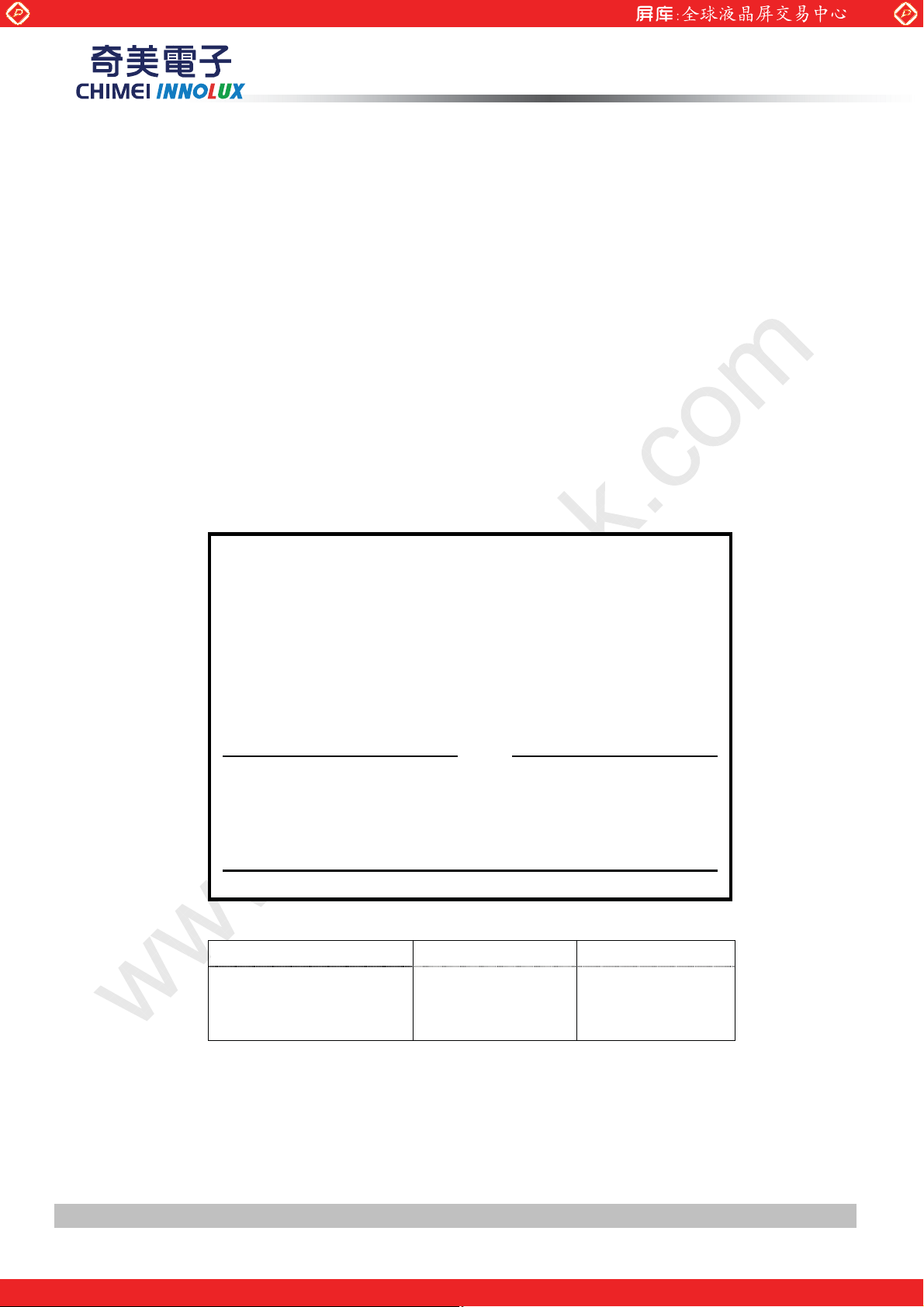
Customer:
APPROVED BY SIGNATURE
Name / Title
Note
Approved By Checked By Prepared By
Chao-Chun Chung Ken Wu Carlos Lee
Version 2.1 1 DateΚΚΚΚ26 Apr 2011
The copyright belongs to CHIMEI InnoLux. Any unauthorized use is prohibited
One step solution for LCD / PDP / OLED panel application: Datasheet, inventory and accessory!
www.panelook.com
Page 2

Global LCD Panel Exchange Center
www.panelook.com
PRODUCT SPECIFICATION
CONTENTS
1. GENERAL DESCRIPTION ......................................................................................................................................................... 5
1.1 OVERVIEW ..........................................................................................................................................................5
1.2 FEATURES ..........................................................................................................................................................5
1.3 APPLICATION...................................................................................................................................................... 5
1.4 GENERAL SPECIFICATIONS .............................................................................................................................5
1.5 MECHANICAL SPECIFICATIONS....................................................................................................................... 5
2. ABSOLUTE MAXIMUM RATINGS .......................................................................................................................................... 6
2.1 ABSOLUTE RATINGS OF ENVIRONMENT ........................................................................................................ 6
2.2 PACKAGE STORAGE.......................................................................................................................................... 7
2.3 ELECTRICAL ABSOLUTE RATINGS .................................................................................................................. 7
3. ELECTRICAL CHARACTERISTICS ......................................................................................................................................... 8
3.1 TFT LCD MODULE ..............................................................................................................................................8
3.2 BACKLIGHT CONNECTOR PIN CONFIGURATION......................................................................................... 11
4. BLOCK DIAGRAM OF INTERFACE ...................................................................................................................................... 12
4.1 TFT LCD MODULE ............................................................................................................................................12
5. INPUT TERMINAL PIN ASSIGNMENT ................................................................................................................................ 13
5.1 TFT LCD Module Input....................................................................................................................................... 13
5.2 BACKLIGHT UNIT.............................................................................................................................................. 15
5.3 BLOCK DIAGRAM OF INTERFACE.................................................................................................................. 16
5.4 LVDS INTERFACE ............................................................................................................................................. 18
5.5 COLOR DATA INPUT ASSIGNMENT ................................................................................................................ 19
6. INTERFACE TIMING................................................................................................................................................................ 20
6.1 INPUT SIGNAL TIMING SPECIFICATIONS...................................................................................................... 20
6.2 POWER ON/OFF SEQUENCE..........................................................................................................................23
7. OPTICAL CHARACTERISTICS............................................................................................................................................... 24
7.1 TEST CONDITIONS...........................................................................................................................................24
7.2 OPTICAL SPECIFICATIONS .............................................................................................................................25
8. PRECAUTIONS .......................................................................................................................................................................... 29
8.1 ASSEMBLY AND HANDLING PRECAUTIONS .................................................................................................29
8.2 SAFETY PRECAUTIONS ..................................................................................................................................29
Version 2.1 2 DateΚΚΚΚ26 Apr 2011
The copyright belongs to CHIMEI InnoLux. Any unauthorized use is prohibited
One step solution for LCD / PDP / OLED panel application: Datasheet, inventory and accessory!
www.panelook.com
Page 3
Global LCD Panel Exchange Center
www.panelook.com
PRODUCT SPECIFICATION
8.3 STORAGE PRECAUTIONS............................................................................................................................... 29
9. DEFINITION OF LABELS......................................................................................................................................................... 30
9.1 CMI MODULE LABEL ........................................................................................................................................30
10. MECHANICAL CHARACTERISTIC .................................................................................................................................... 31
Version 2.1 3 DateΚΚΚΚ26 Apr 2011
The copyright belongs to CHIMEI InnoLux. Any unauthorized use is prohibited
One step solution for LCD / PDP / OLED panel application: Datasheet, inventory and accessory!
www.panelook.com
Page 4
Global LCD Panel Exchange Center
Version Date Page(New) Section Description
Ver. 0. 0
Ver. 1. 0
Ver. 2. 0
Ver. 2. 1
Dec. 08, 2010
Dec.28, 2010
Jan. 14, 2011
Apr. 26, 2011
All
All
All
15
www.panelook.com
PRODUCT SPECIFICATION
REVISION HISTORY
All
All
All
5.2
The tentative specification was first issued.
The preliminary specification was first issued.
The Approval Specification was first issued.
Modify PIN ASSIGNMENT
Version 2.1 4 DateΚΚΚΚ26 Apr 2011
The copyright belongs to CHIMEI InnoLux. Any unauthorized use is prohibited
One step solution for LCD / PDP / OLED panel application: Datasheet, inventory and accessory!
www.panelook.com
Page 5
Global LCD Panel Exchange Center
1. GENERAL DESCRIPTION
1.1 OVERVIEW
V315H4-LE3 is a TFT Liquid Crystal Display module with LED Backlight unit and 2ch-LVDS interface. The display
diagonal is 31.5”. This module supports 1920 x 1080 Full HDTV format and can display 16.7M colors (8-bit). The
converter module for backlight isn’t built-in.
1.2 FEATURES
Ё High contrast ratio (4000:1)
Ё Fast response time (8.5ms)
Ё High color saturation (NTSC 72%)
Ё Full HDTV (1920 x 1080 pixels) resolution, true HDTV format
Ё DE (Data Enable) only mode
www.panelook.com
PRODUCT SPECIFICATION
Ё LVDS (Low Voltage Differential Signaling) interface
Ё Viewing Angle : 176(H)/176(V) (CR>20) MVA Technology
Ё RoHs compliance
1.3 APPLICATION
Ё TFT LCD TVs
Ё Multi-Media Displays
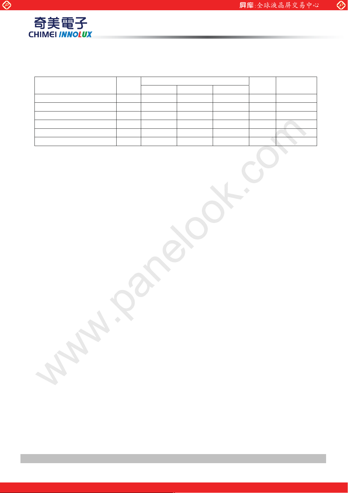
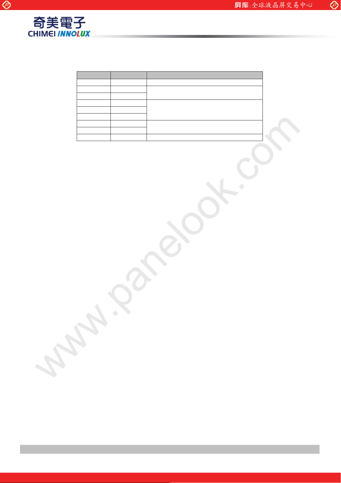
1.4 GENERAL SPECIFICATIONS
Item Specification Unit Note
Active Area 697.92(H) x 392.58 (V) mm (1)
Driver Element a-si TFT active matrix - -
Pixel Number 1920 x W. R.G.B. x 1080 pixel -
Pixel Pitch(Sub Pixel) 0.18175 (H) x 0.18175 (V) mm -
Pixel Arrangement wRGB square - -
Display Colors 16.7M color -
Display Operation Mode Transmissive mode / Normally Black - -
Surface Treatment Anti-Glare coating (Haze 14%) / Hard Coating (3H) - (2)
Note (1) Please refer to the attached drawings for more information about the front and back outlines.
Note (2) The spec. of the surface treatment is temporarily for this phase. CMI reserves the rights to change this feature.
1.5 MECHANICAL SPECIFICATIONS
Item Min. Typ. Max. Unit Note
Horizontal (H) 740.4 741.4 742.4 mm Module size
Module Size
Weight - 3710 - g -
Vertical (V) 435.0 435.8 436.6 mm
Depth (D) 8.9 9.4 9.9 mm To rear
Version 2.1 5 DateΚΚΚΚ26 Apr 2011
The copyright belongs to CHIMEI InnoLux. Any unauthorized use is prohibited
One step solution for LCD / PDP / OLED panel application: Datasheet, inventory and accessory!
www.panelook.com
Page 6
Global LCD Panel Exchange Center
2. ABSOLUTE MAXIMUM RATINGS
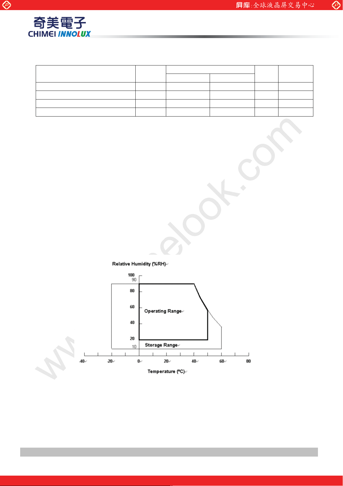
2.1 ABSOLUTE RATINGS OF ENVIRONMENT
Item Symbol
Storage Temperature TST -20 +60 ºC (1)
Operating Ambient Temperature TOP 0 50 ºC (1), (2)
Shock (Non-Operating) SNOP - 50 G (3), (5)
Vibration (Non-Operating) VNOP - 1.0 G (4), (5)
Note (1) Temperature and relative humidity range is shown in the figure below.
(a) 90 %RH Max. (Ta Љ 40 ºC).
(b) Wet-bulb temperature should be 39 ºC Max. (Ta > 40 ºC).
(c) No condensation.
Note (2) The maximum operating temperature is based on the test condition that the surface temperature of
www.panelook.com
PRODUCT SPECIFICATION
Value
Min. Max.
Unit Note
display area is less than or equal to 65 ºC with LCD module alone in a temperature controlled chamber.
Thermal management should be considered in final product design to prevent the surface temperature
of display area from being over 65 ºC. The range of operating temperature may degrade in case of
improper thermal management in final product design.
Note (3) 11 ms, half sine wave, 1 time for ± X, ± Y, ± Z.
Note (4) 10 ~ 200 Hz, 10 min, 1 time each X, Y, Z.
Note (5) At testing Vibration and Shock, the fixture in holding the module has to be hard and rigid enough so that
the module would not be twisted or bent by the fixture.
Version 2.1 6 DateΚΚΚΚ26 Apr 2011
The copyright belongs to CHIMEI InnoLux. Any unauthorized use is prohibited
One step solution for LCD / PDP / OLED panel application: Datasheet, inventory and accessory!
www.panelook.com
Page 7
Global LCD Panel Exchange Center
2.2 PACKAGE STORAGE
When storing modules as spares for a long time, the following precaution is necessary.
(a) Do not leave the module in high temperature, and high humidity for a long time, It is highly recommended to
store the module with temperature from 0 to 35 к at normal humidity without condensation.
(b) The module shall be stored in dark place. Do not store the TFT-LCD module in direct sunlight or fluorescent
light.
2.3 ELECTRICAL ABSOLUTE RATINGS
2.3.1 TFT LCD MODULE
Item Symbol
Power Supply Voltage Vcc -0.3 13.5 V
Input Signal Voltage VIN -0.3 3.6 V
www.panelook.com
PRODUCT SPECIFICATION
Value
Min. Max.
Unit Note
(1)
Version 2.1 7 DateΚΚΚΚ26 Apr 2011
The copyright belongs to CHIMEI InnoLux. Any unauthorized use is prohibited
One step solution for LCD / PDP / OLED panel application: Datasheet, inventory and accessory!
www.panelook.com
Page 8

Global LCD Panel Exchange Center
3. ELECTRICAL CHARACTERISTICS
3.1 TFT LCD MODULE
(Ta = 25 ± 2 ºC)
Parameter Symbol
Power Supply Voltage VCC 10.8 12 13.2 V (1)
www.panelook.com
PRODUCT SPECIFICATION
Value
Unit Note
Min. Typ. Max.
Rush Current I
White Pattern
Power consumption
Horizontal Stripe
Black Pattern
White Pattern
Power Supply Current
Horizontal Stripe
Black Pattern
Differential Input High
Threshold Voltage
Differential Input Low
Threshold Voltage
LVDS
interface
Common Input Voltage VCM 1.0 1.2 1.4 V
Differential input voltage
(single-end)
Terminating Resistor R
RUSH
ЁЁ
Ё
P
T
Ё
Ё
ЁЁ
ЁЁ
ЁЁ
V
V
|V
LVT H
LVT L
ID
T
+100
ЁЁ
| 200
Ё
3.7 A (2)
6.72 8.16 W
7.92 9.84 W
4.8 5.76 W
0.56 0.68 A
0.66 0.82 A
0.4 0.48 A
ЁЁ
mV
-100 mV
Ё
100
600 mV
Ё
ohm
(3)
(4)
(5)
CMIS
interface
Input High Threshold Voltage VIH 2.7
Input Low Threshold Voltage V
0
IL
Ё
Ё
3.3 V
0.7 V
Note (1) The module should be always operated within the above ranges.
Version 2.1 8 DateΚΚΚΚ26 Apr 2011
The copyright belongs to CHIMEI InnoLux. Any unauthorized use is prohibited
One step solution for LCD / PDP / OLED panel application: Datasheet, inventory and accessory!
www.panelook.com
Page 9
Global LCD Panel Exchange Center
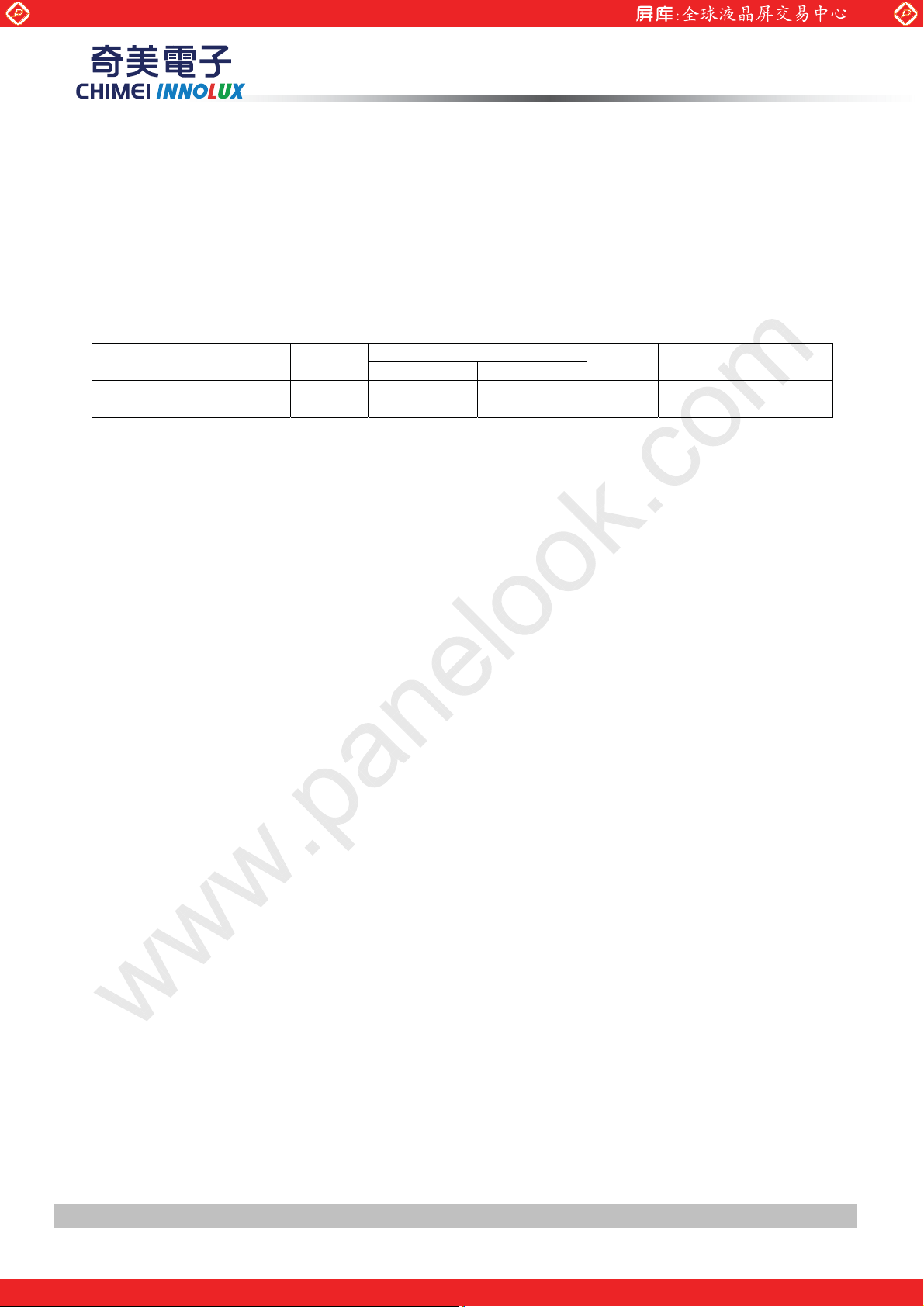
Note (2) Measurement ConditionsΚ
www.panelook.com
PRODUCT SPECIFICATION
GND
Vcc rising time is 470us
Vcc
0.9Vcc
0.1Vcc
470us
Version 2.1 9 DateΚΚΚΚ26 Apr 2011
The copyright belongs to CHIMEI InnoLux. Any unauthorized use is prohibited
One step solution for LCD / PDP / OLED panel application: Datasheet, inventory and accessory!
www.panelook.com
Page 10
Global LCD Panel Exchange Center
www.panelook.com
PRODUCT SPECIFICATION
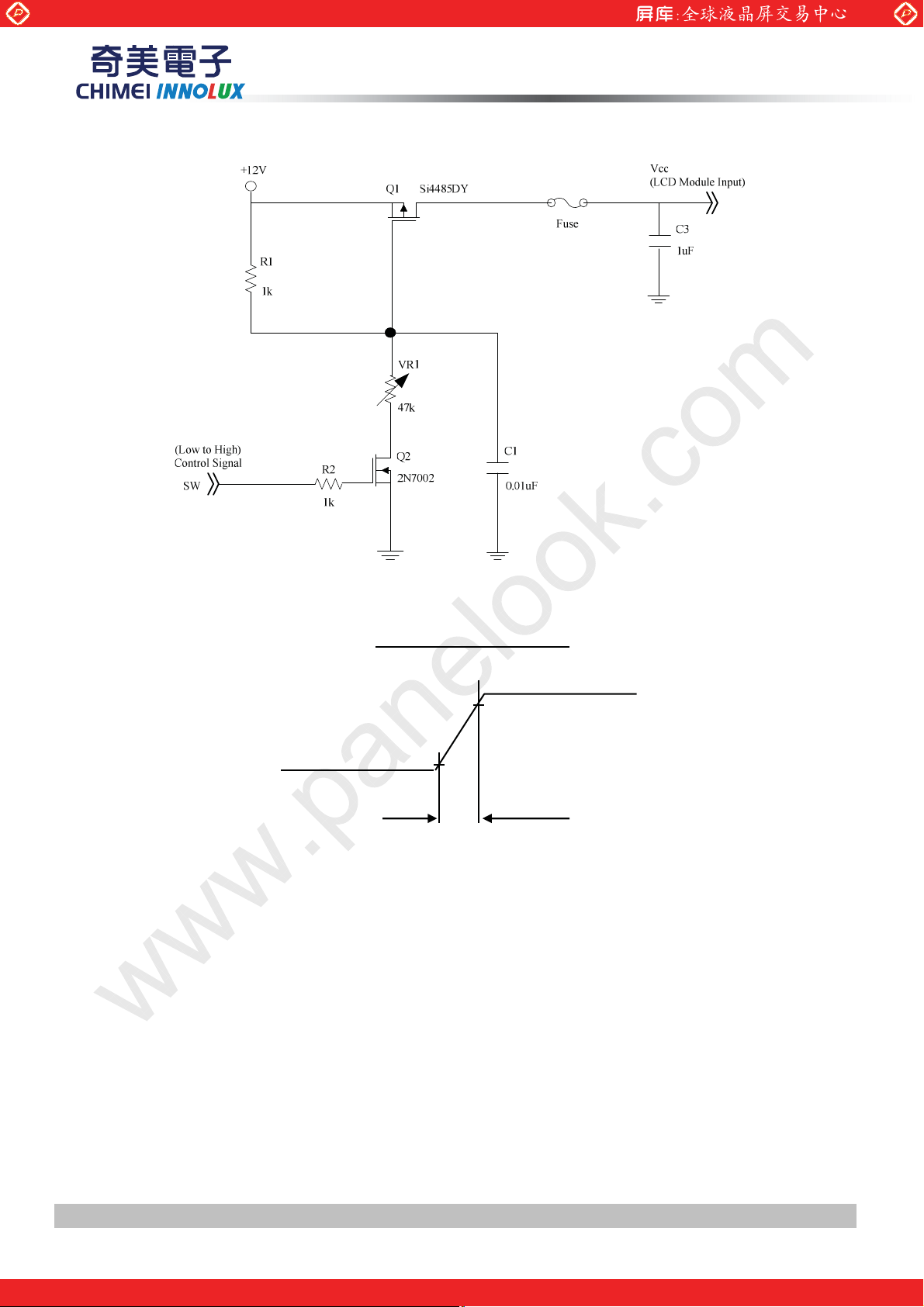
Note (3) The Specified Power consumption is under a,b,c pattern.
Note (4) The Specified power supply current is under the conditions at Vcc = 12 V, Ta = 25 ± 2 ºC, f
whereas a power dissipation check pattern below is displayed.
a. White Pattern
Active Area
c. Horizontal Pattern
b. Black Pattern
Active Area
= 60 Hz,
v
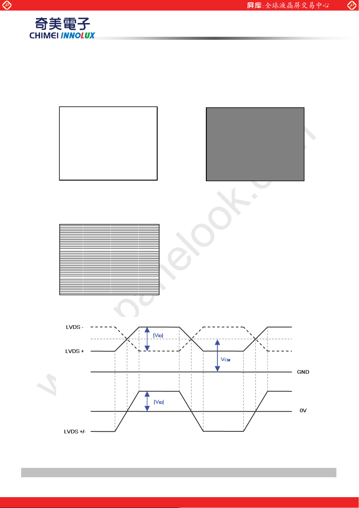
Note (5) The LVDS input characteristics are as follows :
Version 2.1 10 DateΚΚΚΚ26 Apr 2011
The copyright belongs to CHIMEI InnoLux. Any unauthorized use is prohibited
One step solution for LCD / PDP / OLED panel application: Datasheet, inventory and accessory!
www.panelook.com
Page 11
Global LCD Panel Exchange Center
www.panelook.com
3.2 BACKLIGHT CONNECTOR PIN CONFIGURATION
PRODUCT SPECIFICATION
3.2.1 LED LIGHT BAR CHARACTERISTICS (
Ta = 25 ± 2 ºC)
The backlight unit contains 2 pcs light bar.
Parameter Symbol
Total Current (6 String) If
One String Current I
LED Forward Voltage V
One String Voltage V
One String Voltage Variation
ϦV
Life time -
Min. Typ. Max.
- 720 763.2
L
f
W
- - 2
W
- 120 127.2
3.0 3.25 3.5
51 - 59.5
30,000 - -
Value
Unit Note
mA
mA
I
V
DC
I
V
DC
V
Hrs (1)
Note (1) The lifetime is defined as the time which luminance of the LED decays to 50% compared to the
initial value, Operating condition: Continuous operating at Ta = 25±2 , Iк
=120mA.
L
=120mA
L
=120mA
L
Version 2.1 11 DateΚΚΚΚ26 Apr 2011
The copyright belongs to CHIMEI InnoLux. Any unauthorized use is prohibited
One step solution for LCD / PDP / OLED panel application: Datasheet, inventory and accessory!
www.panelook.com
Page 12
Global LCD Panel Exchange Center
)
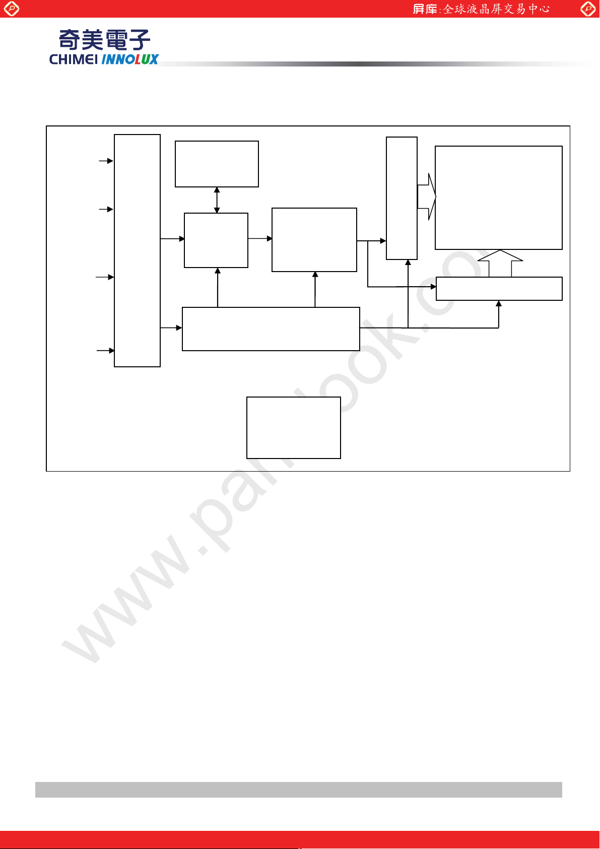
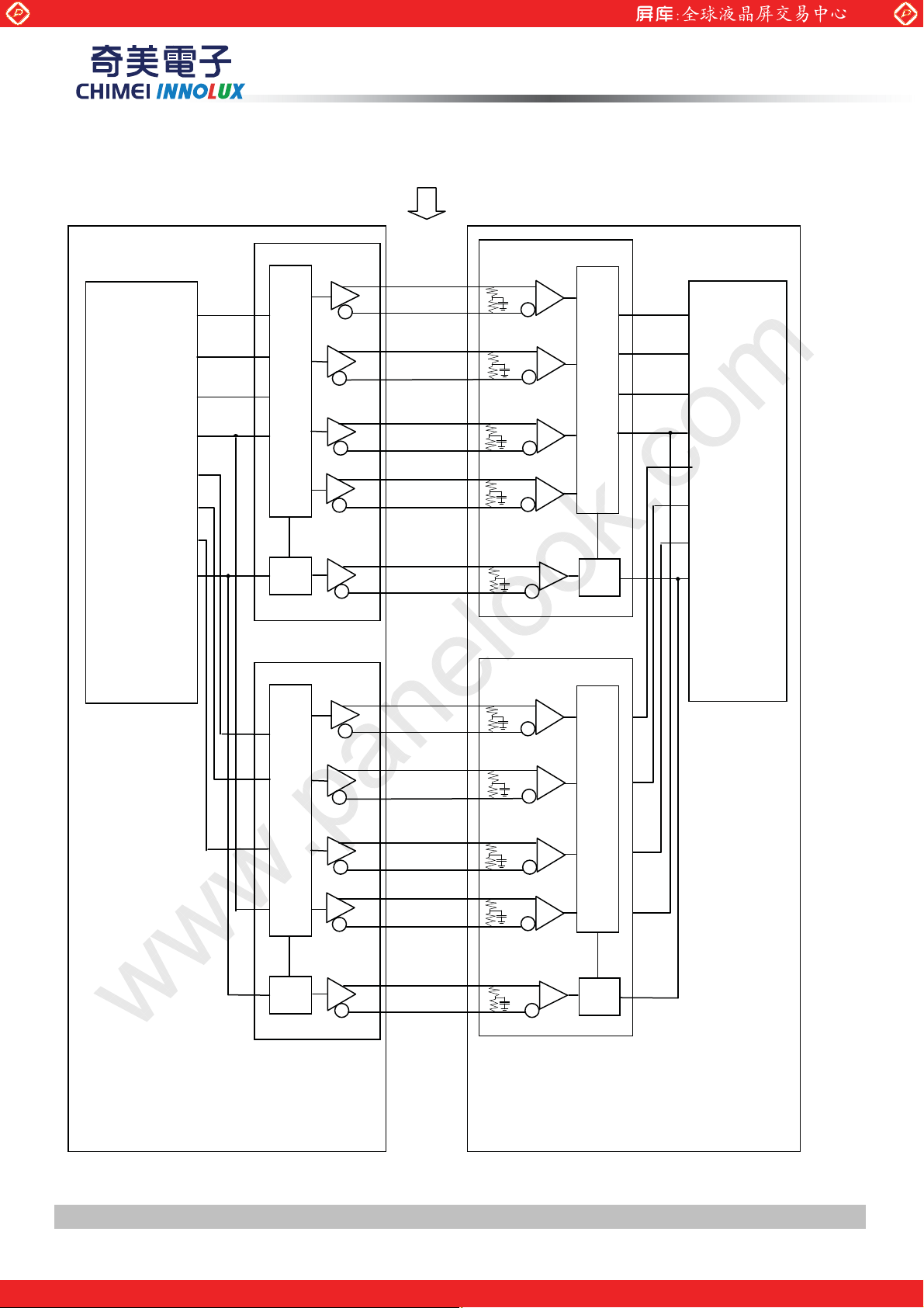
4. BLOCK DIAGRAM OF INTERFACE
4.1 TFT LCD MODULE
ER 0+/ER 1+/ER 2+/ER 3+/ER CLK+/-
OR 0+/OR 1+/OR 2+/OR 3+/OR CLK+/-
(FI-RE51S-HF (JAE)) or equivalent
INPUT CONNECTOR
FRAME
BUFFER
MEMC
SELLVDS
www.panelook.com
PRODUCT SPECIFICATION
SCAN DRIVER
TFT LCD PANEL
(1920x2x1080 x2)
TIMING
CONTROLLER
Data Driver (mini-LVDS
VIN
GND
DC/DC CONVERTER
& REFERENCE VOLTAGE
GENERATOR
CN2:51281-1094 (Molex) or equivalent
LED
BACKLIGHT
UNIT
Version 2.1 12 DateΚΚΚΚ26 Apr 2011
The copyright belongs to CHIMEI InnoLux. Any unauthorized use is prohibited
One step solution for LCD / PDP / OLED panel application: Datasheet, inventory and accessory!
www.panelook.com
Page 13
Global LCD Panel Exchange Center
www.panelook.com
PRODUCT SPECIFICATION
5. INPUT TERMINAL PIN ASSIGNMENT
5.1 TFT LCD Module Input
CNF1 Connector Part No.: JAE Taiwan FI-RE51S-HF or equivalent.
Pin Name Description Note
1 GND Ground
2 N.C. No Connection
3 N.C. No Connection
4 N.C. No Connection
5 N.C. No Connection
6 N.C. No Connection
7 SELLVDS LVDS data format Selection (3) (4)
8 N.C. No Connection
9 N.C. No Connection
10 N.C. No Connection
11 GND Ground
12 ERX0- Even pixel Negative LVDS differential data input. Channel 0
13 ERX0+ Even pixel Positive LVDS differential data input. Channel 0
14 ERX1- Even pixel Negative LVDS differential data input. Channel 1
15 ERX1+ Even pixel Positive LVDS differential data input. Channel 1
16 ERX2- Even pixel Negative LVDS differential data input. Channel 2
17 ERX2+ Even pixel Positive LVDS differential data input. Channel 2
18 GND Ground
19 ECLK- Even pixel Negative LVDS differential clock input.
20 ECLK+ Even pixel Positive LVDS differential clock input.
21 GND Ground
22 ERX3- Even pixel Negative LVDS differential data input. Channel 3
23 ERX3+ Even pixel Positive LVDS differential data input. Channel 3
24 N.C. No Connection
25 N.C. No Connection
26 GND Ground
27 GND Ground
28 ORX0- Odd pixel Negative LVDS differential data input. Channel 0
29 ORX0+ Odd pixel Positive LVDS differential data input. Channel 0
30 ORX1- Odd pixel Negative LVDS differential data input. Channel 1
31 ORX1+ Odd pixel Positive LVDS differential data input. Channel 1
32 ORX2- Odd pixel Negative LVDS differential data input. Channel 2
33 ORX2+ Odd pixel Positive LVDS differential data input. Channel 2
34 GND Ground
35 OCLK- Odd pixel Negative LVDS differential clock input.
36 OCLK+ Odd pixel Positive LVDS differential clock input.
37 GND Ground
38 ORX3- Odd pixel Negative LVDS differential data input. Channel 3
39 ORX3+ Odd pixel Positive LVDS differential data input. Channel 3
40 N.C. No Connection
41 N.C. No Connection
42 GND Ground
43 GND Ground
44 GND Ground
45 GND Ground
(2)
(2)
(5)
(5)
(5)
(2)
(5)
(5)
(5)
(2)
Version 2.1 13 DateΚΚΚΚ26 Apr 2011
The copyright belongs to CHIMEI InnoLux. Any unauthorized use is prohibited
One step solution for LCD / PDP / OLED panel application: Datasheet, inventory and accessory!
www.panelook.com
Page 14
Global LCD Panel Exchange Center
46 GND Ground
47 N.C. No Connection (2)
48 VCC +12V power supply
49 VCC +12V power supply
50 VCC +12V power supply
51 VCC +12V power supply
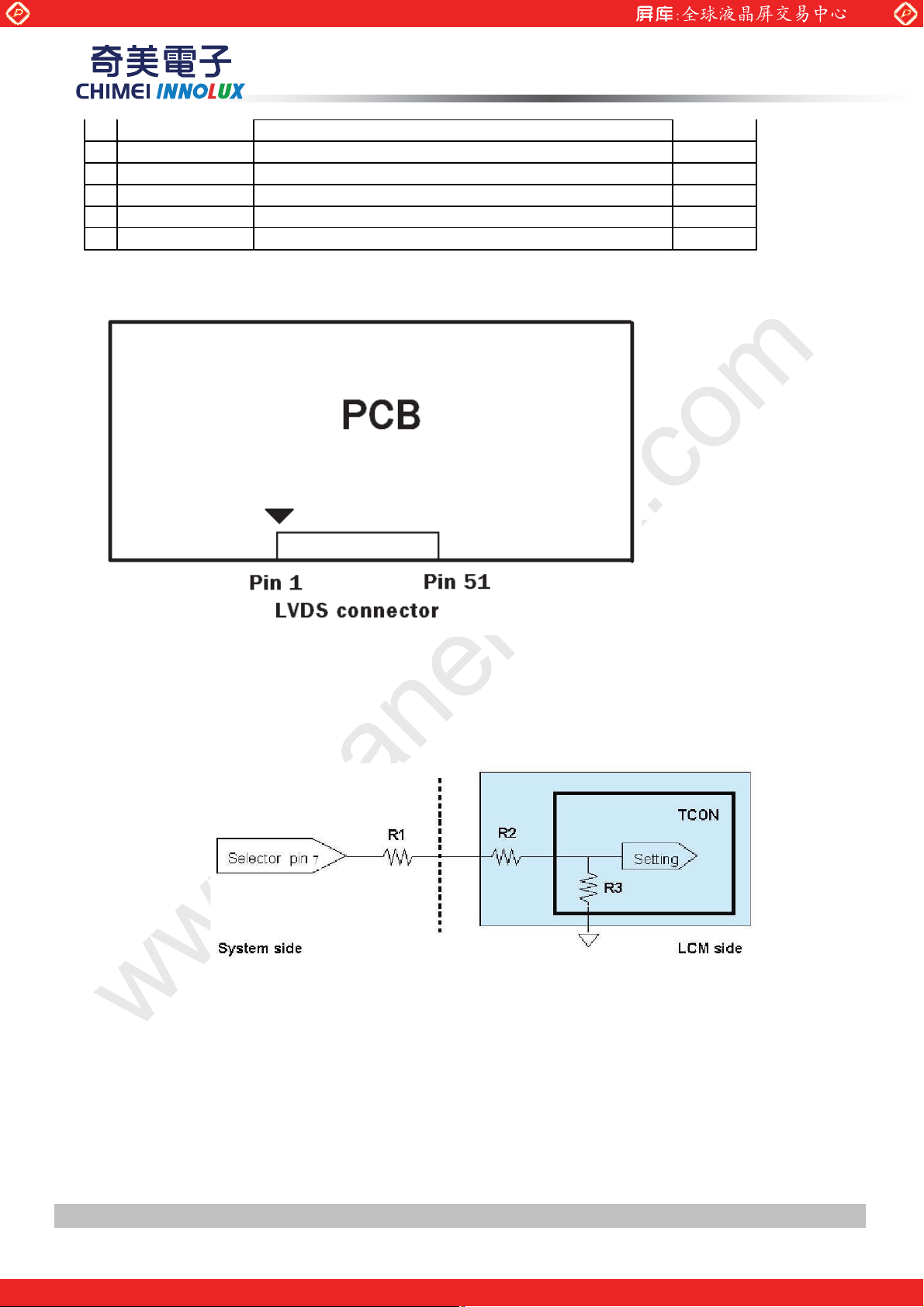
Note (1) LVDS connector pin order defined as follows
www.panelook.com
PRODUCT SPECIFICATION
Note (2) Reserved for internal use. Please leave it open.
Note (3) Low = Open or connect to GND: VESA Format, High = Connect to +3.3V: JEIDA Format.
Note (4) LVDS signal pin connected to the LCM side has the following diagram. R1 in the system side should be
less than 1K Ohm. (Ra < 1K Ohm)
Note (5) Two pixel data send into the module for every clock cycle. The first pixel of the frame is odd pixel and the
second pixel is even pixel.
Version 2.1 14 DateΚΚΚΚ26 Apr 2011
The copyright belongs to CHIMEI InnoLux. Any unauthorized use is prohibited
One step solution for LCD / PDP / OLED panel application: Datasheet, inventory and accessory!
www.panelook.com
Page 15
Global LCD Panel Exchange Center
5.2 BACKLIGHT UNIT
The pin configuration for the housing and the leader wire is shown in the table below.
CN: 51281-0994 (Molex)
Pin № Symbol Feature
1 VLED+ Positive of LED String
2 NC
3 NC
4 N1
5 N2
6 N3
7 NC
8 NC
9 VLED+ Positive of LED String
www.panelook.com
PRODUCT SPECIFICATION
NC
Negative of LED String
NC
Version 2.1 15 DateΚΚΚΚ26 Apr 2011
The copyright belongs to CHIMEI InnoLux. Any unauthorized use is prohibited
One step solution for LCD / PDP / OLED panel application: Datasheet, inventory and accessory!
www.panelook.com
Page 16
Global LCD Panel Exchange Center
G0-EG
0
0
0
p
ORx0
O
p
OB0
CLK
OB0
5.3 BLOCK DIAGRAM OF INTERFACE
www.panelook.com
PRODUCT SPECIFICATION
CNF1
ER0-ER7
E
EB
OR0-OR7
Host
Graphics
x
Controller
TxIN
-EB7
-
-OB7
D
ERx0+
ERx
ERx1+
7
ERx1-
ERx2+
ERx2-
ERx3+
7
ERx3-
100Ө
-
100pF
100Ө
100Ө
100
100Ө
100Ө
100pF
100Ө
100Ө
100pF
100Ө
F
RxOUT
ER0-ER7
E
EB
DE
OR0-OR7
-E
-EB7
-
7
7
-OB7
ECLK+
PLL
100Ө
-
100pF
100Ө
PLL
D
L
Timing
ORx0+
-
ORx1+
ORx1-
ORx2+
Rx2-
ORx3+
ORx3-
100Ө
100pF
100Ө
100Ө
100
100Ө
100Ө
100pF
100Ө
100Ө
100pF
100Ө
F
Controller
OCLK+
PLL
LVDS Transmitter
100Ө
-
100pF
100Ө
LVDS Receiver
PLL
THC63LVDM83A
(LVDF83A)
Version 2.1 16 DateΚΚΚΚ26 Apr 2011
The copyright belongs to CHIMEI InnoLux. Any unauthorized use is prohibited
One step solution for LCD / PDP / OLED panel application: Datasheet, inventory and accessory!
www.panelook.com
Page 17
Global LCD Panel Exchange Center
www.panelook.com
PRODUCT SPECIFICATION
ER0~ER7: Even pixel R data
EG0~EG7: Even pixel G data
EB0~EB7: Even pixel B data
OR0~OR7: Odd pixel R data
OG0~OG7: Odd pixel G data
OB0~OB7: Odd pixel B data
DE: Data enable signal
DCLK: Data clock signal
Note (1) The system must have the transmitter to drive the module.
Note (2) LVDS cable impedance shall be 50 ohms per signal line or about 100 ohms per twist-pair line when it is
used differentially.
Note (3) Two pixel data send into the module for every clock cycle. The first pixel of the frame is odd pixel and the
second pixel is even pixel.
Version 2.1 17 DateΚΚΚΚ26 Apr 2011
The copyright belongs to CHIMEI InnoLux. Any unauthorized use is prohibited
One step solution for LCD / PDP / OLED panel application: Datasheet, inventory and accessory!
www.panelook.com
Page 18
Global LCD Panel Exchange Center
5.4 LVDS INTERFACE
VESA LVDS formatΚ(SELLVDS pin=L or open)
RXCLK
RXCLK
www.panelook.com
PRODUCT SPECIFICATION
Current F\FOH
Current F\FOH
ORX0
ORX0
ORX1
ORX1
ORX2
ORX2
ORX3
ORX3
ERX0
ERX0
ERX1
ERX1
ERX2
ERX2
ERX3
ERX3
JEDIA LVDS formatΚ(SELLVDS pin=H)
RXCLK
RXCLK
ORX0
ORX0
R5G0 R4 R3 R2 R1
R5G0 R4 R3 R2 R1
B0 G5B1
B0 G5B1
R5G0 R4 R3 R2 R1
R5G0 R4 R3 R2 R1
B0 G5B1
B0 G5B1
Current F\FOH
Current F\FOH
R7G2 R6 R5 R4 R3
R7G2 R6 R5 R4 R3
G3 G2G4
G3 G2G4
G3 G2G4
G3 G2G4
R2
R2
R0
R0
G1
G1
B2B4 B3B5VS HSDE
B2B4 B3B5VS HSDE
R6G6 R7G7B7 B6RSVD
R6G6 R7G7B7 B6RSVD
R0
R0
G1
G1
B2B4 B3B5VS HSDE
B2B4 B3B5VS HSDE
R6G6 R7G7B7 B6RSVD
R6G6 R7G7B7 B6RSVD
ORX1
ORX1
ORX2
ORX2
ORX3
ORX3
ERX0
ERX0
ERX1
ERX1
ERX2
ERX2
ERX3
ERX3
B2 G7B3
B2 G7B3
R7G2 R6 R5 R4 R3
R7G2 R6 R5 R4 R3
B2 G7B3
B2 G7B3
G5 G4G6
G5 G4G6
G5 G4G6
G5 G4G6
G3
G3
B4B6 B5B7VS HSDE
B4B6 B5B7VS HSDE
R0G0 R1G1B1 B0RSVD
R0G0 R1G1B1 B0RSVD
R2
R2
G3
G3
B4B6 B5B7VS HSDE
B4B6 B5B7VS HSDE
R0G0 R1G1B1 B0RSVD
R0G0 R1G1B1 B0RSVD
R0~R7: Pixel R Data (7; MSB, 0; LSB)
G0~G7: Pixel G Data (7; MSB, 0; LSB)
B0~B7: Pixel B Data (7; MSB, 0; LSB)
DE : Data enable signal
DCLK : Data clock signal
RSVD : Reserved
Version 2.1 18 DateΚΚΚΚ26 Apr 2011
The copyright belongs to CHIMEI InnoLux. Any unauthorized use is prohibited
One step solution for LCD / PDP / OLED panel application: Datasheet, inventory and accessory!
www.panelook.com
Page 19
Global LCD Panel Exchange Center
www.panelook.com
PRODUCT SPECIFICATION
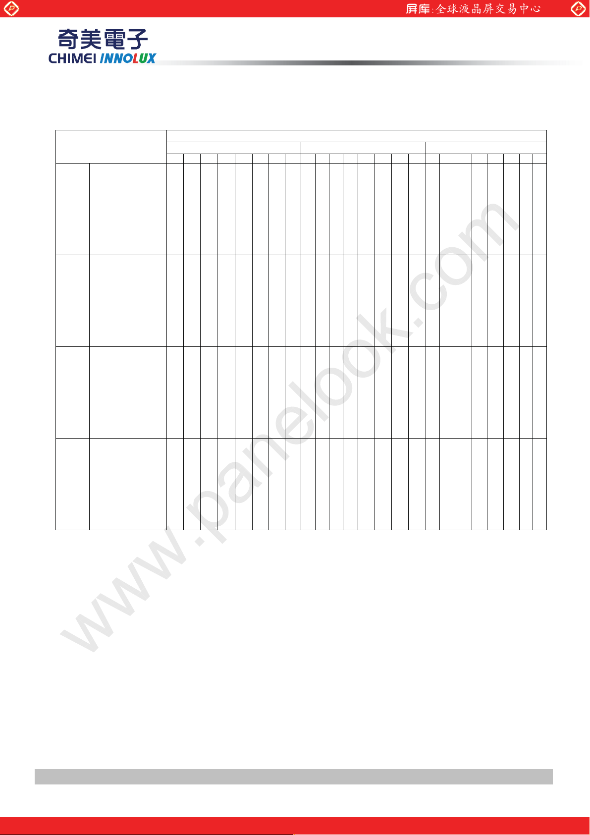
5.5 COLOR DATA INPUT ASSIGNMENT
The brightness of each primary color (red, green and blue) is based on the 8-bit gray scale data input for the color. The
higher the binary input, the brighter the color. The table below provides the assignment of the color versus data input.
Data Signal
Color
R7 R6 R5 R4 R3 R2 R1 R0 G7 G6 G5 G4 G3 G2 G1 G0 B7 B6 B5 B4 B3 B2 B1 B0
Black
Red
Green
Basic
Colors
Gray
Scale
Of
Red
Gray
Scale
Of
Green
Gray
Scale
Of
Blue
Note (1) 0: Low Level Voltage, 1: High Level Voltage
Blue
Cyan
Magenta
Ye ll ow
White
Red (0) / Dark
Red (1)
Red (2)
:
:
Red (253)
Red (254)
Red (255)
Green (0) / Dark
Green (1)
Green (2)
:
:
Green (253)
Green (254)
Green (255)
Blue (0) / Dark
Blue (1)
Blue (2)
:
:
Blue (253)
Blue (254)
Blue (255)
0
0
1
1
0
0
0
0
0
0
1
1
1
1
1
1
0
0
0
0
0
0
:
:
:
:
1
1
1
1
1
1
0
0
0
0
0
0
:
:
:
:
0
0
0
0
0
0
0
0
0
0
0
0
:
:
:
:
0
0
0
0
0
0
Red Green Blue
0
0
0
0
0
0
0
0
0
0
0
0
0
0
0
0
0
0
0
0
0
1
1
1
1
1
1
0
0
0
0
0
0
0
0
0
0
0
0
0
0
0
0
0
0
0
0
0
1
1
1
1
1
1
1
1
0
0
0
0
0
0
0
0
0
0
0
0
0
0
0
0
0
0
0
0
0
1
1
1
1
1
1
1
0
0
0
0
0
0
1
1
1
1
1
1
1
1
1
1
1
1
1
1
1
1
1
1
1
1
1
0
0
0
0
0
0
0
0
1
1
1
1
1
1
1
1
1
1
1
1
1
1
1
1
1
1
1
1
1
0
0
0
0
0
0
0
1
1
1
1
1
1
1
1
1
1
1
1
1
1
1
1
1
1
1
1
1
0
0
0
0
0
0
0
0
0
0
0
0
0
0
0
0
0
0
0
0
0
0
0
0
0
0
1
0
0
0
0
0
0
0
0
0
0
0
0
0
0
0
0
0
0
0
1
0
0
0
0
0
0
0
0
0
0
0
0
0
0
0
0
:
:
:
:
:
:
:
:
:
:
:
:
:
:
:
:
:
:
:
:
:
:
:
:
:
:
:
:
:
:
:
:
:
:
:
:
:
:
:
:
:
:
1
1
1
1
0
1
0
0
0
0
0
0
0
0
0
0
0
0
0
0
0
1
1
1
1
1
0
0
0
0
0
0
0
0
0
0
0
0
0
0
0
0
1
1
1
1
1
1
0
0
0
0
0
0
0
0
0
0
0
0
0
0
0
0
0
0
0
0
0
0
0
0
0
0
0
0
0
0
0
0
0
0
0
0
0
0
0
0
0
0
0
0
0
0
0
0
0
1
0
0
0
0
0
0
0
0
0
0
0
0
0
0
0
0
0
0
0
1
0
0
0
0
0
0
0
0
:
:
:
:
:
:
:
:
:
:
:
:
:
:
:
:
:
:
:
:
:
:
:
:
:
:
:
:
:
:
:
:
:
:
:
:
:
:
:
:
:
:
0
0
0
0
0
0
1
1
1
1
1
1
0
1
0
0
0
0
0
0
0
0
0
0
0
0
0
1
1
1
1
1
1
1
0
0
0
0
0
0
0
0
0
0
0
0
0
0
1
1
1
1
1
1
1
1
0
0
0
0
0
0
0
0
0
0
0
0
0
0
0
0
0
0
0
0
0
0
0
0
0
0
0
0
0
0
0
0
0
0
0
0
0
0
0
0
0
0
0
0
0
0
0
0
0
0
0
0
0
0
0
0
0
0
0
0
0
0
0
0
0
0
0
0
0
1
:
:
:
:
:
:
:
:
:
:
:
:
:
:
:
:
:
:
:
:
:
:
:
:
:
:
:
:
:
:
:
:
:
:
:
:
:
:
:
:
:
:
0
0
0
0
0
0
0
0
0
0
0
0
0
0
1
1
1
1
1
1
0
0
0
0
0
0
0
0
0
0
0
0
0
0
0
1
1
1
1
1
1
1
0
0
0
0
0
0
0
0
0
0
0
0
0
0
1
1
1
1
1
1
1
0
0
0
1
1
1
0
1
0
0
0
:
:
0
0
0
0
0
0
:
:
0
0
0
0
1
0
:
:
1
0
1
Version 2.1 19 DateΚΚΚΚ26 Apr 2011
The copyright belongs to CHIMEI InnoLux. Any unauthorized use is prohibited
One step solution for LCD / PDP / OLED panel application: Datasheet, inventory and accessory!
www.panelook.com
Page 20
Global LCD Panel Exchange Center
6. INTERFACE TIMING
6.1 INPUT SIGNAL TIMING SPECIFICATIONS
(Ta = 25 ± 2 ºC)
The input signal timing specifications are shown as the following table and timing diagram.
Signal Item Symbol Min. Typ. Max. Unit Note
LVDS
Receiver
Clock
Frequency
Input cycle to
cycle jitter
Spread spectrum
modulation range
Spread spectrum
modulation frequency
(=1/TC)
clkin_mod
F
F
www.panelook.com
PRODUCT SPECIFICATION
F
clkin
T
rcl
SSM
60 74.25 80 MHz
ЁЁ
F
-2%
clkin
Ё
Ё
200 ps (3)
F
+2% MHz
clkin
(4)
200 KHz
LVDS
Setup Time Tlvsu 600
ЁЁ
Receiver
Data
Hold Time Tlvhd 600
ЁЁ
Fr5 47 50 53 Hz
Frame Rate
57 60 63 Hz
F
Ver t ical
Active
Display
Term
Total Tv 1115 1125 1135 Th
Display Tvd 1080 1080 1080 Th
r6
Blank Tvb 35 45 55 Th
Horizontal
Active
Display
Term
Total Th 1050 1100 1150 Tc
Display Thd 960 960 960 Tc
Blank Thb 90 140 190 Tc
Note (1) Please make sure the range of frame rate has follow the below equationΚ
Fclkin(max) Fr6 Tv ThЊѼѼ
Fr5 Tv Th Fclkin(min)ѼѼЊ
ps
(5)
ps
Tv=Tvd+Tvb
Th=Thd+Thb
Version 2.1 20 DateΚΚΚΚ26 Apr 2011
The copyright belongs to CHIMEI InnoLux. Any unauthorized use is prohibited
One step solution for LCD / PDP / OLED panel application: Datasheet, inventory and accessory!
www.panelook.com
Page 21

Global LCD Panel Exchange Center
Note (2) This module is operated in DE only mode and please follow the input signal timing diagram belowΚ
DE
T
h
www.panelook.com
PRODUCT SPECIFICATION
INPUT SIGNAL TIMING DIAGRAM
T
v
T
vb
DCLK
T
c
T
DE
DATA
Note (3) The input clock cycle-to-cycle jitter is defined as below figures. Trcl = I T1 – TI
hb
Valid display data (960)
T
hd
Version 2.1 21 DateΚΚΚΚ26 Apr 2011
The copyright belongs to CHIMEI InnoLux. Any unauthorized use is prohibited
One step solution for LCD / PDP / OLED panel application: Datasheet, inventory and accessory!
www.panelook.com
Page 22

Global LCD Panel Exchange Center
Note (4) The SSCG (Spread spectrum clock generator) is defined as below figures.
www.panelook.com
PRODUCT SPECIFICATION
Note (5) The LVDS timing diagram and setup/hold time is defined and showing as the following figures.
LVDS RECEIVER INTERFACE TIMING DIAGRAM
Tc
RXCLK+/-
RXn+/-
Tlvsu
Tlvhd
1T
14
3T
14
5T
14
7T
14
9T
14
11T
14
13T
14
Version 2.1 22 DateΚΚΚΚ26 Apr 2011
The copyright belongs to CHIMEI InnoLux. Any unauthorized use is prohibited
One step solution for LCD / PDP / OLED panel application: Datasheet, inventory and accessory!
www.panelook.com
Page 23

Global LCD Panel Exchange Center
6.2 POWER ON/OFF SEQUENCE
(Ta = 25 ± 2 ºC)
To prevent a latch-up or DC operation of LCD module, the power on/off sequence should be as the diagram
below.
0V
0.5ЉT1Љ10ms
0ЉT2Љ50ms
0ЉT3Љ50ms
500ms ЉT4
LVDS Signals
0V
www.panelook.com
0.1V
CC
Power On
PRODUCT SPECIFICATION
0.1V
cc
T
T
1
T
2
VALID
3
T
4
Power Off
0ЉT7ЉT2
0ЉT8ЉT3
T
7
T
8
Option Signals
(SELLVDS)
Backlight (Recommended)
500msЉT5
100msЉT6
50%
T
5
Power ON/OFF Sequence
50%
6
T
Note (1) The supply voltage of the external system for the module input should follow the definition of Vcc.
Note (2) Apply the lamp voltage within the LCD operation range. When the backlight turns on before the LCD
operation or the LCD turns off before the backlight turns off, the display may momentarily become
abnormal screen.
Note (3) In case of VCC is in off level, please keep the level of input signals on the low or high impedance.
Note (4) T4 should be measured after the module has been fully discharged between power off and on period.
Note (5) Interface signal shall not be kept at high impedance when the power is on.
Version 2.1 23 DateΚΚΚΚ26 Apr 2011
The copyright belongs to CHIMEI InnoLux. Any unauthorized use is prohibited
One step solution for LCD / PDP / OLED panel application: Datasheet, inventory and accessory!
www.panelook.com
Page 24

Global LCD Panel Exchange Center
7. OPTICAL CHARACTERISTICS
7.1 TEST CONDITIONS
Item Symbol Value Unit
www.panelook.com
PRODUCT SPECIFICATION
Ambient Temperature Ta
Ambient Humidity Ha
Supply Voltage VCC 12 V V
Input Signal According to typical value in "3. ELECTRICAL CHARACTERISTICS"
LED Current I
The LCD module should be stabilized at given temperature for 1 hour to avoid abrupt temperature change during
measuring in a windless room.
L
25±2
50±10
120 ± 7.2
к
%RH
mA
Version 2.1 24 DateΚΚΚΚ26 Apr 2011
The copyright belongs to CHIMEI InnoLux. Any unauthorized use is prohibited
One step solution for LCD / PDP / OLED panel application: Datasheet, inventory and accessory!
www.panelook.com
Page 25

Global LCD Panel Exchange Center
7.2 OPTICAL SPECIFICATIONS
The relative measurement methods of optical characteristics are shown in 7.2. The following items should be
measured under the test conditions described in 7.1 and stable environment shown in 7.1.
Item Symbol Condition Min. Typ. Max. Unit Note
Contrast Ratio CR 3000 4000 - - (2)
www.panelook.com
PRODUCT SPECIFICATION
Response Time (VA)
Center Luminance of White LC -- 450 -
White Variation
Cross Talk CT - - 4 % (5)
Red
Green
Color
Chromaticity
Blue
White
Color Gamut C.G
Gray to
gray
δW
Rx 0.645 -
Ry 0.325 -
Gx 0.300 -
Gy 0.630 -
Bx 0.147 -
By 0.065 -
Wx 0.280 -
Wy
θx=0°, θy =0°
Viewing angle
at normal direction
- 8.5 17 ms (3)
cd/m
2
- - 1.3 - (6)
Typ.
-0.03
0.290
- 72 - % NTSC
Typ.
+0.03
-
(4)
-
Viewing
Angle
Horizontal
Ver t ical
θx+
θx-
θY+
θY-
CR≥20 (VA)
CR≥10 (TN)
80 88 -
80 88 -
80 88 80 88 -
Deg. (1)
Version 2.1 25 DateΚΚΚΚ26 Apr 2011
The copyright belongs to CHIMEI InnoLux. Any unauthorized use is prohibited
One step solution for LCD / PDP / OLED panel application: Datasheet, inventory and accessory!
www.panelook.com
Page 26

Global LCD Panel Exchange Center
T
Note (1) Definition of Viewing Angle (θx, θy) :
Viewing angles are measured by Conoscope Cono-80 ( or Eldim EZ-Contrast 160R )
www.panelook.com
PRODUCT SPECIFICATION
Normal
θx =θy = 0º
θx- = 90º
x-
6 o’clock
y-
θy- = 90º
Note (2) Definition of Contrast Ratio (CR) :
The contrast ratio can be calculated by the following expression.
Contrast Ratio (CR) =
L255: Luminance of gray level 255
L 0: Luminance of gray level 0
CR = CR (5), where CR (X) is corresponding to the Contrast Ratio of the point X at the figure in Note
θy-
θx−
θy+
θx+
12 o’clock direction
θy + = 90º
x
+
θx+ = 90º
L255of LuminanceSurface
L0 of LuminanceSurface
(6).
Note (3) Definition of Gray-to-Gray Switching Time:
100%
90%
Optical
Response
10%
0%
Gray to gray
switching time
The driving signal means the signal of gray level 0, 31, 63, 95, 127, 159, 191, 223 and 255.
Gray to gray average time means the average switching time of gray level 0, 31, 63, 95, 127, 159, 191,
223 and 255 to each other.
Gray to gray
ime
switching time
Version 2.1 26 DateΚΚΚΚ26 Apr 2011
The copyright belongs to CHIMEI InnoLux. Any unauthorized use is prohibited
One step solution for LCD / PDP / OLED panel application: Datasheet, inventory and accessory!
www.panelook.com
Page 27

Global LCD Panel Exchange Center
A
(
)
A
(
)
(
)
A
(
)
A
(
)
(
)
Note (4) Definition of Luminance of White (LC):
Measure the luminance of gray level 255 at center point and 5 points
L
= L (5), where L (X) is corresponding to the luminance of the point X at the figure in Note (6).
C
Note (5) Definition of Cross Talk (CT):
www.panelook.com
PRODUCT SPECIFICATION
CT = | Y
– YA | / YA× 100 (%)
B
Where:
Y
= Luminance of measured location without gray level 0 pattern (cd/m2)
A
Y
= Luminance of measured location with gray level 0 pattern (cd/m2)
B
ctive Area
(0, 0)
Y
(D/2,W/8)
A, U
0, 0
(D/4,W/4)
Gray 128
Y
(D/8,W/2)
A, L
Y
= Luminance of measured location without gray level 255 pattern (cd/m2)
Y
A
Y
= Luminance of measured location with gray level 255 pattern (cd/m2)
B
Y
(D/2,7W/8)
A, D
(7D/8,W/2)
A, R
D, W
(D/8,W/2)
Y
B, L
ctive Area
Y
Gray 0
Y
(D/2,W/8)
B, U
Y
(3D/4,3W/4)
(D/2,7W/8)
B, D
(7D/8,W/2)
B, R
D, W
(0, 0)
(D/8,W/2)
Y
A, L
ctive Area
Y
Gray 128
Y
(D/2,W/8)
A, U
Y
(D/2,7W/8)
A, D
(7D/8,W/2)
A, R
D, W
0, 0
(D/8,W/2)
Y
B, L
(D/4,W/4)
ctive Area
Y
Gray 255
Y
(D/2,W/8)
B, U
Y
(3D/4,3W/4)
(D/2,7W/8)
B, D
(7D/8,W/2)
B, R
D, W
Version 2.1 27 DateΚΚΚΚ26 Apr 2011
The copyright belongs to CHIMEI InnoLux. Any unauthorized use is prohibited
One step solution for LCD / PDP / OLED panel application: Datasheet, inventory and accessory!
www.panelook.com
Page 28

Global LCD Panel Exchange Center
Note (6) Definition of White Variation (δW):
Measure the luminance of gray level 255 at 5 points
δW = Maximum [L (1), L (2), L (3), L (4), L (5)] / Minimum [L (1), L (2), L (3), L (4), L (5)]
www.panelook.com
PRODUCT SPECIFICATION
Horizontal Line
D
D/4 D/2 3D/4
Vertical Line
W
W/4
W/2
1 2
5
3 4
Active Area
: Test Point
X=1 to 5
Version 2.1 28 DateΚΚΚΚ26 Apr 2011
The copyright belongs to CHIMEI InnoLux. Any unauthorized use is prohibited
One step solution for LCD / PDP / OLED panel application: Datasheet, inventory and accessory!
www.panelook.com
Page 29

Global LCD Panel Exchange Center
www.panelook.com
PRODUCT SPECIFICATION
8. PRECAUTIONS
8.1 ASSEMBLY AND HANDLING PRECAUTIONS
[ 1 ] Do not apply rough force such as bending or twisting to the module during assembly.
[ 2 ] It is recommended to assemble or to install a module into the user’s system in clean working areas. The
dust and oil may cause electrical short or worsen the polarizer.
[ 3 ] Do not apply pressure or impulse to the module to prevent the damage of LCD panel and backlight.
[ 4 ] Always follow the correct power-on sequence when the LCD module is turned on. This can prevent the
damage and latch-up of the CMOS LSI chips.
[ 5 ] Do not plug in or pull out the I/F connector while the module is in operation.
[ 6 ] Do not disassemble the module.
[ 7 ] Use a soft dry cloth without chemicals for cleaning, because the surface of polarizer is very soft and easily
scratched.
[ 8 ] Moisture can easily penetrate into LCD module and may cause the damage during operation.
[ 9 ] High temperature or humidity may deteriorate the performance of LCD module. Please store LCD modules
in the specified storage conditions.
[ 10 ] When ambient temperature is lower than 10ºC, the display quality might be reduced. For example, the
response time will become slow.
8.2 SAFETY PRECAUTIONS
[ 1 ] Do not disassemble the module or insert anything into the Backlight unit.
[ 2 ] If the liquid crystal material leaks from the panel, it should be kept away from the eyes or mouth. In case of
contact with hands, skin or clothes, it has to be washed away thoroughly with soap.
[ 3 ] After the module’s end of life, it is not harmful in case of normal operation and storage.
8.3 STORAGE PRECAUTIONS
When storing module as spares for a long time, the following precaution is necessary.
[1] Do not leave the module in high temperature, and high humidity for a long time.
It is highly recommended to store the module with temperature from 0 to 35к at normal humidity without
condensation.
[2] The module shall be stored in dark place. Do not store the TFT-LCD module in direct sunlight or fluorescent
light.
Version 2.1 29 DateΚΚΚΚ26 Apr 2011
The copyright belongs to CHIMEI InnoLux. Any unauthorized use is prohibited
One step solution for LCD / PDP / OLED panel application: Datasheet, inventory and accessory!
www.panelook.com
Page 30

Global LCD Panel Exchange Center
9. DEFINITION OF LABELS
9.1 CMI MODULE LABEL
The barcode nameplate is pasted on each module as illustration, and its definitions are as following explanation.
www.panelook.com
PRODUCT SPECIFICATION
CHI MEI
OPTOELECTRONICS
CHI MEI
OPTOELECTRONICS
Model Name: V315H4-LE3
Revision: Rev. XX, for example: A0, A1… B1, B2… or C1, C2…etc.
Serial ID: X X X X X X X Y M D L N N N N
V315H4 –LE3 Rev. XX
X X X X X X X Y M D L N N N N
V315H4 –LE3 Rev. XX
X X X X X X X Y M D L N N N N
Serial No.
E207943
MADE IN TAIWAN
GEMN
RoHS
MADE IN CHINA
LEOO(or CAPG or CANO)
RoHS
Product Line
Year, Month, Date
CMI Internal Use
CMI Internal Use
Revision
Serial ID includes the information as below:
Manufactured Date:
Year : 2001=1, 2002=2, 2003=3, 2004=4…2010=0, 2011=1, 2012=2…
Month: 1~9, A~C, for Jan. ~ Dec.
Day: 1~9, A~Y, for 1st to 31st, exclude I ,O, and U.
Revision Code : Cover all the change
Serial No. : Manufacturing sequence of product
Product Line : 1 → Line1, 2 → Line 2, …etc.
CMI Internal Use
Version 2.1 30 DateΚΚΚΚ26 Apr 2011
The copyright belongs to CHIMEI InnoLux. Any unauthorized use is prohibited
One step solution for LCD / PDP / OLED panel application: Datasheet, inventory and accessory!
www.panelook.com
Page 31

Global LCD Panel Exchange Center
10. MECHANICAL CHARACTERISTIC
www.panelook.com
PRODUCT SPECIFICATION
Version 2.1 31 DateΚΚΚΚ26 Apr 2011
The copyright belongs to CHIMEI InnoLux. Any unauthorized use is prohibited
One step solution for LCD / PDP / OLED panel application: Datasheet, inventory and accessory!
www.panelook.com
Page 32

Global LCD Panel Exchange Center
www.panelook.com
PRODUCT SPECIFICATION
Version 2.1 32 DateΚΚΚΚ26 Apr 2011
The copyright belongs to CHIMEI InnoLux. Any unauthorized use is prohibited
One step solution for LCD / PDP / OLED panel application: Datasheet, inventory and accessory!
www.panelook.com
Page 33

Global LCD Panel Exchange Center
MODEL NO.: V315H4
www.panelook.com
PRODUCT SPECIFICATION
□ Tentative Specification
□Preliminary Specification
■ Approval Specification
SUFFIX: LE3
Customer:
APPROVED BY SIGNATURE
Name / Title
Note
Approved By Checked By Prepared By
Chao-Chun Chung Ken Wu Carlos Lee
Version 2.1 1 DateΚΚΚΚ26 Apr 2011
The copyright belongs to CHIMEI InnoLux. Any unauthorized use is prohibited
One step solution for LCD / PDP / OLED panel application: Datasheet, inventory and accessory!
www.panelook.com
Page 34

Global LCD Panel Exchange Center
www.panelook.com
PRODUCT SPECIFICATION
CONTENTS
1. GENERAL DESCRIPTION ......................................................................................................................................................... 5
1.1 OVERVIEW ..........................................................................................................................................................5
1.2 FEATURES ..........................................................................................................................................................5
1.3 APPLICATION...................................................................................................................................................... 5
1.4 GENERAL SPECIFICATIONS .............................................................................................................................5
1.5 MECHANICAL SPECIFICATIONS....................................................................................................................... 5
2. ABSOLUTE MAXIMUM RATINGS .......................................................................................................................................... 6
2.1 ABSOLUTE RATINGS OF ENVIRONMENT ........................................................................................................ 6
2.2 PACKAGE STORAGE.......................................................................................................................................... 7
2.3 ELECTRICAL ABSOLUTE RATINGS .................................................................................................................. 7
3. ELECTRICAL CHARACTERISTICS ......................................................................................................................................... 8
3.1 TFT LCD MODULE ..............................................................................................................................................8
3.2 BACKLIGHT CONNECTOR PIN CONFIGURATION......................................................................................... 11
4. BLOCK DIAGRAM OF INTERFACE ...................................................................................................................................... 12
4.1 TFT LCD MODULE ............................................................................................................................................12
5. INPUT TERMINAL PIN ASSIGNMENT ................................................................................................................................ 13
5.1 TFT LCD Module Input....................................................................................................................................... 13
5.2 BACKLIGHT UNIT.............................................................................................................................................. 15
5.3 BLOCK DIAGRAM OF INTERFACE.................................................................................................................. 16
5.4 LVDS INTERFACE ............................................................................................................................................. 18
5.5 COLOR DATA INPUT ASSIGNMENT ................................................................................................................ 19
6. INTERFACE TIMING................................................................................................................................................................ 20
6.1 INPUT SIGNAL TIMING SPECIFICATIONS...................................................................................................... 20
6.2 POWER ON/OFF SEQUENCE..........................................................................................................................23
7. OPTICAL CHARACTERISTICS............................................................................................................................................... 24
7.1 TEST CONDITIONS...........................................................................................................................................24
7.2 OPTICAL SPECIFICATIONS .............................................................................................................................25
8. PRECAUTIONS .......................................................................................................................................................................... 29
8.1 ASSEMBLY AND HANDLING PRECAUTIONS .................................................................................................29
8.2 SAFETY PRECAUTIONS ..................................................................................................................................29
Version 2.1 2 DateΚΚΚΚ26 Apr 2011
The copyright belongs to CHIMEI InnoLux. Any unauthorized use is prohibited
One step solution for LCD / PDP / OLED panel application: Datasheet, inventory and accessory!
www.panelook.com
Page 35

Global LCD Panel Exchange Center
www.panelook.com
PRODUCT SPECIFICATION
8.3 STORAGE PRECAUTIONS............................................................................................................................... 29
9. DEFINITION OF LABELS......................................................................................................................................................... 30
9.1 CMI MODULE LABEL ........................................................................................................................................30
10. MECHANICAL CHARACTERISTIC .................................................................................................................................... 31
Version 2.1 3 DateΚΚΚΚ26 Apr 2011
The copyright belongs to CHIMEI InnoLux. Any unauthorized use is prohibited
One step solution for LCD / PDP / OLED panel application: Datasheet, inventory and accessory!
www.panelook.com
Page 36

Global LCD Panel Exchange Center
Version Date Page(New) Section Description
Ver. 0. 0
Ver. 1. 0
Ver. 2. 0
Ver. 2. 1
Dec. 08, 2010
Dec.28, 2010
Jan. 14, 2011
Apr. 26, 2011
All
All
All
15
www.panelook.com
PRODUCT SPECIFICATION
REVISION HISTORY
All
All
All
5.2
The tentative specification was first issued.
The preliminary specification was first issued.
The Approval Specification was first issued.
Modify PIN ASSIGNMENT
Version 2.1 4 DateΚΚΚΚ26 Apr 2011
The copyright belongs to CHIMEI InnoLux. Any unauthorized use is prohibited
One step solution for LCD / PDP / OLED panel application: Datasheet, inventory and accessory!
www.panelook.com
Page 37

Global LCD Panel Exchange Center
1. GENERAL DESCRIPTION
1.1 OVERVIEW
V315H4-LE3 is a TFT Liquid Crystal Display module with LED Backlight unit and 2ch-LVDS interface. The display
diagonal is 31.5”. This module supports 1920 x 1080 Full HDTV format and can display 16.7M colors (8-bit). The
converter module for backlight isn’t built-in.
1.2 FEATURES
Ё High contrast ratio (4000:1)
Ё Fast response time (8.5ms)
Ё High color saturation (NTSC 72%)
Ё Full HDTV (1920 x 1080 pixels) resolution, true HDTV format
Ё DE (Data Enable) only mode
www.panelook.com
PRODUCT SPECIFICATION
Ё LVDS (Low Voltage Differential Signaling) interface
Ё Viewing Angle : 176(H)/176(V) (CR>20) MVA Technology
Ё RoHs compliance
1.3 APPLICATION
Ё TFT LCD TVs
Ё Multi-Media Displays
1.4 GENERAL SPECIFICATIONS
Item Specification Unit Note
Active Area 697.92(H) x 392.58 (V) mm (1)
Driver Element a-si TFT active matrix - -
Pixel Number 1920 x W. R.G.B. x 1080 pixel -
Pixel Pitch(Sub Pixel) 0.18175 (H) x 0.18175 (V) mm -
Pixel Arrangement wRGB square - -
Display Colors 16.7M color -
Display Operation Mode Transmissive mode / Normally Black - -
Surface Treatment Anti-Glare coating (Haze 14%) / Hard Coating (3H) - (2)
Note (1) Please refer to the attached drawings for more information about the front and back outlines.
Note (2) The spec. of the surface treatment is temporarily for this phase. CMI reserves the rights to change this feature.
1.5 MECHANICAL SPECIFICATIONS
Item Min. Typ. Max. Unit Note
Horizontal (H) 740.4 741.4 742.4 mm Module size
Module Size
Weight - 3710 - g -
Vertical (V) 435.0 435.8 436.6 mm
Depth (D) 8.9 9.4 9.9 mm To rear
Version 2.1 5 DateΚΚΚΚ26 Apr 2011
The copyright belongs to CHIMEI InnoLux. Any unauthorized use is prohibited
One step solution for LCD / PDP / OLED panel application: Datasheet, inventory and accessory!
www.panelook.com
Page 38

Global LCD Panel Exchange Center
2. ABSOLUTE MAXIMUM RATINGS
2.1 ABSOLUTE RATINGS OF ENVIRONMENT
Item Symbol
Storage Temperature TST -20 +60 ºC (1)
Operating Ambient Temperature TOP 0 50 ºC (1), (2)
Shock (Non-Operating) SNOP - 50 G (3), (5)
Vibration (Non-Operating) VNOP - 1.0 G (4), (5)
Note (1) Temperature and relative humidity range is shown in the figure below.
(a) 90 %RH Max. (Ta Љ 40 ºC).
(b) Wet-bulb temperature should be 39 ºC Max. (Ta > 40 ºC).
(c) No condensation.
Note (2) The maximum operating temperature is based on the test condition that the surface temperature of
www.panelook.com
PRODUCT SPECIFICATION
Value
Min. Max.
Unit Note
display area is less than or equal to 65 ºC with LCD module alone in a temperature controlled chamber.
Thermal management should be considered in final product design to prevent the surface temperature
of display area from being over 65 ºC. The range of operating temperature may degrade in case of
improper thermal management in final product design.
Note (3) 11 ms, half sine wave, 1 time for ± X, ± Y, ± Z.
Note (4) 10 ~ 200 Hz, 10 min, 1 time each X, Y, Z.
Note (5) At testing Vibration and Shock, the fixture in holding the module has to be hard and rigid enough so that
the module would not be twisted or bent by the fixture.
Version 2.1 6 DateΚΚΚΚ26 Apr 2011
The copyright belongs to CHIMEI InnoLux. Any unauthorized use is prohibited
One step solution for LCD / PDP / OLED panel application: Datasheet, inventory and accessory!
www.panelook.com
Page 39

Global LCD Panel Exchange Center
2.2 PACKAGE STORAGE
When storing modules as spares for a long time, the following precaution is necessary.
(a) Do not leave the module in high temperature, and high humidity for a long time, It is highly recommended to
store the module with temperature from 0 to 35 к at normal humidity without condensation.
(b) The module shall be stored in dark place. Do not store the TFT-LCD module in direct sunlight or fluorescent
light.
2.3 ELECTRICAL ABSOLUTE RATINGS
2.3.1 TFT LCD MODULE
Item Symbol
Power Supply Voltage Vcc -0.3 13.5 V
Input Signal Voltage VIN -0.3 3.6 V
www.panelook.com
PRODUCT SPECIFICATION
Value
Min. Max.
Unit Note
(1)
Version 2.1 7 DateΚΚΚΚ26 Apr 2011
The copyright belongs to CHIMEI InnoLux. Any unauthorized use is prohibited
One step solution for LCD / PDP / OLED panel application: Datasheet, inventory and accessory!
www.panelook.com
Page 40

Global LCD Panel Exchange Center
3. ELECTRICAL CHARACTERISTICS
3.1 TFT LCD MODULE
(Ta = 25 ± 2 ºC)
Parameter Symbol
Power Supply Voltage VCC 10.8 12 13.2 V (1)
www.panelook.com
PRODUCT SPECIFICATION
Value
Unit Note
Min. Typ. Max.
Rush Current I
White Pattern
Power consumption
Horizontal Stripe
Black Pattern
White Pattern
Power Supply Current
Horizontal Stripe
Black Pattern
Differential Input High
Threshold Voltage
Differential Input Low
Threshold Voltage
LVDS
interface
Common Input Voltage VCM 1.0 1.2 1.4 V
Differential input voltage
(single-end)
Terminating Resistor R
RUSH
ЁЁ
Ё
P
T
Ё
Ё
ЁЁ
ЁЁ
ЁЁ
V
V
|V
LVT H
LVT L
ID
T
+100
ЁЁ
| 200
Ё
3.7 A (2)
6.72 8.16 W
7.92 9.84 W
4.8 5.76 W
0.56 0.68 A
0.66 0.82 A
0.4 0.48 A
ЁЁ
mV
-100 mV
Ё
100
600 mV
Ё
ohm
(3)
(4)
(5)
CMIS
interface
Input High Threshold Voltage VIH 2.7
Input Low Threshold Voltage V
0
IL
Ё
Ё
3.3 V
0.7 V
Note (1) The module should be always operated within the above ranges.
Version 2.1 8 DateΚΚΚΚ26 Apr 2011
The copyright belongs to CHIMEI InnoLux. Any unauthorized use is prohibited
One step solution for LCD / PDP / OLED panel application: Datasheet, inventory and accessory!
www.panelook.com
Page 41

Global LCD Panel Exchange Center
Note (2) Measurement ConditionsΚ
www.panelook.com
PRODUCT SPECIFICATION
GND
Vcc rising time is 470us
Vcc
0.9Vcc
0.1Vcc
470us
Version 2.1 9 DateΚΚΚΚ26 Apr 2011
The copyright belongs to CHIMEI InnoLux. Any unauthorized use is prohibited
One step solution for LCD / PDP / OLED panel application: Datasheet, inventory and accessory!
www.panelook.com
Page 42

Global LCD Panel Exchange Center
www.panelook.com
PRODUCT SPECIFICATION
Note (3) The Specified Power consumption is under a,b,c pattern.
Note (4) The Specified power supply current is under the conditions at Vcc = 12 V, Ta = 25 ± 2 ºC, f
whereas a power dissipation check pattern below is displayed.
a. White Pattern
Active Area
c. Horizontal Pattern
b. Black Pattern
Active Area
= 60 Hz,
v
Note (5) The LVDS input characteristics are as follows :
Version 2.1 10 DateΚΚΚΚ26 Apr 2011
The copyright belongs to CHIMEI InnoLux. Any unauthorized use is prohibited
One step solution for LCD / PDP / OLED panel application: Datasheet, inventory and accessory!
www.panelook.com
Page 43

Global LCD Panel Exchange Center
www.panelook.com
3.2 BACKLIGHT CONNECTOR PIN CONFIGURATION
PRODUCT SPECIFICATION
3.2.1 LED LIGHT BAR CHARACTERISTICS (
Ta = 25 ± 2 ºC)
The backlight unit contains 2 pcs light bar.
Parameter Symbol
Total Current (6 String) If
One String Current I
LED Forward Voltage V
One String Voltage V
One String Voltage Variation
ϦV
Life time -
Min. Typ. Max.
- 720 763.2
L
f
W
- - 2
W
- 120 127.2
3.0 3.25 3.5
51 - 59.5
30,000 - -
Value
Unit Note
mA
mA
I
V
DC
I
V
DC
V
Hrs (1)
Note (1) The lifetime is defined as the time which luminance of the LED decays to 50% compared to the
initial value, Operating condition: Continuous operating at Ta = 25±2 , Iк
=120mA.
L
=120mA
L
=120mA
L
Version 2.1 11 DateΚΚΚΚ26 Apr 2011
The copyright belongs to CHIMEI InnoLux. Any unauthorized use is prohibited
One step solution for LCD / PDP / OLED panel application: Datasheet, inventory and accessory!
www.panelook.com
Page 44

Global LCD Panel Exchange Center
)
4. BLOCK DIAGRAM OF INTERFACE
4.1 TFT LCD MODULE
ER 0+/ER 1+/ER 2+/ER 3+/ER CLK+/-
OR 0+/OR 1+/OR 2+/OR 3+/OR CLK+/-
(FI-RE51S-HF (JAE)) or equivalent
INPUT CONNECTOR
FRAME
BUFFER
MEMC
SELLVDS
www.panelook.com
PRODUCT SPECIFICATION
SCAN DRIVER
TFT LCD PANEL
(1920x2x1080 x2)
TIMING
CONTROLLER
Data Driver (mini-LVDS
VIN
GND
DC/DC CONVERTER
& REFERENCE VOLTAGE
GENERATOR
CN2:51281-1094 (Molex) or equivalent
LED
BACKLIGHT
UNIT
Version 2.1 12 DateΚΚΚΚ26 Apr 2011
The copyright belongs to CHIMEI InnoLux. Any unauthorized use is prohibited
One step solution for LCD / PDP / OLED panel application: Datasheet, inventory and accessory!
www.panelook.com
Page 45

Global LCD Panel Exchange Center
www.panelook.com
PRODUCT SPECIFICATION
5. INPUT TERMINAL PIN ASSIGNMENT
5.1 TFT LCD Module Input
CNF1 Connector Part No.: JAE Taiwan FI-RE51S-HF or equivalent.
Pin Name Description Note
1 GND Ground
2 N.C. No Connection
3 N.C. No Connection
4 N.C. No Connection
5 N.C. No Connection
6 N.C. No Connection
7 SELLVDS LVDS data format Selection (3) (4)
8 N.C. No Connection
9 N.C. No Connection
10 N.C. No Connection
11 GND Ground
12 ERX0- Even pixel Negative LVDS differential data input. Channel 0
13 ERX0+ Even pixel Positive LVDS differential data input. Channel 0
14 ERX1- Even pixel Negative LVDS differential data input. Channel 1
15 ERX1+ Even pixel Positive LVDS differential data input. Channel 1
16 ERX2- Even pixel Negative LVDS differential data input. Channel 2
17 ERX2+ Even pixel Positive LVDS differential data input. Channel 2
18 GND Ground
19 ECLK- Even pixel Negative LVDS differential clock input.
20 ECLK+ Even pixel Positive LVDS differential clock input.
21 GND Ground
22 ERX3- Even pixel Negative LVDS differential data input. Channel 3
23 ERX3+ Even pixel Positive LVDS differential data input. Channel 3
24 N.C. No Connection
25 N.C. No Connection
26 GND Ground
27 GND Ground
28 ORX0- Odd pixel Negative LVDS differential data input. Channel 0
29 ORX0+ Odd pixel Positive LVDS differential data input. Channel 0
30 ORX1- Odd pixel Negative LVDS differential data input. Channel 1
31 ORX1+ Odd pixel Positive LVDS differential data input. Channel 1
32 ORX2- Odd pixel Negative LVDS differential data input. Channel 2
33 ORX2+ Odd pixel Positive LVDS differential data input. Channel 2
34 GND Ground
35 OCLK- Odd pixel Negative LVDS differential clock input.
36 OCLK+ Odd pixel Positive LVDS differential clock input.
37 GND Ground
38 ORX3- Odd pixel Negative LVDS differential data input. Channel 3
39 ORX3+ Odd pixel Positive LVDS differential data input. Channel 3
40 N.C. No Connection
41 N.C. No Connection
42 GND Ground
43 GND Ground
44 GND Ground
45 GND Ground
(2)
(2)
(5)
(5)
(5)
(2)
(5)
(5)
(5)
(2)
Version 2.1 13 DateΚΚΚΚ26 Apr 2011
The copyright belongs to CHIMEI InnoLux. Any unauthorized use is prohibited
One step solution for LCD / PDP / OLED panel application: Datasheet, inventory and accessory!
www.panelook.com
Page 46

Global LCD Panel Exchange Center
46 GND Ground
47 N.C. No Connection (2)
48 VCC +12V power supply
49 VCC +12V power supply
50 VCC +12V power supply
51 VCC +12V power supply
Note (1) LVDS connector pin order defined as follows
www.panelook.com
PRODUCT SPECIFICATION
Note (2) Reserved for internal use. Please leave it open.
Note (3) Low = Open or connect to GND: VESA Format, High = Connect to +3.3V: JEIDA Format.
Note (4) LVDS signal pin connected to the LCM side has the following diagram. R1 in the system side should be
less than 1K Ohm. (Ra < 1K Ohm)
Note (5) Two pixel data send into the module for every clock cycle. The first pixel of the frame is odd pixel and the
second pixel is even pixel.
Version 2.1 14 DateΚΚΚΚ26 Apr 2011
The copyright belongs to CHIMEI InnoLux. Any unauthorized use is prohibited
One step solution for LCD / PDP / OLED panel application: Datasheet, inventory and accessory!
www.panelook.com
Page 47

Global LCD Panel Exchange Center
5.2 BACKLIGHT UNIT
The pin configuration for the housing and the leader wire is shown in the table below.
CN: 51281-0994 (Molex)
Pin № Symbol Feature
1 VLED+ Positive of LED String
2 NC
3 NC
4 N1
5 N2
6 N3
7 NC
8 NC
9 VLED+ Positive of LED String
www.panelook.com
PRODUCT SPECIFICATION
NC
Negative of LED String
NC
Version 2.1 15 DateΚΚΚΚ26 Apr 2011
The copyright belongs to CHIMEI InnoLux. Any unauthorized use is prohibited
One step solution for LCD / PDP / OLED panel application: Datasheet, inventory and accessory!
www.panelook.com
Page 48

Global LCD Panel Exchange Center
G0-EG
0
0
0
p
ORx0
O
p
OB0
CLK
OB0
5.3 BLOCK DIAGRAM OF INTERFACE
www.panelook.com
PRODUCT SPECIFICATION
CNF1
ER0-ER7
E
EB
OR0-OR7
Host
Graphics
x
Controller
TxIN
-EB7
-
-OB7
D
ERx0+
ERx
ERx1+
7
ERx1-
ERx2+
ERx2-
ERx3+
7
ERx3-
100Ө
-
100pF
100Ө
100Ө
100
100Ө
100Ө
100pF
100Ө
100Ө
100pF
100Ө
F
RxOUT
ER0-ER7
E
EB
DE
OR0-OR7
-E
-EB7
-
7
7
-OB7
ECLK+
PLL
100Ө
-
100pF
100Ө
PLL
D
L
Timing
ORx0+
-
ORx1+
ORx1-
ORx2+
Rx2-
ORx3+
ORx3-
100Ө
100pF
100Ө
100Ө
100
100Ө
100Ө
100pF
100Ө
100Ө
100pF
100Ө
F
Controller
OCLK+
PLL
LVDS Transmitter
100Ө
-
100pF
100Ө
LVDS Receiver
PLL
THC63LVDM83A
(LVDF83A)
Version 2.1 16 DateΚΚΚΚ26 Apr 2011
The copyright belongs to CHIMEI InnoLux. Any unauthorized use is prohibited
One step solution for LCD / PDP / OLED panel application: Datasheet, inventory and accessory!
www.panelook.com
Page 49

Global LCD Panel Exchange Center
www.panelook.com
PRODUCT SPECIFICATION
ER0~ER7: Even pixel R data
EG0~EG7: Even pixel G data
EB0~EB7: Even pixel B data
OR0~OR7: Odd pixel R data
OG0~OG7: Odd pixel G data
OB0~OB7: Odd pixel B data
DE: Data enable signal
DCLK: Data clock signal
Note (1) The system must have the transmitter to drive the module.
Note (2) LVDS cable impedance shall be 50 ohms per signal line or about 100 ohms per twist-pair line when it is
used differentially.
Note (3) Two pixel data send into the module for every clock cycle. The first pixel of the frame is odd pixel and the
second pixel is even pixel.
Version 2.1 17 DateΚΚΚΚ26 Apr 2011
The copyright belongs to CHIMEI InnoLux. Any unauthorized use is prohibited
One step solution for LCD / PDP / OLED panel application: Datasheet, inventory and accessory!
www.panelook.com
Page 50

Global LCD Panel Exchange Center
5.4 LVDS INTERFACE
VESA LVDS formatΚ(SELLVDS pin=L or open)
RXCLK
RXCLK
www.panelook.com
PRODUCT SPECIFICATION
Current F\FOH
Current F\FOH
ORX0
ORX0
ORX1
ORX1
ORX2
ORX2
ORX3
ORX3
ERX0
ERX0
ERX1
ERX1
ERX2
ERX2
ERX3
ERX3
JEDIA LVDS formatΚ(SELLVDS pin=H)
RXCLK
RXCLK
ORX0
ORX0
R5G0 R4 R3 R2 R1
R5G0 R4 R3 R2 R1
B0 G5B1
B0 G5B1
R5G0 R4 R3 R2 R1
R5G0 R4 R3 R2 R1
B0 G5B1
B0 G5B1
Current F\FOH
Current F\FOH
R7G2 R6 R5 R4 R3
R7G2 R6 R5 R4 R3
G3 G2G4
G3 G2G4
G3 G2G4
G3 G2G4
R2
R2
R0
R0
G1
G1
B2B4 B3B5VS HSDE
B2B4 B3B5VS HSDE
R6G6 R7G7B7 B6RSVD
R6G6 R7G7B7 B6RSVD
R0
R0
G1
G1
B2B4 B3B5VS HSDE
B2B4 B3B5VS HSDE
R6G6 R7G7B7 B6RSVD
R6G6 R7G7B7 B6RSVD
ORX1
ORX1
ORX2
ORX2
ORX3
ORX3
ERX0
ERX0
ERX1
ERX1
ERX2
ERX2
ERX3
ERX3
B2 G7B3
B2 G7B3
R7G2 R6 R5 R4 R3
R7G2 R6 R5 R4 R3
B2 G7B3
B2 G7B3
G5 G4G6
G5 G4G6
G5 G4G6
G5 G4G6
G3
G3
B4B6 B5B7VS HSDE
B4B6 B5B7VS HSDE
R0G0 R1G1B1 B0RSVD
R0G0 R1G1B1 B0RSVD
R2
R2
G3
G3
B4B6 B5B7VS HSDE
B4B6 B5B7VS HSDE
R0G0 R1G1B1 B0RSVD
R0G0 R1G1B1 B0RSVD
R0~R7: Pixel R Data (7; MSB, 0; LSB)
G0~G7: Pixel G Data (7; MSB, 0; LSB)
B0~B7: Pixel B Data (7; MSB, 0; LSB)
DE : Data enable signal
DCLK : Data clock signal
RSVD : Reserved
Version 2.1 18 DateΚΚΚΚ26 Apr 2011
The copyright belongs to CHIMEI InnoLux. Any unauthorized use is prohibited
One step solution for LCD / PDP / OLED panel application: Datasheet, inventory and accessory!
www.panelook.com
Page 51

Global LCD Panel Exchange Center
www.panelook.com
PRODUCT SPECIFICATION
5.5 COLOR DATA INPUT ASSIGNMENT
The brightness of each primary color (red, green and blue) is based on the 8-bit gray scale data input for the color. The
higher the binary input, the brighter the color. The table below provides the assignment of the color versus data input.
Data Signal
Color
R7 R6 R5 R4 R3 R2 R1 R0 G7 G6 G5 G4 G3 G2 G1 G0 B7 B6 B5 B4 B3 B2 B1 B0
Black
Red
Green
Basic
Colors
Gray
Scale
Of
Red
Gray
Scale
Of
Green
Gray
Scale
Of
Blue
Note (1) 0: Low Level Voltage, 1: High Level Voltage
Blue
Cyan
Magenta
Ye ll ow
White
Red (0) / Dark
Red (1)
Red (2)
:
:
Red (253)
Red (254)
Red (255)
Green (0) / Dark
Green (1)
Green (2)
:
:
Green (253)
Green (254)
Green (255)
Blue (0) / Dark
Blue (1)
Blue (2)
:
:
Blue (253)
Blue (254)
Blue (255)
0
0
1
1
0
0
0
0
0
0
1
1
1
1
1
1
0
0
0
0
0
0
:
:
:
:
1
1
1
1
1
1
0
0
0
0
0
0
:
:
:
:
0
0
0
0
0
0
0
0
0
0
0
0
:
:
:
:
0
0
0
0
0
0
Red Green Blue
0
0
0
0
0
0
0
0
0
0
0
0
0
0
0
0
0
0
0
0
0
1
1
1
1
1
1
0
0
0
0
0
0
0
0
0
0
0
0
0
0
0
0
0
0
0
0
0
1
1
1
1
1
1
1
1
0
0
0
0
0
0
0
0
0
0
0
0
0
0
0
0
0
0
0
0
0
1
1
1
1
1
1
1
0
0
0
0
0
0
1
1
1
1
1
1
1
1
1
1
1
1
1
1
1
1
1
1
1
1
1
0
0
0
0
0
0
0
0
1
1
1
1
1
1
1
1
1
1
1
1
1
1
1
1
1
1
1
1
1
0
0
0
0
0
0
0
1
1
1
1
1
1
1
1
1
1
1
1
1
1
1
1
1
1
1
1
1
0
0
0
0
0
0
0
0
0
0
0
0
0
0
0
0
0
0
0
0
0
0
0
0
0
0
1
0
0
0
0
0
0
0
0
0
0
0
0
0
0
0
0
0
0
0
1
0
0
0
0
0
0
0
0
0
0
0
0
0
0
0
0
:
:
:
:
:
:
:
:
:
:
:
:
:
:
:
:
:
:
:
:
:
:
:
:
:
:
:
:
:
:
:
:
:
:
:
:
:
:
:
:
:
:
1
1
1
1
0
1
0
0
0
0
0
0
0
0
0
0
0
0
0
0
0
1
1
1
1
1
0
0
0
0
0
0
0
0
0
0
0
0
0
0
0
0
1
1
1
1
1
1
0
0
0
0
0
0
0
0
0
0
0
0
0
0
0
0
0
0
0
0
0
0
0
0
0
0
0
0
0
0
0
0
0
0
0
0
0
0
0
0
0
0
0
0
0
0
0
0
0
1
0
0
0
0
0
0
0
0
0
0
0
0
0
0
0
0
0
0
0
1
0
0
0
0
0
0
0
0
:
:
:
:
:
:
:
:
:
:
:
:
:
:
:
:
:
:
:
:
:
:
:
:
:
:
:
:
:
:
:
:
:
:
:
:
:
:
:
:
:
:
0
0
0
0
0
0
1
1
1
1
1
1
0
1
0
0
0
0
0
0
0
0
0
0
0
0
0
1
1
1
1
1
1
1
0
0
0
0
0
0
0
0
0
0
0
0
0
0
1
1
1
1
1
1
1
1
0
0
0
0
0
0
0
0
0
0
0
0
0
0
0
0
0
0
0
0
0
0
0
0
0
0
0
0
0
0
0
0
0
0
0
0
0
0
0
0
0
0
0
0
0
0
0
0
0
0
0
0
0
0
0
0
0
0
0
0
0
0
0
0
0
0
0
0
0
1
:
:
:
:
:
:
:
:
:
:
:
:
:
:
:
:
:
:
:
:
:
:
:
:
:
:
:
:
:
:
:
:
:
:
:
:
:
:
:
:
:
:
0
0
0
0
0
0
0
0
0
0
0
0
0
0
1
1
1
1
1
1
0
0
0
0
0
0
0
0
0
0
0
0
0
0
0
1
1
1
1
1
1
1
0
0
0
0
0
0
0
0
0
0
0
0
0
0
1
1
1
1
1
1
1
0
0
0
1
1
1
0
1
0
0
0
:
:
0
0
0
0
0
0
:
:
0
0
0
0
1
0
:
:
1
0
1
Version 2.1 19 DateΚΚΚΚ26 Apr 2011
The copyright belongs to CHIMEI InnoLux. Any unauthorized use is prohibited
One step solution for LCD / PDP / OLED panel application: Datasheet, inventory and accessory!
www.panelook.com
Page 52

Global LCD Panel Exchange Center
6. INTERFACE TIMING
6.1 INPUT SIGNAL TIMING SPECIFICATIONS
(Ta = 25 ± 2 ºC)
The input signal timing specifications are shown as the following table and timing diagram.
Signal Item Symbol Min. Typ. Max. Unit Note
LVDS
Receiver
Clock
Frequency
Input cycle to
cycle jitter
Spread spectrum
modulation range
Spread spectrum
modulation frequency
(=1/TC)
clkin_mod
F
F
www.panelook.com
PRODUCT SPECIFICATION
F
clkin
T
rcl
SSM
60 74.25 80 MHz
ЁЁ
F
-2%
clkin
Ё
Ё
200 ps (3)
F
+2% MHz
clkin
(4)
200 KHz
LVDS
Setup Time Tlvsu 600
ЁЁ
Receiver
Data
Hold Time Tlvhd 600
ЁЁ
Fr5 47 50 53 Hz
Frame Rate
57 60 63 Hz
F
Ver t ical
Active
Display
Term
Total Tv 1115 1125 1135 Th
Display Tvd 1080 1080 1080 Th
r6
Blank Tvb 35 45 55 Th
Horizontal
Active
Display
Term
Total Th 1050 1100 1150 Tc
Display Thd 960 960 960 Tc
Blank Thb 90 140 190 Tc
Note (1) Please make sure the range of frame rate has follow the below equationΚ
Fclkin(max) Fr6 Tv ThЊѼѼ
Fr5 Tv Th Fclkin(min)ѼѼЊ
ps
(5)
ps
Tv=Tvd+Tvb
Th=Thd+Thb
Version 2.1 20 DateΚΚΚΚ26 Apr 2011
The copyright belongs to CHIMEI InnoLux. Any unauthorized use is prohibited
One step solution for LCD / PDP / OLED panel application: Datasheet, inventory and accessory!
www.panelook.com
Page 53

Global LCD Panel Exchange Center
Note (2) This module is operated in DE only mode and please follow the input signal timing diagram belowΚ
DE
T
h
www.panelook.com
PRODUCT SPECIFICATION
INPUT SIGNAL TIMING DIAGRAM
T
v
T
vb
DCLK
T
c
T
DE
DATA
Note (3) The input clock cycle-to-cycle jitter is defined as below figures. Trcl = I T1 – TI
hb
Valid display data (960)
T
hd
Version 2.1 21 DateΚΚΚΚ26 Apr 2011
The copyright belongs to CHIMEI InnoLux. Any unauthorized use is prohibited
One step solution for LCD / PDP / OLED panel application: Datasheet, inventory and accessory!
www.panelook.com
Page 54

Global LCD Panel Exchange Center
Note (4) The SSCG (Spread spectrum clock generator) is defined as below figures.
www.panelook.com
PRODUCT SPECIFICATION
Note (5) The LVDS timing diagram and setup/hold time is defined and showing as the following figures.
LVDS RECEIVER INTERFACE TIMING DIAGRAM
Tc
RXCLK+/-
RXn+/-
Tlvsu
Tlvhd
1T
14
3T
14
5T
14
7T
14
9T
14
11T
14
13T
14
Version 2.1 22 DateΚΚΚΚ26 Apr 2011
The copyright belongs to CHIMEI InnoLux. Any unauthorized use is prohibited
One step solution for LCD / PDP / OLED panel application: Datasheet, inventory and accessory!
www.panelook.com
Page 55

Global LCD Panel Exchange Center
6.2 POWER ON/OFF SEQUENCE
(Ta = 25 ± 2 ºC)
To prevent a latch-up or DC operation of LCD module, the power on/off sequence should be as the diagram
below.
0V
0.5ЉT1Љ10ms
0ЉT2Љ50ms
0ЉT3Љ50ms
500ms ЉT4
LVDS Signals
0V
www.panelook.com
0.1V
CC
Power On
PRODUCT SPECIFICATION
0.1V
cc
T
T
1
T
2
VALID
3
T
4
Power Off
0ЉT7ЉT2
0ЉT8ЉT3
T
7
T
8
Option Signals
(SELLVDS)
Backlight (Recommended)
500msЉT5
100msЉT6
50%
T
5
Power ON/OFF Sequence
50%
6
T
Note (1) The supply voltage of the external system for the module input should follow the definition of Vcc.
Note (2) Apply the lamp voltage within the LCD operation range. When the backlight turns on before the LCD
operation or the LCD turns off before the backlight turns off, the display may momentarily become
abnormal screen.
Note (3) In case of VCC is in off level, please keep the level of input signals on the low or high impedance.
Note (4) T4 should be measured after the module has been fully discharged between power off and on period.
Note (5) Interface signal shall not be kept at high impedance when the power is on.
Version 2.1 23 DateΚΚΚΚ26 Apr 2011
The copyright belongs to CHIMEI InnoLux. Any unauthorized use is prohibited
One step solution for LCD / PDP / OLED panel application: Datasheet, inventory and accessory!
www.panelook.com
Page 56

Global LCD Panel Exchange Center
7. OPTICAL CHARACTERISTICS
7.1 TEST CONDITIONS
Item Symbol Value Unit
www.panelook.com
PRODUCT SPECIFICATION
Ambient Temperature Ta
Ambient Humidity Ha
Supply Voltage VCC 12 V V
Input Signal According to typical value in "3. ELECTRICAL CHARACTERISTICS"
LED Current I
The LCD module should be stabilized at given temperature for 1 hour to avoid abrupt temperature change during
measuring in a windless room.
L
25±2
50±10
120 ± 7.2
к
%RH
mA
Version 2.1 24 DateΚΚΚΚ26 Apr 2011
The copyright belongs to CHIMEI InnoLux. Any unauthorized use is prohibited
One step solution for LCD / PDP / OLED panel application: Datasheet, inventory and accessory!
www.panelook.com
Page 57

Global LCD Panel Exchange Center
7.2 OPTICAL SPECIFICATIONS
The relative measurement methods of optical characteristics are shown in 7.2. The following items should be
measured under the test conditions described in 7.1 and stable environment shown in 7.1.
Item Symbol Condition Min. Typ. Max. Unit Note
Contrast Ratio CR 3000 4000 - - (2)
www.panelook.com
PRODUCT SPECIFICATION
Response Time (VA)
Center Luminance of White LC -- 450 -
White Variation
Cross Talk CT - - 4 % (5)
Red
Green
Color
Chromaticity
Blue
White
Color Gamut C.G
Gray to
gray
δW
Rx 0.645 -
Ry 0.325 -
Gx 0.300 -
Gy 0.630 -
Bx 0.147 -
By 0.065 -
Wx 0.280 -
Wy
θx=0°, θy =0°
Viewing angle
at normal direction
- 8.5 17 ms (3)
cd/m
2
- - 1.3 - (6)
Typ.
-0.03
0.290
- 72 - % NTSC
Typ.
+0.03
-
(4)
-
Viewing
Angle
Horizontal
Ver t ical
θx+
θx-
θY+
θY-
CR≥20 (VA)
CR≥10 (TN)
80 88 -
80 88 -
80 88 80 88 -
Deg. (1)
Version 2.1 25 DateΚΚΚΚ26 Apr 2011
The copyright belongs to CHIMEI InnoLux. Any unauthorized use is prohibited
One step solution for LCD / PDP / OLED panel application: Datasheet, inventory and accessory!
www.panelook.com
Page 58

Global LCD Panel Exchange Center
T
Note (1) Definition of Viewing Angle (θx, θy) :
Viewing angles are measured by Conoscope Cono-80 ( or Eldim EZ-Contrast 160R )
www.panelook.com
PRODUCT SPECIFICATION
Normal
θx =θy = 0º
θx- = 90º
x-
6 o’clock
y-
θy- = 90º
Note (2) Definition of Contrast Ratio (CR) :
The contrast ratio can be calculated by the following expression.
Contrast Ratio (CR) =
L255: Luminance of gray level 255
L 0: Luminance of gray level 0
CR = CR (5), where CR (X) is corresponding to the Contrast Ratio of the point X at the figure in Note
θy-
θx−
θy+
θx+
12 o’clock direction
θy + = 90º
x
+
θx+ = 90º
L255of LuminanceSurface
L0 of LuminanceSurface
(6).
Note (3) Definition of Gray-to-Gray Switching Time:
100%
90%
Optical
Response
10%
0%
Gray to gray
switching time
The driving signal means the signal of gray level 0, 31, 63, 95, 127, 159, 191, 223 and 255.
Gray to gray average time means the average switching time of gray level 0, 31, 63, 95, 127, 159, 191,
223 and 255 to each other.
Gray to gray
ime
switching time
Version 2.1 26 DateΚΚΚΚ26 Apr 2011
The copyright belongs to CHIMEI InnoLux. Any unauthorized use is prohibited
One step solution for LCD / PDP / OLED panel application: Datasheet, inventory and accessory!
www.panelook.com
Page 59

Global LCD Panel Exchange Center
A
(
)
A
(
)
(
)
A
(
)
A
(
)
(
)
Note (4) Definition of Luminance of White (LC):
Measure the luminance of gray level 255 at center point and 5 points
L
= L (5), where L (X) is corresponding to the luminance of the point X at the figure in Note (6).
C
Note (5) Definition of Cross Talk (CT):
www.panelook.com
PRODUCT SPECIFICATION
CT = | Y
– YA | / YA× 100 (%)
B
Where:
Y
= Luminance of measured location without gray level 0 pattern (cd/m2)
A
Y
= Luminance of measured location with gray level 0 pattern (cd/m2)
B
ctive Area
(0, 0)
Y
(D/2,W/8)
A, U
0, 0
(D/4,W/4)
Gray 128
Y
(D/8,W/2)
A, L
Y
= Luminance of measured location without gray level 255 pattern (cd/m2)
Y
A
Y
= Luminance of measured location with gray level 255 pattern (cd/m2)
B
Y
(D/2,7W/8)
A, D
(7D/8,W/2)
A, R
D, W
(D/8,W/2)
Y
B, L
ctive Area
Y
Gray 0
Y
(D/2,W/8)
B, U
Y
(3D/4,3W/4)
(D/2,7W/8)
B, D
(7D/8,W/2)
B, R
D, W
(0, 0)
(D/8,W/2)
Y
A, L
ctive Area
Y
Gray 128
Y
(D/2,W/8)
A, U
Y
(D/2,7W/8)
A, D
(7D/8,W/2)
A, R
D, W
0, 0
(D/8,W/2)
Y
B, L
(D/4,W/4)
ctive Area
Y
Gray 255
Y
(D/2,W/8)
B, U
Y
(3D/4,3W/4)
(D/2,7W/8)
B, D
(7D/8,W/2)
B, R
D, W
Version 2.1 27 DateΚΚΚΚ26 Apr 2011
The copyright belongs to CHIMEI InnoLux. Any unauthorized use is prohibited
One step solution for LCD / PDP / OLED panel application: Datasheet, inventory and accessory!
www.panelook.com
Page 60

Global LCD Panel Exchange Center
Note (6) Definition of White Variation (δW):
Measure the luminance of gray level 255 at 5 points
δW = Maximum [L (1), L (2), L (3), L (4), L (5)] / Minimum [L (1), L (2), L (3), L (4), L (5)]
www.panelook.com
PRODUCT SPECIFICATION
Horizontal Line
D
D/4 D/2 3D/4
Vertical Line
W
W/4
W/2
1 2
5
3 4
Active Area
: Test Point
X=1 to 5
Version 2.1 28 DateΚΚΚΚ26 Apr 2011
The copyright belongs to CHIMEI InnoLux. Any unauthorized use is prohibited
One step solution for LCD / PDP / OLED panel application: Datasheet, inventory and accessory!
www.panelook.com
Page 61

Global LCD Panel Exchange Center
www.panelook.com
PRODUCT SPECIFICATION
8. PRECAUTIONS
8.1 ASSEMBLY AND HANDLING PRECAUTIONS
[ 1 ] Do not apply rough force such as bending or twisting to the module during assembly.
[ 2 ] It is recommended to assemble or to install a module into the user’s system in clean working areas. The
dust and oil may cause electrical short or worsen the polarizer.
[ 3 ] Do not apply pressure or impulse to the module to prevent the damage of LCD panel and backlight.
[ 4 ] Always follow the correct power-on sequence when the LCD module is turned on. This can prevent the
damage and latch-up of the CMOS LSI chips.
[ 5 ] Do not plug in or pull out the I/F connector while the module is in operation.
[ 6 ] Do not disassemble the module.
[ 7 ] Use a soft dry cloth without chemicals for cleaning, because the surface of polarizer is very soft and easily
scratched.
[ 8 ] Moisture can easily penetrate into LCD module and may cause the damage during operation.
[ 9 ] High temperature or humidity may deteriorate the performance of LCD module. Please store LCD modules
in the specified storage conditions.
[ 10 ] When ambient temperature is lower than 10ºC, the display quality might be reduced. For example, the
response time will become slow.
8.2 SAFETY PRECAUTIONS
[ 1 ] Do not disassemble the module or insert anything into the Backlight unit.
[ 2 ] If the liquid crystal material leaks from the panel, it should be kept away from the eyes or mouth. In case of
contact with hands, skin or clothes, it has to be washed away thoroughly with soap.
[ 3 ] After the module’s end of life, it is not harmful in case of normal operation and storage.
8.3 STORAGE PRECAUTIONS
When storing module as spares for a long time, the following precaution is necessary.
[1] Do not leave the module in high temperature, and high humidity for a long time.
It is highly recommended to store the module with temperature from 0 to 35к at normal humidity without
condensation.
[2] The module shall be stored in dark place. Do not store the TFT-LCD module in direct sunlight or fluorescent
light.
Version 2.1 29 DateΚΚΚΚ26 Apr 2011
The copyright belongs to CHIMEI InnoLux. Any unauthorized use is prohibited
One step solution for LCD / PDP / OLED panel application: Datasheet, inventory and accessory!
www.panelook.com
Page 62

Global LCD Panel Exchange Center
9. DEFINITION OF LABELS
9.1 CMI MODULE LABEL
The barcode nameplate is pasted on each module as illustration, and its definitions are as following explanation.
www.panelook.com
PRODUCT SPECIFICATION
CHI MEI
OPTOELECTRONICS
CHI MEI
OPTOELECTRONICS
Model Name: V315H4-LE3
Revision: Rev. XX, for example: A0, A1… B1, B2… or C1, C2…etc.
Serial ID: X X X X X X X Y M D L N N N N
V315H4 –LE3 Rev. XX
X X X X X X X Y M D L N N N N
V315H4 –LE3 Rev. XX
X X X X X X X Y M D L N N N N
Serial No.
E207943
MADE IN TAIWAN
GEMN
RoHS
MADE IN CHINA
LEOO(or CAPG or CANO)
RoHS
Product Line
Year, Month, Date
CMI Internal Use
CMI Internal Use
Revision
Serial ID includes the information as below:
Manufactured Date:
Year : 2001=1, 2002=2, 2003=3, 2004=4…2010=0, 2011=1, 2012=2…
Month: 1~9, A~C, for Jan. ~ Dec.
Day: 1~9, A~Y, for 1st to 31st, exclude I ,O, and U.
Revision Code : Cover all the change
Serial No. : Manufacturing sequence of product
Product Line : 1 → Line1, 2 → Line 2, …etc.
CMI Internal Use
Version 2.1 30 DateΚΚΚΚ26 Apr 2011
The copyright belongs to CHIMEI InnoLux. Any unauthorized use is prohibited
One step solution for LCD / PDP / OLED panel application: Datasheet, inventory and accessory!
www.panelook.com
Page 63

Global LCD Panel Exchange Center
10. MECHANICAL CHARACTERISTIC
www.panelook.com
PRODUCT SPECIFICATION
Version 2.1 31 DateΚΚΚΚ26 Apr 2011
The copyright belongs to CHIMEI InnoLux. Any unauthorized use is prohibited
One step solution for LCD / PDP / OLED panel application: Datasheet, inventory and accessory!
www.panelook.com
Page 64

Global LCD Panel Exchange Center
www.panelook.com
PRODUCT SPECIFICATION
Version 2.1 32 DateΚΚΚΚ26 Apr 2011
The copyright belongs to CHIMEI InnoLux. Any unauthorized use is prohibited
One step solution for LCD / PDP / OLED panel application: Datasheet, inventory and accessory!
www.panelook.com
 Loading...