

Page 1
Global LCD Panel Exchange Center
TFT LCD Preliminary Specification
MODEL NO.: V315B5 – LE1
www.panelook.com
Issued Date: 13. Apr, 2010
Model No.: V315B5-LE1
Preliminary
Customer:
Approved by:
Note:
Approved By
Reviewed By
TV Head Division.
CC Chung
QA Dept. Product Development Div.
Kc_Ko WT Lin
Prepared By
LCD TV Marketing and Product Management Div.
Vincent Chou Perry Lin
1
One step solution for LCD / PDP / OLED panel application: Datasheet, inventory and accessory!
Version 1.0
www.panelook.com
Page 2
Global LCD Panel Exchange Center
www.panelook.com
Issued Date: 13. Apr, 2010
Model No.: V315B5-LE1
Preliminary
CONTENTS –
REVISION HISTORY……………………………………………………………………………………………………………….3
1. GENERAL DESCRIPTION............................................................................................................................................ 5
1.1 OVERVIEW..............................................................................................................................................................5
1.2 FEATURES ..............................................................................................................................................................5
1.3 APPLICATION..........................................................................................................................................................5
1.4 GENERAL SPECIFICATI0NS..................................................................................................................................5
1.5 MECHANICAL SPECIFICATIONS...........................................................................................................................5
2. ABSOLUTE MAXIMUM RATINGS ................................................................................................................................6
2.1 ABSOLUTE RATINGS OF ENVIRONMENT ...........................................................................................................6
2.2 PACKAGE STORAGE…..........................................................................................................................................6
2.3 ELECTRICAL ABSOLUTE RATINGS...................................................................................................................... 7
3. ELECTRICAL CHARACTERISTICS .............................................................................................................................8
3.1 TFT LCD MODULE..................................................................................................................................................8
3.2 BACKLIGHT UNIT .................................................................................................................................................10
4. BLOCK DIAGRAM OF INTERFACE ........................................................................................................................... 13
4.1 TFT LCD MODULE................................................................................................................................................13
5. INTERFACE PIN CONNECTION................................................................................................................................14
5.1 TFT LCD MODULE................................................................................................................................................14
5.2 BACKLIGHT UNIT .................................................................................................................................................16
5.3 CONVERTER UNIT...............................................................................................................................................16
5.4 BLOCK DIAGRAM OF INTERFACE...................................................................................................................... 18
5.5 LVDS INTERFACE.................................................................................................................................................19
5.6 COLOR DATA INPUT ASSIGNMENT....................................................................................................................20
6. INTERFACE TIMING...................................................................................................................................................21
6.1 INPUT SIGNAL TIMING SPECIFICATIONS..........................................................................................................21
6.2 POWER ON/OFF SEQUENCE .............................................................................................................................24
7. OPTICAL CHARACTERISTICS .................................................................................................................................. 25
7.1 TEST CONDITIONS .............................................................................................................................................. 25
7.2 OPTICAL SPECIFICATIONS.................................................................................................................................25
8. DEFINITION OF LABELS............................................................................................................................................29
8.1 CMO MODULE LABEL..........................................................................................................................................29
9. PACKAGING................................................................................................................................................................30
9.1 PACKING SPECIFICATIONS ................................................................................................................................ 30
9.2 PACKING METHOD ..............................................................................................................................................30
10. PRECAUTIONS.........................................................................................................................................................32
10.1 ASSEMBLY AND HANDLING PRECAUTIONS...................................................................................................32
2
One step solution for LCD / PDP / OLED panel application: Datasheet, inventory and accessory!
Version 1.0
www.panelook.com
Page 3

Global LCD Panel Exchange Center
www.panelook.com
Issued Date: 13. Apr, 2010
Model No.: V315B5-LE1
Preliminary
10.2 SAFETY PRECAUTIONS....................................................................................................................................32
10.2 SAFETY STANDARDS ........................................................................................................................................ 32
11. REGULATORY STANDARDS ...................................................................................................................................33
11.1 SAFETY ...............................................................................................................................................................33
12. MECHANICAL CHARACTERISTIC ..........................................................................................................................34
3
One step solution for LCD / PDP / OLED panel application: Datasheet, inventory and accessory!
Version 1.0
www.panelook.com
Page 4
Global LCD Panel Exchange Center
www.panelook.com
Issued Date: 13. Apr, 2010
Model No.: V315B5-LE1
Preliminary
REVISION HISTORY
Version Date
Ver 1.0 Apr. 13,’10 All
Page
(New)
Section Description
All Preliminary Specification was first issued.
4
One step solution for LCD / PDP / OLED panel application: Datasheet, inventory and accessory!
Version 1.0
www.panelook.com
Page 5
Global LCD Panel Exchange Center
1. GENERAL DESCRIPTION
1.1 OVERVIEW
V315B5 - LE1 is a TFT Liquid Crystal Display module with LED Backlight unit and 1ch-LVDS interface. This
module supports 1366 x 768 WXGA format and can display 16.7M colors (8-bit/color). The converter module
for backlight is built-in.
1.2 FEATURES
- Optimized Brightness (400nits)
- Contrast Ratio (3000:1)
- Fast Response Time (Gray to Gary average 8.5ms)
- Color Saturation NTSC 72%
- DE (Data Enable) Only Mode
www.panelook.com
Issued Date: 13. Apr, 2010
Model No.: V315B5-LE1
Preliminary
- LVDS (Low Voltage Differential Signaling) Interface
- Ultra wide viewing angle : 176(H)/176(V) (CRt20) with Super MVA technology
- Color Reproduction (Nature Color)
1.3 APPLICATION
-TFT LCD TVs
-Optimized Brightness, Multi-Media Displays
1.4 GENERAL SPECIFICATI0NS
Item Specification Unit Note
Active Area 697.6845 (H) x 392.256 (V) (31.51" diagonal) mm
Bezel Opening Area 705.4 (H) x 399.8 (V) mm
Driver Element a-si TFT active matrix -
Pixel Number 1366 x R.G.B. x 768 pixel
Pixel Pitch (Sub Pixel) 0.17025(H) x 0.51075 (V) mm
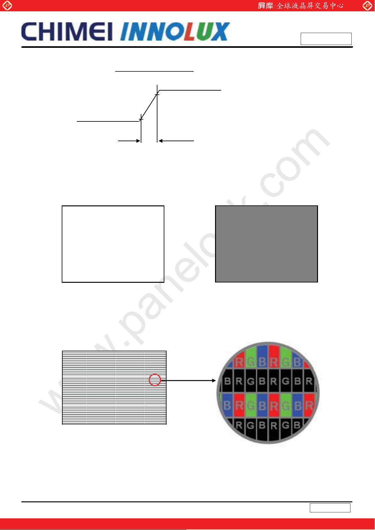
Pixel Arrangement RGB vertical stripe -
Display Colors 16.7M color
Display Operation Mode Transmissive mode / Normally black -
Surface Treatment Anti-Glare coating (Haze 11%),Hard coating (3H) -
(1)
1.5 MECHANICAL SPECIFICATIONS
Item Min. Typ. Max. Unit Note
Horizontal(H) 740.4 741.4 742.4 mm (1)
Module Size
Note (1) lease refer to the attached drawings for more information of front and back outline dimensions.
Note (2) Module Depth does not include connectors.
Vertical(V) 434.8 435.8 436.8 mm (1)
Depth(D) 25 26 27 mm To Cover
Depth(D) 14.2 15.2 16.2 mm To Rear
Weight -- (-) -- g
5
One step solution for LCD / PDP / OLED panel application: Datasheet, inventory and accessory!
Version 1.0
www.panelook.com
Page 6
Global LCD Panel Exchange Center
2. ABSOLUTE MAXIMUM RATINGS
2.1 ABSOLUTE RATINGS OF ENVIRONMENT
Item Symbol
Storage Temperature TST -20 +60 ºC (1)
Operating Ambient Temperature TOP 0 50 ºC (1), (2)
www.panelook.com
Min. Max.
Value
Issued Date: 13. Apr, 2010
Model No.: V315B5-LE1
Preliminary
Unit Note
Shock (Non-Operating) S
Vibration (Non-Operating) V
Note (1) Temperature and relative humidity range is shown in the figure below.
(a) 90 %RH Max. (Ta 40 ºC).Љ
(b) Wet-bulb temperature should be 39 ºC Max. (Ta > 40 ºC).
(c) No condensation.
Note (2) The maximum operating temperature is based on the test condition that the surface temperature of
display area is less than or equal to 65 ºC with LCD module alone in a temperature controlled chamber.
Thermal management should be considered in final product design to prevent the surface temperature
of display area from being over 65 ºC. The range of operating temperature may degrade in case of
improper thermal management in final product design.
Note (3) 11 ms, half sine wave, 1 time for ± X, ± Y, ± Z.
Note (4) 10 ~ 200 Hz, 30 min, 1 time each X, Y, Z.
Note (5) At testing Vibration and Shock, the fixture in holding the module has to be hard and rigid enough so that
the module would not be twisted or bent by the fixture.
- 50 G (3), (5)
NOP
- 1.0 G (4), (5)
NOP
Relative Humidity (%RH)
100
90
80
60
40
20
10
2.2 ELECTRICAL ABSOLUTE RATINGS
2.2.1 TFT LCD MODULE
Operating Range
Storage Range
8060-20 40 0 20 -40
Temperature (ºC)
6
One step solution for LCD / PDP / OLED panel application: Datasheet, inventory and accessory!
Version 1.0
www.panelook.com
Page 7
Global LCD Panel Exchange Center
www.panelook.com
Issued Date: 13. Apr, 2010
Model No.: V315B5-LE1
Preliminary
2.2 Package storage
When storing modules as spares for a long time, the following precaution is necessary.
(a) Do not leave the module in high temperature, and high humidity for a long time. It is highly recommended to
store the module with temperature from 0 to 35ഒat normal humidity without condensation.
(b) The module shall be stored in dark place. Do not store the TFT-LCD module in direct sunlight or
fluorescent light.
2.3 ELECTRICAL ABSOLUTE RATINGS
2.3.1 TFT LCD MODULE
Item Symbol
Power Supply Voltage Vcc -0.3 13.5 V
Input Signal Voltage VIN -0.3 3.6 V
Min. Max.
Value
Unit Note
(1)
2.3.2 BACKLIGHT CONVERTER UNIT
Item Symbol
Light Bar Voltage VW Ta = 25 к - - 60 V
Converter Input Voltage VBL - 0 - 30 V
Control Signal Level - - -0.3 - 7 V
Note (1) Permanent damage to the device may occur if maximum values are exceeded. Function operation
should be restricted to the conditions described under Normal Operating Conditions.
Te st
Condition
Min. Type Max. Unit Note
7
One step solution for LCD / PDP / OLED panel application: Datasheet, inventory and accessory!
Version 1.0
www.panelook.com
Page 8
Global LCD Panel Exchange Center
www.panelook.com
Issued Date: 13. Apr, 2010
Model No.: V315B5-LE1
Preliminary
3. ELECTRICAL CHARACTERISTICS
3.1 TFT LCD MODULE Ta = 25 ± 2 ºC
Value
Parameter Symbol
Min. Typ. Max.
Power Supply Voltage VCC 10.8 12 13.2 V (1)
Unit Note
Rush Current I
White Pattern
Power Supply Current
Horizontal Stripe
Black Pattern
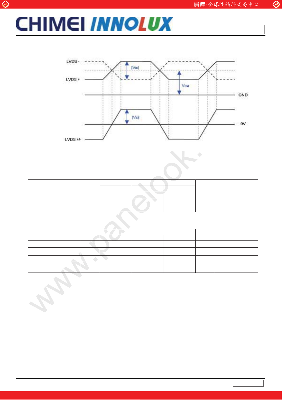
Differential Input High
Threshold Voltage
Differential Input Low
Threshold Voltage
LVDS
interface
Common Input Voltage VCM 1.0 1.2 1.4 V
Differential input
voltage(single-end)
Terminating Resistor R
CMOS
interface
Input High Threshold Voltage VIH 2.7
Input Low Threshold Voltage V
- - 4 A (2)
RUSH
Ё Ё
Ё Ё
Ё Ё
V
V
|V
LVT H
LVT L
ID
T
IL
+100
Ё Ё
| 200
Ё
0
Note (1) The module should be always operated within above ranges.
0.56
Ё
A
0.66 0.8 A
0.47
Ё Ё
Ё
A
mV
-100 mV
Ё
100
Ё
Ё
600 mV
Ё
ohm
3.3 V
0.7 V
(3)
(4)
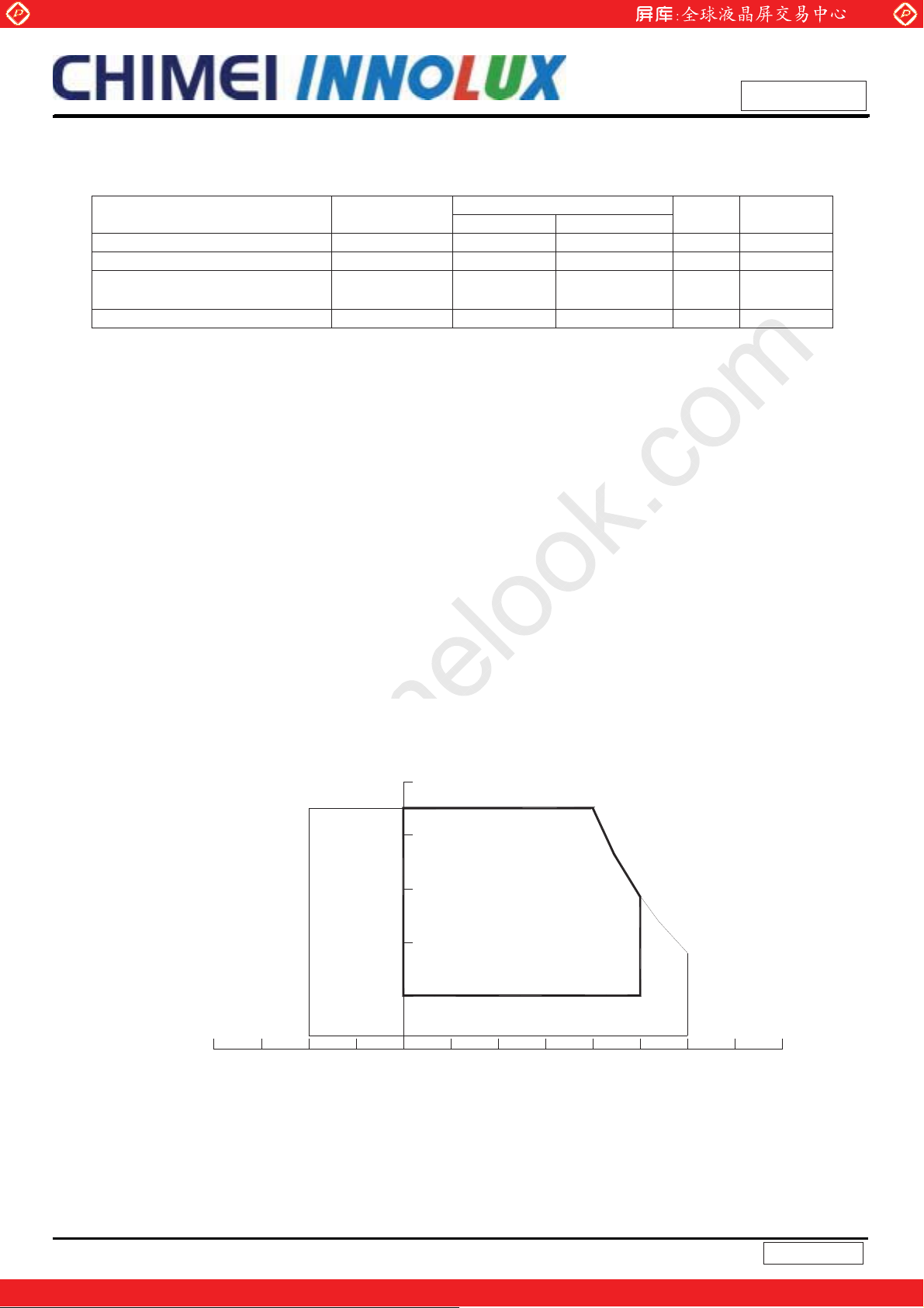
Note (2) Measurement Conditions:
+12.0V
(Low to High)
(Control Signal)
SW
R1
200K
Q1 AO4409
FUSE
VR1
47K
R2
1K
Q2
2N7002
C1
10uF
C3
1uF
Vcc
(LCD Module Input)
8
Version 1.0
One step solution for LCD / PDP / OLED panel application: Datasheet, inventory and accessory!
www.panelook.com
Page 9
Global LCD Panel Exchange Center
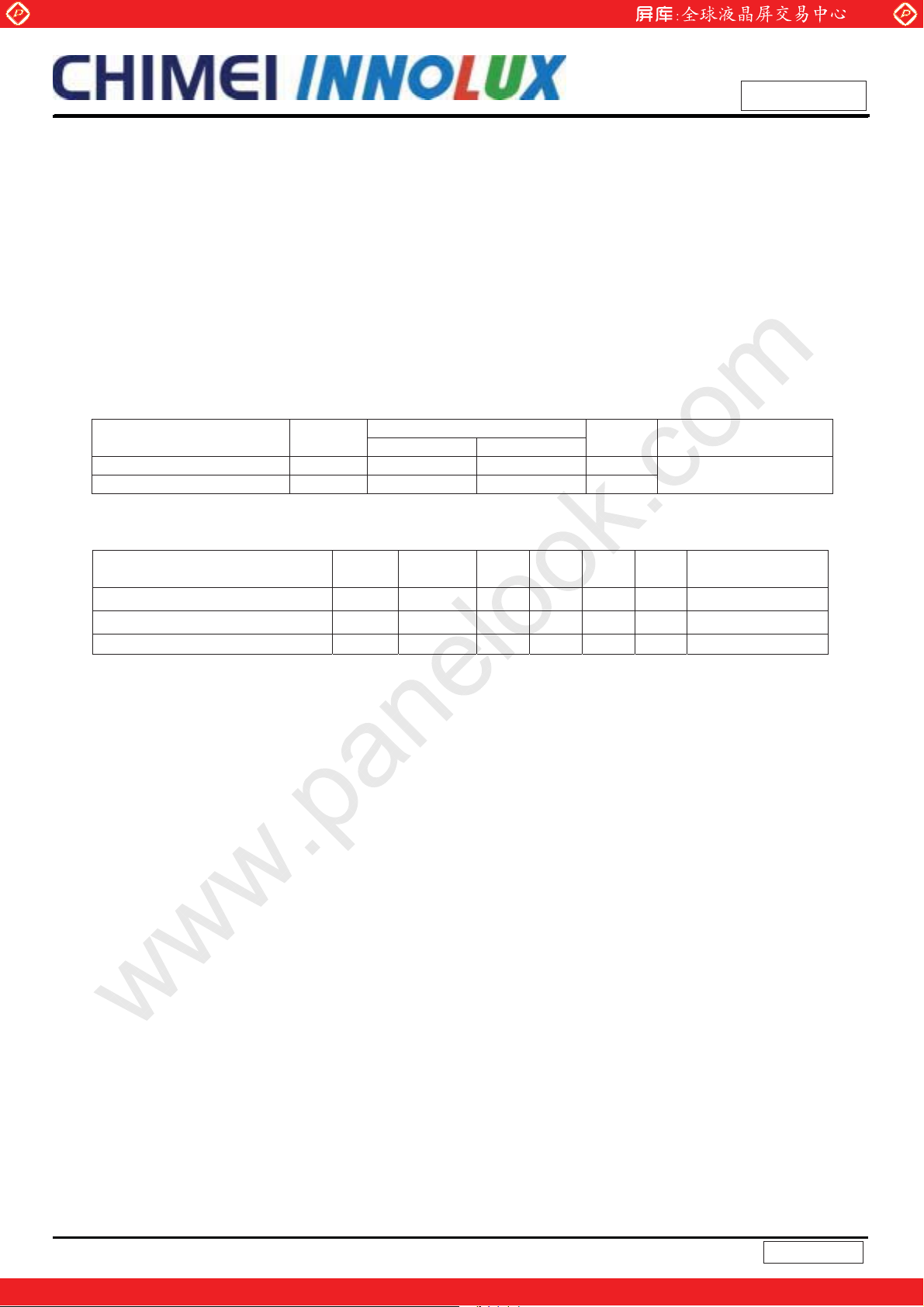
Vcc rising time is 470us
0.1Vcc
GND
www.panelook.com
Issued Date: 13. Apr, 2010
Model No.: V315B5-LE1
Preliminary
+12V
0.9Vcc
470us
Note (3) The specified power supply current is under the conditions at Vcc = 12 V, Ta = 25 ± 2 ºC, f
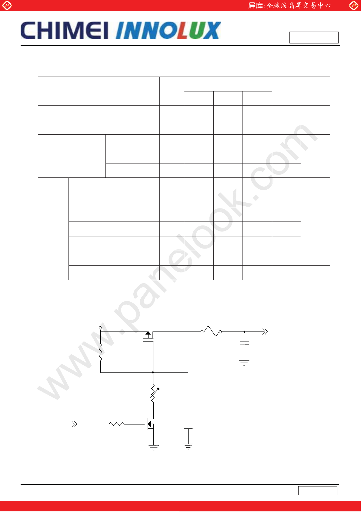
whereas a power dissipation check pattern below is displayed.
a. White Pattern
Active Area
c. Horizontal Pattern
b. Black Pattern
Active Area
= 60 Hz,
v
9
One step solution for LCD / PDP / OLED panel application: Datasheet, inventory and accessory!
Version 1.0
www.panelook.com
Page 10
Global LCD Panel Exchange Center
Note (4) The LVDS input characteristics are as follows:
www.panelook.com
Issued Date: 13. Apr, 2010
Model No.: V315B5-LE1
Preliminary
3.2 BACKLIGHT UNIT
3.2.1 LED LIGHT BARCHARACTERISTICS (
Parameter Symbol
Light Bar Voltage VW
Forward Voltage Vf
LED Current IL
Min. Typ. Max.
- - 51.0
- 3.1 3.4
75.2 80 84.8
Ta = 25 ± 2 ºC)
Value
Unit Note
V IL =80mA
V IL =80mA
mA
3.2.2 CONVERTER CHARACTERISTICS (Ta = 25 ± 2 ºC)
Parameter Symbol
Power Consumption PBL - 41.3 45.4 W
Converter Input Voltage VBL
Converter Input Current IBL - 1.72 1.89 A
Dimming Frequency FB 150 160 170 Hz
Minimum Duty Ratio D
Note (1) 5% minimum duty ratio is only valid for electrical operation.
5 10 -
MIN
Min. Typ. Max.
22.8 24 25.2
Value
Unit Note
VDC
%
(1)
10
One step solution for LCD / PDP / OLED panel application: Datasheet, inventory and accessory!
Version 1.0
www.panelook.com
Page 11
Global LCD Panel Exchange Center
3.2.3 CONVERTER INTERFACE CHARACTERISTICS
www.panelook.com
Issued Date: 13. Apr, 2010
Model No.: V315B5-LE1
Preliminary
Parameter Symbol
ON
On/Off Control Voltage
OFF
Internal PWM Control
Voltage
External PWM Control
Voltage
Error Signal ERR
VBL Rising Time Tr1
VBL Falling Time Tf1
Control Signal Rising Time Tr
MAX
MIN
HI
LO
VBLON
VIPWM
VEPWM
0
0
Value
Ё
Ё
0
Ё
Ё
Ё Ё
Ё Ё
5.0 V
0.8 V
Ё
5.0 V Duty on
0.8 V Duty off
100 ms
Te st
Condition
Ё
Ё
Ё
Ё Ё
Ё
Ё
Ё Ё Ё Ё Ё
Ё
Ё
Ё Ё Ё
Min. Typ. Max.
2.0
3.0 3.15 3.3
2.0
30
30
Unit Note
V maximum duty ratio
V minimum duty ratio
Abnormal: Open
collector
Normal: GND
(4)
ms
10%-90%V
ms
BL
Control Signal Falling Time Tf
PWM Signal Rising Time TPWMR
PWM Signal Falling Time TPWMF
Input Impedance Rin
PWM Delay Time TPWM
Ton
BLON Delay Time
T
on1
BLON Off Time Toff
Note (1) The Dimming signal should be valid before backlight turns on by BLON signal. It is inhibited to
change the internal/external PWM signal during backlight turn on period.
Note (2) The power sequence and control signal timing are shown in the following figure. For a certain
reason, the converter has a possibility to be damaged with wrong power sequence and control
signal timing.
Note (3) While system is turned ON or OFF, the power sequences must follow as below descriptions:
Ё Ё Ё
Ё Ё Ё
Ё Ё Ё
Ё
Ё
Ё
Ё
Ё
1
100
300
300
300
Ё Ё
Ё Ё
Ё Ё
Ё Ё
Ё Ё
100 ms
50 us
50 us
M
ms
ms
ms
ms
Turn ON sequence: VBL PWM signal BLON
Turn OFF sequence: BLOFF PWM signal VBL
Note (4) When converter protective function is triggered, ERR will output open collector status.
11
One step solution for LCD / PDP / OLED panel application: Datasheet, inventory and accessory!
Version 1.0
www.panelook.com
Page 12

Global LCD Panel Exchange Center
www.panelook.com
Issued Date: 13. Apr, 2010
Model No.: V315B5-LE1
Preliminary
V
VBLON
V
EPWM
V
IPWM
9
Toff
%/
Tf1
9
%/
Tr1
BL
0
9
0
%/
2.0V
0.8V
9%/
Ton
Ton1
Backlight on duration
Tr
Tf
Ext. Dimming Function
PWMR
T
2.0V
0
0.8V
T
PWM
T
PWMF
Floating
3.15V
0
Floating
Int. Dimming Function
V
W
External
PWM
Period
External
PWM Duty
100%
Minimun
Duty
12
One step solution for LCD / PDP / OLED panel application: Datasheet, inventory and accessory!
Version 1.0
www.panelook.com
Page 13

Global LCD Panel Exchange Center
q
)
www.panelook.com
Issued Date: 13. Apr, 2010
Model No.: V315B5-LE1
Preliminary
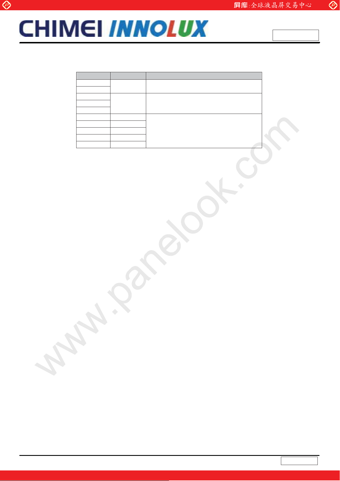
4. BLOCK DIAGRAM OF INTERFACE
4.1 TFT LCD MODULE
RX0(+/-)
RX1(+/-)
RX2(+/-)
RX3(+/-)
RXCLK(+/-)
ODSEL
Vcc
GND
VBL
GND
ERR
BLON
I_PWM
E_PWM
(STARCONN 093G30-B0001A
or P-TWO 187053-30091 or
E
uivalent
DC/DC CONVERTER &
REFERENCE VOLTAGE
CONVERTER
CONNECTOR
CN1: Cvilux CI0114M1HR0-LA
or Equivalent
FRAME BUFFER
CONTROLLER
SCAN DRIVER IC
TFT LCD PANEL
(1366x3x768)
TIMING
DATA DRIVER IC
CN2,3 : 51281-1094 (Molex) or Equivalent
LED
BACKLIGHT
UNIT
One step solution for LCD / PDP / OLED panel application: Datasheet, inventory and accessory!
13
Version 1.0
www.panelook.com
Page 14

Global LCD Panel Exchange Center
www.panelook.com
5. INTERFACE PIN CONNECTION
5.1 TFT LCD MODULE
CNF1 Connector Pin Assignment
Pin No. Symbol Description Note
1 VCC Power supply: +12V
2 VCC Power supply: +12V
3 VCC Power supply: +12V
4 VCC Power supply: +12V
5 GND Ground
6 GND Ground
7 GND Ground
8 NC No connection (4)
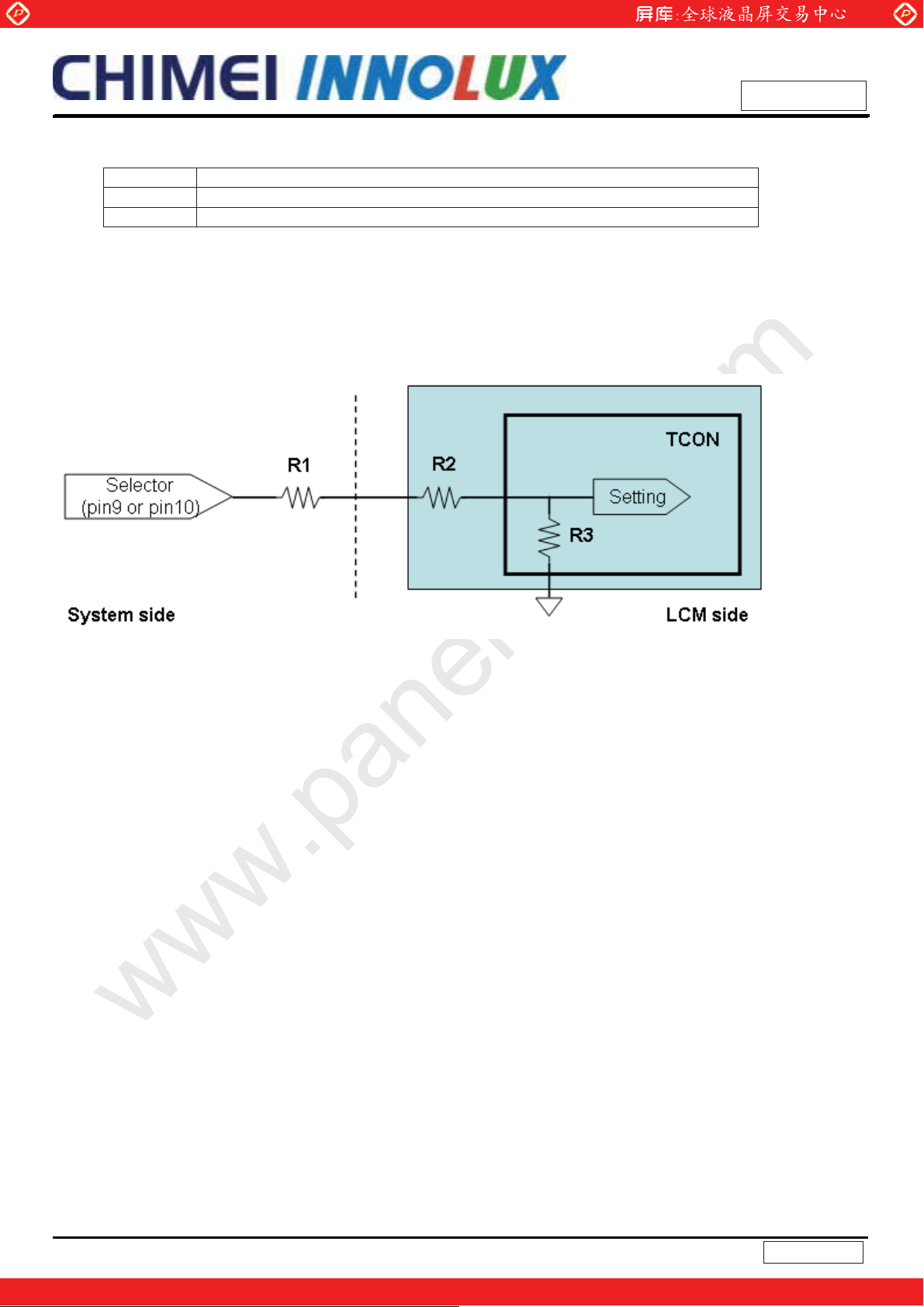
9 SELLVDS Select LVDS data format (2),(5)
10 ODSEL Overdrive Lookup Table Selection (3),(5)
11 GND Ground
12 RX0- Negative transmission data of pixel 0
13 RX0+ Positive transmission data of pixel 0
14 GND Ground
15 RX1- Negative transmission data of pixel 1
16 RX1+ Positive transmission data of pixel 1
17 GND Ground
18 RX2- Negative transmission data of pixel 2
19 RX2+ Positive transmission data of pixel 2
20 GND Ground
21 RXCLK- Negative of clock
22 RXCLK+ Positive of clock
23 GND Ground
24 RX3- Negative transmission data of pixel 3
25 RX3+ Positive transmission data of pixel 3
26 GND Ground
27 NC No connection (4)
28 NC No connection (4)
29 NC No connection (4)
30 GND Ground
Note (1) Connector Part No.: STARCONN 093G30-B0001A or P-TWO 187053-30091 or Equivalent
Issued Date: 13. Apr, 2010
Model No.: V315B5-LE1
Preliminary
LVDS connector pin order defined as follows
Note (2) Low = Open or connect to GND: VESA Format, High = Connect to +3.3V: JEIDA Format.
Please refer to 5.5 LVDS INTERFACE
Note (3) Overdrive lookup table selection. The Overdrive lookup table should be selected in accordance to the
frame rate to optimize image quality.
14
One step solution for LCD / PDP / OLED panel application: Datasheet, inventory and accessory!
Version 1.0
www.panelook.com
Page 15
Global LCD Panel Exchange Center
Low = Open or connect to GND, High = Connect to +3.3V
ODSEL Note
L or Open Lookup table was optimized for 60 Hz frame rate.
H Lookup table was optimized for 50 Hz frame rate.
Note (4) Reserved for internal use. Left it open.
Note (5) LVDS signal pin connected to the LCM side has the following diagram.
R1 in the system side should be less than 1K Ohm. (R1 < 1K Ohm)
www.panelook.com
Issued Date: 13. Apr, 2010
Model No.: V315B5-LE1
Preliminary
15
One step solution for LCD / PDP / OLED panel application: Datasheet, inventory and accessory!
Version 1.0
www.panelook.com
Page 16
Global LCD Panel Exchange Center
5.2 BACKLIGHT UNIT
The pin configuration for the housing and the leader wire is shown in the table below.
www.panelook.com
Issued Date: 13. Apr, 2010
Model No.: V315B5-LE1
Preliminary
CN2: Molex 51281-1094
or Equivalent
Pin Symbol Feature
1
2
3
4
5
6 N1
7 N2
8 N3
9 N4
10 N5
VLED+ Positive of LED String
NC NC
5.3 CONVERTER UNIT
CN1(Header): Cvilux CI0114M1HR0-LA or Equivalent
Pin Symbol Feature
1
Negative of LED String
2
3
4
5
6
7
8
9
10
11 ERR
12 BLON BL ON/OFF
13 I_PWM
14 E_PWM
VBL +24V
GND GND
Normal (GND)
Abnormal (Open
collector)
Internal PWM
Control
External PWM
Control
Note (1) Pin 13: Internal PWM Control (Use Pin 13): Pin 14 must open.
Note (2) Pin 14: External PWM Control (Use Pin 14): Pin 13 must open.
Note (3) Pin 13(I_PWM) and Pin 14(E_PWM) can’t open in same period.
16
One step solution for LCD / PDP / OLED panel application: Datasheet, inventory and accessory!
Version 1.0
www.panelook.com
Page 17
Global LCD Panel Exchange Center
CN2,3: 51281-1094(Molex) or Equivalent
Pin Symbol Feature
1
2
3
4
5
6 N1
7 N2
8 N3
9 N4
10 N5
www.panelook.com
Issued Date: 13. Apr, 2010
Model No.: V315B5-LE1
Preliminary
VLED+ Positive of LED String
NC NC
Negative of LED String
17
One step solution for LCD / PDP / OLED panel application: Datasheet, inventory and accessory!
Version 1.0
www.panelook.com
Page 18
Global LCD Panel Exchange Center
G0-G
0
p
5.4 BLOCK DIAGRAM OF INTERFACE
www.panelook.com
Issued Date: 13. Apr, 2010
Model No.: V315B5-LE1
Preliminary
CNF1
Rx0+
Rx
R0-R7
TxIN
7
B0-B7
DE
-
Rx1+
Rx1-
Rx2+
Rx2-
Rx3+
Rx3-
Host
Graphics
Controller
PLL
CLK+
CLK-
LVDS Transmitter
THC63LVDM83A
(LVDF83A)
51Ө
100pF
51Ө
51Ө
F
100
51Ө
51Ө
100pF
51Ө
51Ө
100pF
51Ө
51Ө
100pF
51Ө
PLL
LVDS Receiver
THC63LVDF84A
Rx
R0-R7
G0-G7
B0-B7
DE
DCLK
Timing
Controller
R0~R7 : Pixel R Data
G0~G7 : Pixel G Data
B0~B7 : Pixel B Data
DE : Data Enable Signal
DCLK : Data clock signal
Note (1) The system must have the transmitter to drive the module.
Note (2) LVDS cable impedance shall be 50 ohms per signal line or about 100 ohms per twist-pair line when it is
used differentially.
18
One step solution for LCD / PDP / OLED panel application: Datasheet, inventory and accessory!
Version 1.0
www.panelook.com
Page 19

Global LCD Panel Exchange Center
5.5 LVDS INTERFACE
VESA LVDS formatΚ(SELLVDS pin=L or open)
www.panelook.com
Issued Date: 13. Apr, 2010
Model No.: V315B5-LE1
Preliminary
JEDIA LVDS formatΚ(SELLVDS pin=H)
R0~R7: Pixel R Data (7; MSB, 0; LSB)
G0~G7: Pixel G Data (7; MSB, 0; LSB)
B0~B7: Pixel B Data (7; MSB, 0; LSB)
DE : Data enable signal
Notes(1) RSVD(reserved)pins on the transmitter shall be “H” or( “L” or OPEN)
19
One step solution for LCD / PDP / OLED panel application: Datasheet, inventory and accessory!
Version 1.0
www.panelook.com
Page 20

Global LCD Panel Exchange Center
www.panelook.com
Issued Date: 13. Apr, 2010
Model No.: V315B5-LE1
Preliminary
5.6 COLOR DATA INPUT ASSIGNMENT
The brightness of each primary color (red, green and blue) is based on the 8-bit gray scale data input for the color.
The higher the binary input, the brighter the color. The table below provides the assignment of the color versus data
input.
Data Signal
Color
R7 R6 R5 R4 R3 R2 R1 R0 G7 G6 G5 G4 G3 G2 G1 G0 B7 B6 B5 B4 B3 B2 B1 B0
Black
Red
Green
Basic
Colors
Gray
Scale
Of
Red
Gray
Scale
Of
Green
Gray
Scale
Of
Blue
Blue
Cyan
Magenta
Yellow
White
Red(0) / Dark
Red(1)
Red(2)
:
:
Red(253)
Red(254)
Red(255)
Green(0) / Dark
Green(1)
Green(2)
:
:
Green(253)
Green(254)
Green(255)
Blue(0) / Dark
Blue(1)
Blue(2)
:
:
Blue(253)
Blue(254)
Blue(255)
Note (1) 0: Low Level Voltage, 1: High Level Voltage
0
1
0
0
0
1
1
1
0
0
0
1
1
1
0
0
0
0
0
0
0
0
0
0
0
0
0
1
0
0
0
1
1
1
0
0
0
:
:
:
:
1
1
1
0
0
0
:
:
:
:
0
0
0
0
0
0
:
:
:
:
0
0
0
Red Green Blue
0
0
0
0
0
0
0
0
0
0
0
0
0
0
0
0
0
0
0
0
0
1
1
1
1
1
1
0
0
0
0
0
0
0
0
0
0
0
0
0
0
0
0
0
0
0
0
0
1
1
1
1
1
1
1
1
0
0
0
0
0
0
0
0
0
0
0
0
0
0
0
0
0
0
0
0
0
1
1
1
1
1
1
1
0
0
0
0
0
0
1
1
1
1
1
1
1
1
1
1
1
1
1
1
1
1
1
1
1
1
1
0
0
0
0
0
0
0
0
1
1
1
1
1
1
1
1
1
1
1
1
1
1
1
1
1
1
1
1
1
0
0
0
0
0
0
0
1
1
1
1
1
1
1
1
1
1
1
1
1
1
1
1
1
1
1
1
1
0
0
0
0
0
0
0
0
0
0
0
0
0
0
0
0
0
0
0
0
0
0
0
0
0
0
1
0
0
0
0
0
0
0
0
0
0
0
0
0
0
0
0
0
0
0
1
0
0
0
0
0
0
0
0
0
0
0
0
0
0
0
0
:
:
:
:
:
:
:
:
:
:
:
:
:
:
:
:
:
:
:
:
:
:
:
:
:
:
:
:
:
:
:
:
:
:
:
:
:
:
:
:
:
:
1
1
1
1
0
1
0
0
0
0
0
0
0
0
0
0
0
0
0
0
0
1
1
1
1
1
0
0
0
0
0
0
0
0
0
0
0
0
0
0
0
0
1
1
1
1
1
1
0
0
0
0
0
0
0
0
0
0
0
0
0
0
0
0
0
0
0
0
0
0
0
0
0
0
0
0
0
0
0
0
0
0
0
0
0
0
0
0
0
0
0
0
0
0
0
0
0
1
0
0
0
0
0
0
0
0
0
0
0
0
0
0
0
0
0
0
0
1
0
0
0
0
0
0
0
0
:
:
:
:
:
:
:
:
:
:
:
:
:
:
:
:
:
:
:
:
:
:
:
:
:
:
:
:
:
:
:
:
:
:
:
:
:
:
:
:
:
:
0
0
0
0
0
0
1
1
1
1
1
1
0
1
0
0
0
0
0
0
0
0
0
0
0
0
0
1
1
1
1
1
1
1
0
0
0
0
0
0
0
0
0
0
0
0
0
0
1
1
1
1
1
1
1
1
0
0
0
0
0
0
0
0
0
0
0
0
0
0
0
0
0
0
0
0
0
0
0
0
0
0
0
0
0
0
0
0
0
0
0
0
0
0
0
0
0
0
0
0
0
0
0
0
0
0
0
0
0
0
0
0
0
0
0
0
0
0
0
0
0
0
0
0
0
1
:
:
:
:
:
:
:
:
:
:
:
:
:
:
:
:
:
:
:
:
:
:
:
:
:
:
:
:
:
:
:
:
:
:
:
:
:
:
:
:
:
:
0
0
0
0
0
0
0
0
0
0
0
0
0
0
1
1
1
1
1
1
0
0
0
0
0
0
0
0
0
0
0
0
0
0
0
1
1
1
1
1
1
1
0
0
0
0
0
0
0
0
0
0
0
0
0
0
1
1
1
1
1
1
1
0
0
0
1
1
1
0
1
0
0
0
:
:
0
0
0
0
0
0
:
:
0
0
0
0
1
0
:
:
1
0
1
20
One step solution for LCD / PDP / OLED panel application: Datasheet, inventory and accessory!
Version 1.0
www.panelook.com
Page 21

Global LCD Panel Exchange Center
6. INTERFACE TIMING
6.1 INPUT SIGNAL TIMING SPECIFICATIONS
The input signal timing specifications are shown as the following table and timing diagram.
Signal Item Symbol Min. Typ. Max. Unit Note
Frequency
(=1/TC)
Input cycle to
LVDS
Receiver
Clock
cycle jitter
Spread spectrum
modulation range
F
Spread spectrum
modulation
frequency
LVDS
Setup Time
Receiver
Data
Hold Time
www.panelook.com
Issued Date: 13. Apr, 2010
F
clkin
T
rcl
clkin_mod
F
200 KHz
SSM
Tlvsu 600
Tlvhd 600
60 76 82 MHz
Ё Ё
F
-2%
clkin
Ё
200 ps (3)
F
+2% MHz
clkin
Ё Ё
Ё Ё
Model No.: V315B5-LE1
Preliminary
(4)
ps
(5)
ps
Vertical
Active
Frame Rate
Tot al
Fr5 47 50 53 Hz
Fr6 57 60 63 Hz
Tv 778 806 888 Th
(6)
Tv=Tvd+Tvb
Display
Term
Display
Blank
Horizontal
Active
Display
Term
Note (1) Please make sure the range of pixel clock has follow the below equationΚ
Note (2) This module is operated in DE only mode and please follow the input signal timing diagram belowΚ
Tot al
Display
Blank
Fclkin(max) Њ Fr6 Ѽ Tv Ѽ Th
Fr5 Ѽ Tv Ѽ Th Њ Fclkin(min)
Tvd 768 768 768 Th
Tvb 10 38 120 Th
Th 1442 1560 1936 Tc
Thd 1366 1366 1366 Tc
Thb 76 194 570 Tc
Ё
Ё
Th=Thd+Thb
Ё
Ё
21
One step solution for LCD / PDP / OLED panel application: Datasheet, inventory and accessory!
Version 1.0
www.panelook.com
Page 22

Global LCD Panel Exchange Center
www.panelook.com
Issued Date: 13. Apr, 2010
Model No.: V315B5-LE1
Preliminary
INPUT SIGNAL TIMING DIAGRAM
DE
Th
DCLK
Tc
DE
DATA
Tvd
Thb
Tv
Tvb
Thd
Valid Display Data (1366 clocks)
Note (3) The input clock cycle-to-cycle jitter is defined as below figures. Trcl = I T1 – TI
22
One step solution for LCD / PDP / OLED panel application: Datasheet, inventory and accessory!
Version 1.0
www.panelook.com
Page 23

Global LCD Panel Exchange Center
Note (4) The SSCG (Spread spectrum clock generator) is defined as below figures
www.panelook.com
Issued Date: 13. Apr, 2010
Model No.: V315B5-LE1
Preliminary
Note (5) The LVDS timing diagram and setup/hold time is defined and showing as the following figures.
RXCLK+/-
RXn+/-
LVDS RECEIVER INTERFACE TIMING DIAGRAM
Tc
Tlvsu
Tlvhd
1T
14
Note (6) : (ODSEL) = H/L or open for 50/60Hz frame rate. Please refer to 5.1 for detail information
One step solution for LCD / PDP / OLED panel application: Datasheet, inventory and accessory!
3T
14
5T
14
7T
14
23
9T
14
11T
14
13T
14
Version 1.0
www.panelook.com
Page 24

Global LCD Panel Exchange Center
Љ
Љ
Љ
Љ
Љ
P
Љ
Љ
Љ
6.2 POWER ON/OFF SEQUENCE
To prevent a latch-up or DC operation of LCD module, the power on/off sequence should be as the diagram
below.
www.panelook.com
Issued Date: 13. Apr, 2010
Model No.: V315B5-LE1
Preliminary
0.9V
CC
0.9V
CC
50ms
50ms
T
0V
4
0.5ЉT1Љ10ms
0
0
500ms
2
T
3
T
0.1V
CC
T
3 T1
T
2
0.1V
cc
T4
LVDS Signals
0V
Power On
VALI D
0ЉT7ЉT2
0
T
8
T3
T7
8
T
Option Signals
(SELLVDS, ODSEL)
Backlight (Recommended)
500ms
100msЉT6
T
5
50%
T
5
50%
T
6
Power ON/OFF Sequence
Note (1) The supply voltage of the external system for the module input should follow the definition of Vcc.
Note (2) Apply the LED voltage within the LCD operation range. When the backlight turns on before the LCD
operation or the LCD turns off before the backlight turns off, the display may momentarily become
abnormal screen.
Note (3) In case of Vcc is in off level, please keep the level of input signals on the low or high impedance. If
T2<0,that maybe cause electrical overstress failure.
Note (4) T4 should be measured after the module has been fully discharged between power off and on period.
Note (5) Interface signal shall not be kept at high impedance when the power is on.
24
Version 1.0
One step solution for LCD / PDP / OLED panel application: Datasheet, inventory and accessory!
www.panelook.com
Page 25

Global LCD Panel Exchange Center
y
(
)
(
)
)
(
)
(
)
)
(
)
(4)
)
(
y (
(
y (
(
y (
(
y
(
(80)
(88)
(80)
(88)
(80)
(88)
(80)
(88)
7. OPTICAL CHARACTERISTICS
7.1 TEST CONDITIONS
Item Symbol Value Unit
Ambient Temperature Ta
Ambient Humidity Ha
Supply Voltage VCC 12V V
Input Signal According to typical value in "3. ELECTRICAL CHARACTERISTICS"
LED Current IL
7.2 OPTICAL SPECIFICATIONS
The relative measurement methods of optical characteristics are shown in 7.2. The following items should be
measured under the test conditions described in 7.1 and stable environment shown in Note (6).
Item S
Contrast Ratio CR
www.panelook.com
Issued Date: 13. Apr, 2010
Model No.: V315B5-LE1
Preliminary
o
25r2
50r10
80r4.8
mbol Condition Min. Typ. Max. Unit Note
2500
3000
- (2
C
%RH
mA
Response Time
Center Luminance of White L
White Variation
Cross Talk CT
Red
Green
Color
Chromaticity
Viewing
Angle
Blue
White
Color Gamut CG
Horizontal
Vertical
Gray to gray
average
C
GW
Rx
R
Gx
G
Bx
B
Wx
W
T
+
T
-
T
+
-
T
=0q, TY =0q
T
x
Viewing Normal
Angle
CRt20
- 8.5 14 ms (3)
320
Typ.
-0.03
400
0.627) -
0.323) -
0.312) -
0.623) -
0.154) -
0.049) -
0.280)
0.290)
72
(4
1.3) - (7
% (5
Typ.
+0.03
Target
% NTSC
Deg. (1)
(6)
25
One step solution for LCD / PDP / OLED panel application: Datasheet, inventory and accessory!
Version 1.0
www.panelook.com
Page 26
Global LCD Panel Exchange Center
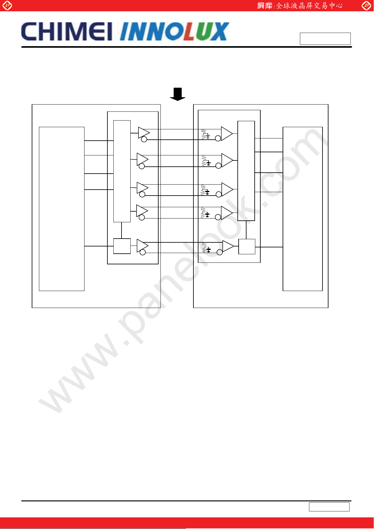
Note (1) Definition of Viewing Angle (Tx, Ty):
Viewing angles are measured by Autronic Conoscope Cono-80
www.panelook.com
Issued Date: 13. Apr, 2010
Model No.: V315B5-LE1
Preliminary
TX- = 90º
x-
6 o’clock
T
y- = 90º
y-
Note (2) Definition of Contrast Ratio (CR):
The contrast ratio can be calculated by the following expression.
Contrast Ratio (CR) = L255 / L0
L255: Luminance of gray level 255
Normal
Tx = Ty = 0º
Ty- Ty
Tx
Tx
12 o’clock direction
y+
T
y+ = 90º
x+
TX+ = 90º
L 0: Luminance of gray level 0
CR = CR (5), where CR (X) is corresponding to the Contrast Ratio of the point X at the figure in Note
(7)
Note (3) Definition of Gray-to-Gray Switching Time:
Optical
Response
100%
90%
10%
0%
Gray to gray
Switching time
The driving signal means the signal of luminance 0%, 20%, 40%, 60%, 80%, 100%.
Gray to gray average time means the average switching time of luminance 0%, 20%,
40%, 60%, 80%, 100% to each other.
Gray to gray
Switching time
Time
26
One step solution for LCD / PDP / OLED panel application: Datasheet, inventory and accessory!
Version 1.0
www.panelook.com
Page 27
Global LCD Panel Exchange Center
A
A
Note (4) Definition of Luminance of White (LC):
www.panelook.com
Issued Date: 13. Apr, 2010
Model No.: V315B5-LE1
Preliminary
Measure the luminance of gray level 255 at center point.
LC = L (5), where L (x) is corresponding to the luminance of the point X at the figure in Note (7).
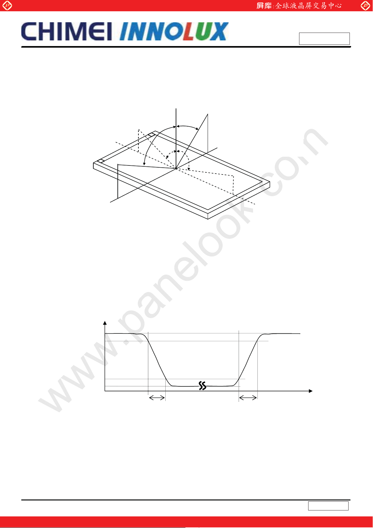
Note (5) Definition of Cross Talk (CT):
CT = | Y
– YA | / YA u 100 (%)
B
Where:
Y
= Luminance of measured location without gray level 0 pattern (cd/m2)
A
Y
= Luminance of measured location with gray level 0 pattern (cd/m2)
B
(0, 0)
ctive Area
Gray 0
Y
(D/8,W/2)
A, L
Gray 128
Y
(D/2,7W/8)
A, D
Y
A, U
Y
A, R
(D, W)
(D/2,W/8)
(7D/8,W/2)
(D/4,W/4)
Y
(D/8,W/2)
B, L
Y
(D/2,7W/8)
B, D
(0, 0)
ctive Area
Gray 255
Y
(D/2,W/8)
B, U
Y
(7D/8,W/2)
B, R
(3D/4,3W/4)
(D, W)
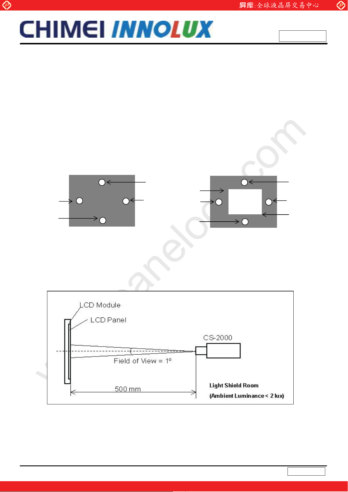
Note (6) Measurement Setup:
The LCD module should be stabilized at given temperature for 1 hour to avoid abrupt
temperature change during measuring. In order to stabilize the luminance, the measurement
should be executed after lighting backlight for 1 hour in a windless room.
27
One step solution for LCD / PDP / OLED panel application: Datasheet, inventory and accessory!
Version 1.0
www.panelook.com
Page 28

Global LCD Panel Exchange Center
Note (7) Definition of White Variation (GW):
Measure the luminance of gray level 255 at 5 points
GW = Maximum [L (1), L (2), L (3), L (4), L (5)] / Minimum [L (1), L (2), L (3), L (4), L (5)]
www.panelook.com
Issued Date: 13. Apr, 2010
Model No.: V315B5-LE1
Preliminary
Horizontal Line
Vertical Line
W
W/4
W/2
3W/4
D/4 D/2 3D/4
1 2
3 4
D
5
Active Area
X
: Test Point
X=1 to 5
28
One step solution for LCD / PDP / OLED panel application: Datasheet, inventory and accessory!
Version 1.0
www.panelook.com
Page 29
Global LCD Panel Exchange Center
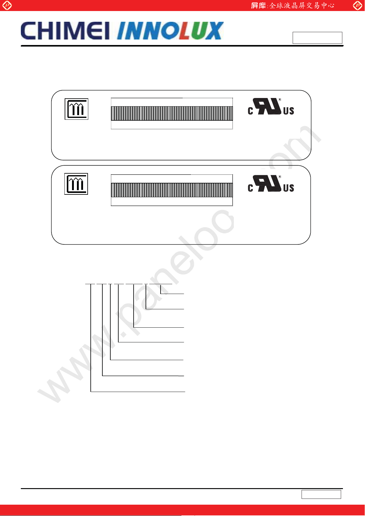
8. DEFINITION OF LABELS
8.1 CMO MODULE LABEL
The barcode nameplate is pasted on each module as illustration, and its definitions are as following explanation.
www.panelook.com
V315B5 -LE1 Rev. XX
Issued Date: 13. Apr, 2010
Model No.: V315B5-LE1
Preliminary
CHI MEI
OPTOELECTRONICS
X X X X X X X Y M D L N N N N
E207943
MADE IN TAIWAN
GEMN
V315B5 -LE1 Rev. XX
CHI MEI
OPTOELECTRONICS
X X X X X X X Y M D L N N N N
E207943
MADE IN TAIWAN
MADE IN CHINA
LEOO(or CAPG or CANO)
(a) Model Name: V315B5-LE1
(b) Revision: Rev. XX, for example: A0, A1… B1, B2… or C1, C2…etc.
(c) Serial ID: X X
X X X X X Y M D L N N N N
Serial No.
Product Line
RoHS
Serial ID includes the information as below:
(a) Manufactured Date: Year: 0~9, for 2010~2019
Month: 1~9, A~C, for Jan. ~ Dec.
Day: 1~9, A~Y, for 1
(b) Revision Code: Cover all the change
(c) Serial No.: Manufacturing sequence of product
(d) Product Line: 1 -> Line1, 2 -> Line 2, …etc.
Year, Month, Date
CMO Internal Use
CMO Internal Use
Revision
CMO Internal Use
st
to 31st, exclude I ,O, and U.
29
Version 1.0
One step solution for LCD / PDP / OLED panel application: Datasheet, inventory and accessory!
www.panelook.com
Page 30
Global LCD Panel Exchange Center
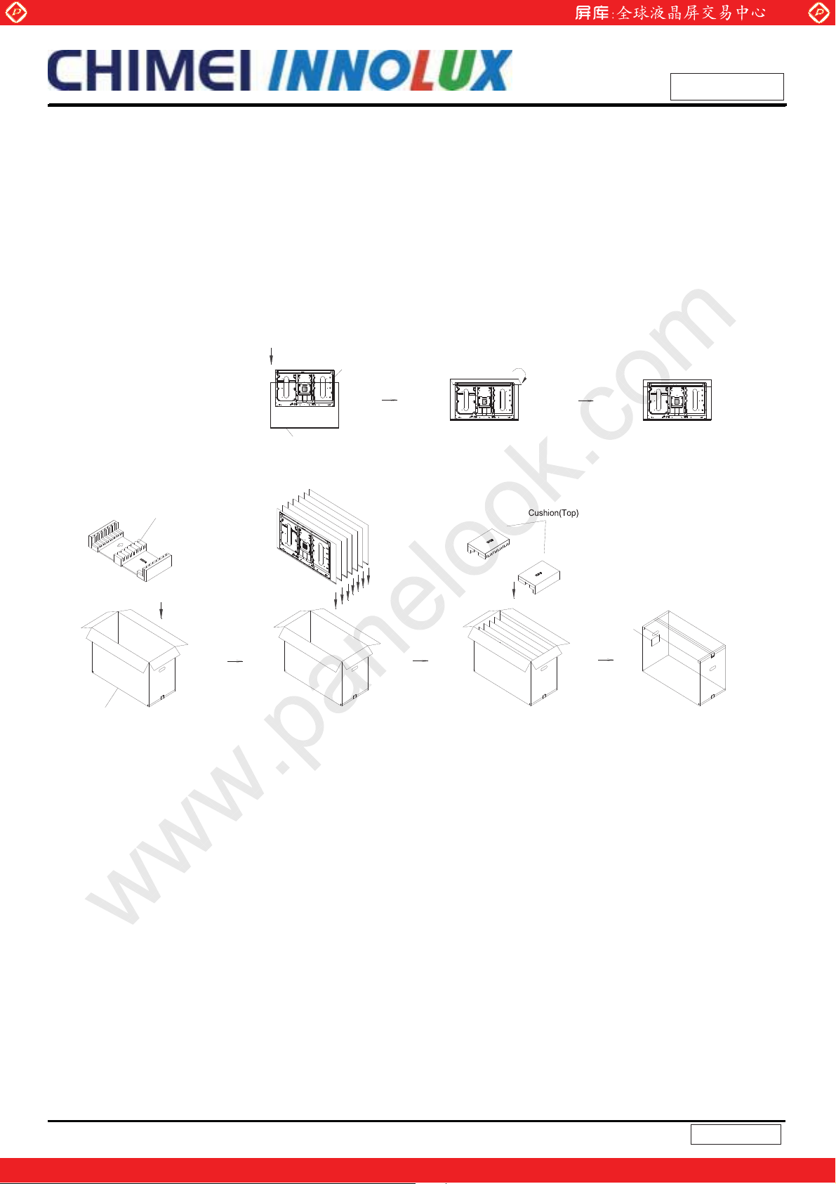
9. PACKAGING
9.1 PACKING SPECIFICATIONS
(1) 7 LCD TV modules / 1 Box
(2) Box dimensions : 826(L)x376(W)x540(H)mm
(3) Weight : approximately 50 Kg (7 modules per box)
9.2 PACKING METHOD
Figures 9-1 and 9-2 are the packing method
www.panelook.com
Issued Date: 13. Apr, 2010
Model No.: V315B5-LE1
Preliminary
LCD TV Module
Carton
Anti-static Bag
Cushion
Carton Label
Figure.9-1 packing method
30
One step solution for LCD / PDP / OLED panel application: Datasheet, inventory and accessory!
Version 1.0
www.panelook.com
Page 31
Global LCD Panel Exchange Center
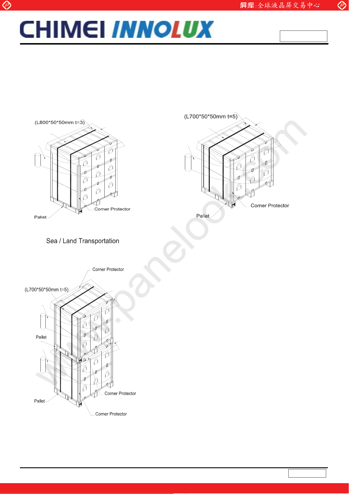
Sea / Land Transportation
(40ft Container)
Corner Protector
PE Sheet
PP Belt
www.panelook.com
Issued Date: 13. Apr, 2010
Model No.: V315B5-LE1
Preliminary
Air Transportation
Corner Protector
PE Sheet
PP Belt
Film
(L1150*W850*140mm )
(40ft HQ Container)
Corner Protector
Film
(L1350*50*50mm t=3)
(L700*50*50mm t=5)
PP Belt
PE Sheet
Film
(L1080*50*50mm t=5)
(L1150*W850*140mm)
PE Sheet
Film
(L700*50*50mm t=5)
(L1150*W850*140mm)
(L1055*50*50mm t=5)
Figure. 9-2 Packing method
31
One step solution for LCD / PDP / OLED panel application: Datasheet, inventory and accessory!
Version 1.0
www.panelook.com
Page 32

Global LCD Panel Exchange Center
www.panelook.com
Issued Date: 13. Apr, 2010
Model No.: V315B5-LE1
Preliminary
10. PRECAUTIONS
10.1 ASSEMBLY AND HANDLING PRECAUTIONS
(1) Do not apply rough force such as bending or twisting to the module during assembly.
(2) It is recommended to assemble or to install a module into the user’s system in clean working areas. The
dust and oil may cause electrical short or worsen the polarizer.
(3) Do not apply pressure or impulse to the module to prevent the damage of LCD panel and backlight.
(4) Always follow the correct power-on sequence when the LCD module is turned on. This can prevent the
damage and latch-up of the CMOS LSI chips.
(5) Do not plug in or pull out the I/F connector while the module is in operation.
(6) Do not disassemble the module.
(7) Use a soft dry cloth without chemicals for cleaning, because the surface of polarizer is very soft and
easily scratched.
(8) Moisture can easily penetrate into LCD module and may cause the damage during operation.
(9) High temperature or humidity may deteriorate the performance of LCD module. Please store LCD
modules in the specified storage conditions.
(10) When ambient temperature is lower than 10ºC, the display quality might be reduced. For example, the
response time will become slow, and the starting voltage of CCFL will be higher than that of room
temperature.
10.2 SAFETY PRECAUTIONS
(1) The startup voltage of a backlight is over 1000 Volts. It may cause an electrical shock while assembling
with the inverter. Do not disassemble the module or insert anything into the backlight unit.
(2) If the liquid crystal material leaks from the panel, it should be kept away from the eyes or mouth. In
case of contact with hands, skin or clothes, it has to be washed away thoroughly with soap.
(3) After the module’s end of life, it is not harmful in case of normal operation and storage.
10.3 STORAGE PRECAUTIONS
When storing modules as spares for a long time, the following precaution is necessary.
(1) Do not leave the module in high temperature, and high humidity for a long time.
It is highly recommended to store the module with temperature from 0 to 35кat normal humidity without
condensation.
(2) The module shall be stored in dark place. Do not store the TFT-LCD module in direct sunlight or fluorescent
light.
32
One step solution for LCD / PDP / OLED panel application: Datasheet, inventory and accessory!
Version 1.0
www.panelook.com
Page 33

Global LCD Panel Exchange Center
www.panelook.com
11. REGULATORY STANDARDS
11.1 SAFETY
The LCD module should be certified with safety regulations as follows:
Requirement Standard Remark
UL
cUL/CSA
CB
UL60950-1:2006 or Ed.2:2007
UL60065 Ed.7:2007
CAN/CSA C22.2 No.60950-1-03 or 60950-1-07
CAN/CSA C22.2 No.60065-03:2006 + A1:2006
IEC60950-1:2005 / EN60950-1:2006+ A11:2009
IEC60065:2001+ A1:2005 / EN60065:2002 + A1:2006 + A11:2008
Issued Date: 13. Apr, 2010
Model No.: V315B5-LE1
Preliminary
33
One step solution for LCD / PDP / OLED panel application: Datasheet, inventory and accessory!
Version 1.0
www.panelook.com
Page 34

Global LCD Panel Exchange Center
12. MECHANICAL CHARACTERISTIC
www.panelook.com
Issued Date: 13. Apr, 2010
Model No.: V315B5-LE1
Preliminary
34
One step solution for LCD / PDP / OLED panel application: Datasheet, inventory and accessory!
Version 1.0
www.panelook.com
Page 35

Global LCD Panel Exchange Center
www.panelook.com
Issued Date: 13. Apr, 2010
Model No.: V315B5-LE1
Preliminary
35
One step solution for LCD / PDP / OLED panel application: Datasheet, inventory and accessory!
Version 1.0
www.panelook.com
Page 36

Global LCD Panel Exchange Center
www.panelook.com
Issued Date: 13. Apr, 2010
Model No.: V315B5-LE1
Preliminary
36
One step solution for LCD / PDP / OLED panel application: Datasheet, inventory and accessory!
Version 1.0
www.panelook.com
 Loading...